

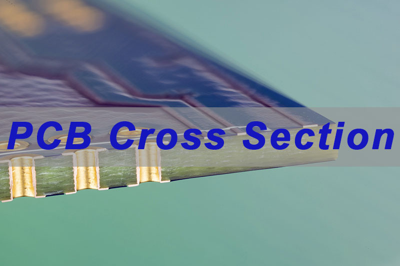
PCB cross section, often referred to as microsectioning, is a critical destructive analysis technique used to inspect the internal structure and quality of a printed circuit board. This article explores the vital role of PCB cross section analysis in ensuring manufacturing integrity, detailing the process, key inspection features, common defects, and why partnering with a specialist is essential for reliable results.
Are you struggling to get definitive answers about your board’s internal quality? Many engineers and manufacturers face these common pain points:
- Inconsistent or unreliable cross-section results from general labs, leading to misdiagnosis.
- Long turnaround times that delay failure analysis and stall production.
- Lack of access to specialized PCB cross section equipment and expertise for complex multilayer boards.
- Unclear PCB cross section reports that fail to pinpoint the root cause of issues like via cracking or delamination.
- Difficulty correlating cross-sectional findings with electrical performance or IPC 6012 requirements.
The solution lies in partnering with a manufacturer that integrates expert PCB cross section services directly into its quality control and failure analysis workflow.
- Guaranteed Precision: We employ a standardized, meticulous PCB cross section procedure performed by certified technicians to ensure consistent, accurate results every time.
- Rapid, Focused Analysis: Our dedicated lab ensures quick turnaround, providing timely insights to keep your projects on schedule.
- Expertise with Advanced Structures: We specialize in analyzing complex builds, including Multilayer PCB cross section and Flexible LED PCB cross sections, using state-of-the-art equipment.
- Comprehensive, Actionable Reporting: Our detailed PCB cross section report includes high-resolution PCB cross section images, clear diagnoses, and actionable recommendations aligned with industry standards.
- Holistic Quality Perspective: As a PCB manufacturer, we interpret findings in the full context of fabrication processes, design, and IPC standards, offering solutions, not just data.
As one of the best PCB manufacturer in China, EBest Circuit (Best Technology) provides expert PCB cross section inspection as a core part of our commitment to delivering high-reliability boards. Our technicians follow stringent protocols to give you an unambiguous view into your product’s integrity. For a definitive analysis of your PCB’s internal quality, pls feel free to contact our team at sales@bestpcbs.com.
What Is PCB Cross Section and Why Is It Used in PCB Quality Evaluation?
PCB cross sectioning is the process of cutting a small, representative sample from a PCB, encapsulating it in resin, grinding and polishing it to a mirror finish, and examining its internal structure under a microscope. It is a foundational tool for quality evaluation because it transforms the board from a 2D layout into a visible 3D model. This allows for direct measurement and assessment of features that are otherwise invisible.
- Verifies Fabrication Accuracy: Confirms critical dimensions like copper thickness, dielectric spacing, and layer registration.
- Validates Material Integrity: Inspects the quality of laminate, prepreg, copper foil, and plating, checking for voids, resin starvation, or imperfections.
- Assesses Plating Quality: Examines the uniformity and completeness of copper plating in via holes and through-holes.
- Supports Failure Analysis: Provides physical evidence for root cause analysis of failures like short circuits, open connections, or intermittent faults.
- Ensures Standard Compliance: Essential for verifying conformance to acceptance standards such as IPC 6012 Class 2/3 or customer-specific requirements.
- Aids in Process Improvement: Identifies manufacturing process deviations, enabling corrective actions.
In summary, PCB cross section analysis is the definitive method for internal inspection, providing irreplaceable empirical data that underpins confident quality evaluation and reliable manufacturing.
How Does PCB Cross Section Analysis Detect Hidden Manufacturing Defects?
A cross section test PCB acts like a medical biopsy, revealing subsurface conditions that electrical tests or visual inspection cannot see. By examining the cross-sectional view, analysts can identify a range of latent defects that compromise long-term reliability.
Key defects detected include:
- Plating Voids in Vias: Empty spaces within the copper barrel of a via, which increase electrical resistance and can cause opens.
- Insufficient Hole Wall Copper: Thin or uneven plating that fails to meet specified thickness requirements, risking current-carrying capacity.
- PCB Delamination: Separation between the copper layer and the laminate or between laminate layers themselves, a critical failure mode.
- Microcracking: Hairline cracks in solder mask, laminate, or copper, often near the knee of a via, which can propagate under thermal stress.
- Etching Issues: Over-etching (under-cut traces) or under-etching (short circuits), visible in the PCB trace cross section profile.
- Solder Mask Overhang: Excessive solder mask covering pad edges, which can interfere with component soldering.
- Drilling Smear: Resin smear left on exposed inner layer copper in a drilled hole, preventing proper plating connection.
This analytical power makes PCB cross section inspection a non-negotiable step for high-reliability applications, catching defects before they lead to catastrophic field failures.
What Steps Are Included in a Standard PCB Cross Section Procedure?
A reliable PCB cross section process follows a precise sequence to ensure the sample truly reflects the PCB’s internal quality. Below is a much cleaner, concise version of the workflow.
Standard PCB Cross Section Steps
| Step | Process | Key Purpose |
|---|---|---|
| 1 | Sample Cutting | Obtain target analysis area |
| 2 | Potting / Encapsulation | Protect sample during grinding |
| 3 | Rough Grinding | Remove bulk material |
| 4 | Fine Grinding & Polishing | Create smooth inspection surface |
| 5 | Microscopic Inspection | Examine internal structures |
| 6 | Optional Etching | Highlight copper grain details |
Sample Cutting
Select a representative area such as a via, trace, or layer stack to ensure meaningful results.
Potting / Encapsulation
Embed the sample in epoxy resin to stabilize fragile edges and prevent layer damage.
Rough Grinding
Use coarse abrasives to quickly approach the target cross-sectional plane.
Fine Grinding & Polishing
Use progressively finer abrasives (down to 1 µm or less) to create a mirror-like surface without scratches.
Microscopic Inspection
Measure and document copper plating, dielectric thickness, voids, cracks, and other structural details.
Optional Etching
Apply chemical etchants when needed to reveal copper grain boundaries or enhance plating evaluation.
A disciplined PCB cross section preparation is essential. Improper grinding, excessive pressure, or poor polishing can create artifacts—such as pulled copper, smeared resin, or rounded edges—that misrepresent the true condition of the PCB. Therefore, expertise in how to cross section PCB samples correctly is critical for reliable analysis.
How Does a Multilayer PCB Cross Section Reveal Layer Structure and Via Integrity?
For complex boards, a multilayer PCB cross section diagram comes to life. It provides a single, comprehensive view of the entire layer stack-up and the interconnections between them. This is invaluable for verifying design implementation and manufacturing execution.
A multilayer PCB cross section inspection focuses on two primary aspects:
A. Layer Stack-up Verification:
- Dielectric Thickness: Measures the thickness of each insulating layer between copper planes.
- Copper Weight/Thickness: Confirms that each signal and plane layer meets the specified ounce/thickness.
- Layer Registration: Checks the alignment of all layers, especially critical for dense designs and via pads.
- Material Integrity: Inspects for voids, foreign inclusions, or signs of degradation in the prepreg and core materials.
B. Via Integrity Analysis:
- Barrel Plating Uniformity: Measures copper thickness at the top, middle, and bottom of the via barrel.
- Inner Layer Capture: Examines the connection between the via plating and the target inner layer pad (the “capture pad” or “annular ring”).
- Multilayer PCB Cross Section Via Connect: Specifically assesses the quality of connections in buried or blind vias, which are only visible internally.
- Knee Cracking: Looks for cracks at the junction where the via barrel meets an inner layer, a common failure point under thermal stress.
By analyzing these elements, engineers can validate that the cross section of PCB matches the intended design and possesses the mechanical robustness for its application.
What PCB Cross Section Equipment Is Required for Accurate Microsectioning?
The accuracy of a PCB cross section analysis is directly tied to the quality of the equipment used. A professional lab requires a specific PCB cross section equipment list to perform reliable microsectioning.
- Precision Sectioning Saw: For clean, precise cutting of the sample area without damaging adjacent features.
- Mounting/Pressing Press: To properly encapsulate the sample in epoxy resin under controlled pressure and temperature.
- Grinder/Polisher Machine: An automated system with variable speed for consistent, sequential grinding and polishing steps. This is often a central piece of PCB cross section equipment.
- High-Resolution Metallurgical Microscope: Equipped with brightfield/darkfield illumination and high-magnification objectives (50x, 100x, 200x, 500x) for detailed inspection.
- Digital Imaging System: A high-quality camera and software attached to the microscope for capturing, measuring, and annotating PCB cross section images.
- Precision Measurement Tools: Stage micrometers and software calibration for accurate dimensional analysis (e.g., measuring cross sectional area of PCB trace).
Investing in high-caliber equipment like Leica cross section microscopes and precision polishing systems minimizes preparation artifacts and ensures that the observed details are true board features, not preparation errors.
What Can Engineers Identify From a PCB Via Cross Section During Failure Analysis?
The PCB via cross section is one of the most critical tools in failure analysis. Engineers use it to detect hidden structural issues that directly affect reliability.
Common Via Defects
| Defect | Visual Indicator | Impact |
|---|---|---|
| Plating Void | Empty spot in barrel | Open / high resistance |
| Nail Heading | Copper bulging | Short risk / uneven surface |
| Insufficient Plating | Thin copper barrel | Crack risk / low current |
| Resin Smear | Resin covering inner pad | Inner layer disconnect |
| Knee Crack | Crack at via corner | Intermittent / open circuit |
| Poor Wetting | Poor copper adhesion | Weak bond / instability |
Plating Void
Indicates a cavity in the via barrel; may cause open circuits under load.
Nail Heading
Copper extrusion at drill entry/exit; may create shorts or planarity issues.
Insufficient Plating
Weak, thin copper; highly vulnerable to thermal cycling cracks.
Resin Smear
Resin left on inner layer pads; prevents proper electrical connection.
Knee Crack
Cracks at the via knee; often intermittent and triggered by thermal stress.
Poor Wetting
Inadequate copper bonding; weak connection and long-term instability.
Why This Matters
By correlating cross section results with electrical data and stress conditions, engineers can identify whether the root cause is related to:
• drilling
• desmear
• plating
• material performance
• thermal/mechanical stress
This leads to accurate and actionable corrective actions.
What Key Features Do Engineers Inspect in a Standard PCB Cross Section?
A thorough PCB cross section inspection follows a checklist to ensure all critical quality parameters are assessed. A comprehensive PCB cross section report will include data and images related to these key features.
- Copper Features:
- Trace Width/Spacing: Verification against design specifications.
- Copper Thickness: For outer layers and inner layers, measured from the PCB trace cross section.
- Plating Thickness: Of via barrels, pads, and any surface finish (e.g., ENIG, HASL).
- Profile: Sidewall angle after etching (should be trapezoidal, not under-cut).
- Dielectric Features:
- Dielectric Thickness: Between each layer pair in the stack-up.
- Laminate & Prepreg Integrity: Absence of voids, glass weave distortion, or resin starvation.
- Interconnection Features:
- Annular Ring: The amount of copper pad extending beyond the drilled hole, for both outer and inner layers.
- Via Fill: For filled vias, the completeness and quality of the fill material (epoxy, conductive paste, copper).
- Solder Mask: Thickness, coverage over traces, and registration over pads.
- Material Interface Integrity:
- Adhesion: No signs of PCB delamination between copper and laminate or between laminate layers.
- Plating Adhesion: Strong bond between electroplated copper and base copper.
Inspecting these features against the relevant PCB cross section standard (like IPC-TM-650 2.1.1) provides a quantifiable measure of manufacturing quality and process control.
In conclusion, PCB cross section analysis remains an indispensable technique for achieving and verifying high-quality PCB manufacturing, acting as the ultimate diagnostic tool for internal integrity. This article has detailed how this process uncovers hidden defects, validates complex structures, and guides failure analysis.
For manufacturers and designers who cannot afford hidden flaws, accessing expert PCB cross section services is crucial. EBest Circuit (Best Technology) provides this critical capability in-house, combining state-of-the-art PCB cross section equipment with deep manufacturing expertise. We ensure your boards are built to last, from the inside out. To discuss your project’s quality assurance needs, please contact us at sales@bestpcbs.com.