

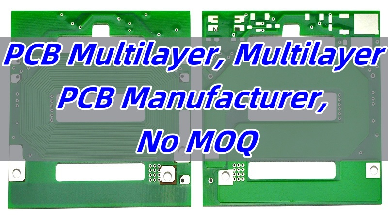
Multilayer PCB manufacturer is one of the most searched terms by engineers and procurement teams today. These boards are the backbone of modern electronics. Whether it’s a medical scanner or a mobile phone, you’ll likely find a multilayer board inside. But who builds these PCBs? How are they made? And most importantly, who can you trust to deliver quality boards every time? Let’s explore all the key points to help you choose the right manufacturer.
As a well-established multilayer PCB manufacturer, EBest Circuit (Best Technology) is committed to providing the turnkey electronic circuit solution to our global customers. In EBest Circuit (Best Technology), we not only focus on domestic business but the global market. The export sales account for 90% of our total sales. With above 18 years of experience, we recommend the PCB design, material sourcing, and manufacturing processes for our customers. We build the multilayer PCB manufacturing and assembly in one house, which gives us access to provide the PCBs in a more stable quality, at a lower cost, and a shorter lead time. For any multilayer PCB manufacturing technique questions or any multilayer PCB project demands, kindly reach out to us at sales@bestpcbs.com for support.
What is the best multilayer PCB manufacturer?
The best multilayer PCB manufacturer doesn’t just deliver on-time. They offer consistent quality, engineering support, and technical clarity. When looking at top players globally, a few key traits stand out:
- Advanced production capabilities (like laser drilling and AOI systems)
- Strong quality assurance with certifications
- Flexible lead times for prototyping and mass production
- Real support from real engineers, not chatbots
Companies like EBest Circuit (Best Technology) excel by focusing on clear communication, competitive pricing, and precision manufacturing. We don’t just push products; we solve problems.
Who manufactures multilayer PCB?
Multilayer PCBs are manufactured by specialized facilities with tight process control. EBest Circuit (Best Technology) is a multilayer PCB manufacturer. We have our PCB manufacturing & SMT factories. There is sophisticated machinery in our PCB Manufacturing Plants, such as:
- Multilayer PCB prototyping machines
- Lamination presses
- Flying probe testers
- X-ray inspection systems
Our multilayer PCBs are applicable in all walks of life, like consumer electronics, aerospace, medical, or industrial applications. We can support the complex multilayer PCBs, especially in server and high-speed computing systems. You can enjoy the quick turn prototyping service and our multiple-to-one support. For any multilayer PCB project, kindly contact us at sales@bestpcbs.com for a tailored service.
Multilayer PCB manufacturers in India
India is becoming a global hotspot for electronics manufacturing. So, it’s no surprise that many reliable multilayer PCB manufacturers have emerged across the country. These companies support various industries, including automotive, telecom, consumer electronics, and defense. If you’re sourcing PCBs from India, knowing the best options can help you make an informed decision.
Here are three well-known multilayer PCB manufacturers in India:
1. AT&S India
- AT&S is a global leader with a manufacturing base in Nanjangud, Karnataka. The company produces high-quality multilayer PCBs for automotive and industrial use. Their Indian plant specializes in high-end HDI and multilayer boards. It is part of their broader strategy to support Asia-Pacific customers with fast lead times and consistent quality.
2. Shogini Technoarts
- Located in Pune, Shogini Technoarts has been delivering PCBs for over four decades. They manufacture single-sided, double-sided, and multilayer PCBs. Their key strength lies in serving sectors like lighting, telecom, and industrial automation. They’re known for their cost-effective production and excellent customer service.
3. Genus Electrotech
- Genus Electrotech operates one of the largest PCB manufacturing plants in India. Based in Gandhinagar, Gujarat, they produce multilayer PCBs with a strong focus on quality assurance. Their products are widely used in consumer electronics, energy meters, and home appliances. They offer end-to-end solutions from PCB design to assembly.
India’s multilayer PCB industry is growing rapidly. Companies like AT&S India, Shogini Technoarts, and Genus Electrotech offer solid options if you’re looking for quality and reliability. Depending on your industry, budget, and product requirements, each of these firms can be a valuable partner.
How is multilayer PCB manufactured?
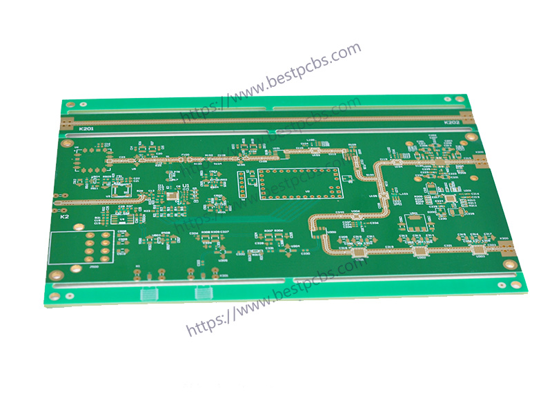
Multilayer PCB manufacturing is a detailed process that requires strict control and precision. At EBest Circuit (Best Technology), we follow a refined and efficient workflow to ensure the best outcomes for every board we produce. Here’s a breakdown of our process for a four-layer PCB:
1. Material Cutting
- We begin by cutting the raw laminate material into required panel sizes. This step sets the base size for the board and prepares it for inner layer processing.
2. Inner Layer Circuit
- We print the inner circuit using photoresist exposure, development, and etching. This creates the copper traces on the inner layers.
3. AOI (Automated Optical Inspection)
- Each inner layer goes through AOI to detect any defects. This ensures the circuit patterns are correct before lamination.
4. Lamination
- The cleaned inner layers and prepregs are stacked and laminated under heat and pressure. This bonds the layers together into one solid board.
5. Drilling
- Next, we drill holes to create vias that will connect the layers. Precise drilling is critical for multilayer connectivity.
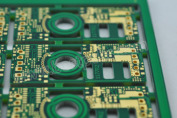
6. Copper Deposition & Plating
- We apply a thin layer of copper into the holes through chemical deposition. Then, we electroplate the whole panel to thicken the copper and improve conductivity.
7. Outer Layer Circuit
- Just like the inner layers, we form the outer circuit by exposing, developing, and etching. This step defines the top and bottom copper traces.
8. Outer Layer AOI
- We inspect the outer circuit layers using AOI to catch any missing connections or short circuits.
9. Solder Mask
- A protective solder mask is applied to prevent oxidation and short circuits during assembly. We expose and develop it to open pads and vias.
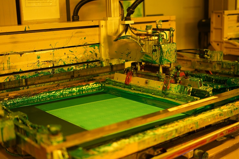
10. Silkscreen
- We print labels, logos, and part identifiers on the PCB using silkscreen printing.
11. Baking
- The board is baked to cure the solder mask and silkscreen layers. It also removes moisture from the board.
12. Surface Finish
- We apply surface finishes such as ENIG, HASL, or OSP depending on customer requirements. This prepares the pads for soldering.
13. Profiling
- The PCB is routed or punched to its final shape. Any sharp edges or burrs are removed.
14. Electrical Testing
- Each PCB undergoes electrical testing to check for open and short circuits. We verify continuity across all connections.
15. Final Quality Check (FQC)
- Our FQC team checks appearance, dimensions, and mechanical properties. They ensure every board meets client standards.
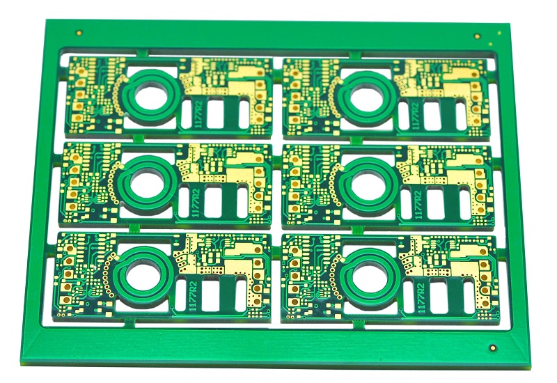
16. Packing & Storage
- Boards are packed using anti-static materials and barcoded for traceability. They are then stored safely for shipping.
In conclusion, this process ensures high yield and consistent performance. At EBest Circuit (Best Technology), we rely on detailed checks at every stage to maintain quality. That’s how we deliver reliable multilayer PCBs for industries like medical, automotive, and telecom.
Why are there no 3-layer PCBs?
Ever noticed how PCBs are mostly 2, 4, 6, or 8 layers? That’s because PCBs are stacked in pairs. Laminating an odd number like 3 is not practical.
Stackups need to be balanced. An uneven layer count causes warping during lamination. That’s why if you need 3 layers of routing, you’ll get a 4-layer board. The extra layer keeps it flat and stable.
How to choose a multilayer PCB manufacturer?
Selecting the right supplier saves time, cost, and headaches. Here’s what you should check:
1. Certifications
Look for ISO9001, IATF16949 (automotive), AS9100D (aerospace), and ISO13485 (medical).
2. Engineering Support
Can they help with stackup design or impedance control?
3. Lead Time
Are they fast enough for your project deadlines?
4. Manufacturing Equipment
Check if they have AOI, flying probe, and automated plating systems.
5. Material Options
Can they source Rogers, FR4, or halogen-free materials?
6. Traceability
Do they offer MES systems to track every batch?
A good multilayer PCB manufacturer will openly share these details. If they hesitate, that’s a red flag.
Why should you choose EBest Circuit (Best Technology) as your trusted multilayer PCB manufacturer?
EBest Circuit (Best Technology) offers all the right reasons to be your go-to multilayer PCB manufacturer.
- Advanced Capabilities: We handle 4 to 40-layer boards with HDI, impedance control, and via-in-pad.
- Certified Quality: Our factory meets ISO9001, ISO13485, IATF16949, and AS9100D.
- Strong Engineering Support: We guide your stackup, drill charts, and impedance planning.
- Smart Systems: Our MES tracks every component or full traceability.
- Testing Assurance: Flying probe, X-ray, ICT, and functional testing ensure zero-defect output.
- Fast Delivery: Prototypes in 3–5 days. Mass production in about 14 days.
Customers across automotive, telecom, and medical industries trust us. We don’t just make PCBs. We deliver the solution for all series of PCBs.
To sum up, finding the right multilayer PCB manufacturer isn’t about price alone. It’s about trust, support, and consistent quality. You want a partner who gets your design, meets your deadlines, and keeps your product running smoothly.
EBest Circuit (Best Technology) has the tools, team, and track record to help your projects succeed. From complex stackups to mass production, we have the professional talents and the sophisticated technology to get you covered. Do you want to get a quote for PCB Multilayer? Just send your Gerber files, quantity, and specs to us at sales@bestpcbs.com. You’ll get a favorable quote in 24 hours. And there is no MOQ in EBest Circuit (Best Technology).