

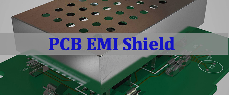
PCB EMI shield refers to a grounded metal shielding structure—typically a frame-and-lid or formed can—used to contain radiated emissions and improve immunity on dense PCBAs. This article explains how EMI shielding works on a PCB, how to design and integrate shields without hurting SMT yield or test access, and how to choose the right shield structure for high-density builds.
When an EMC issue shows up late—after layout is “done” and prototypes are already on the bench—what are the most common problems teams run into with shielding on real PCBAs?
- Emissions fail late, and the fix becomes a mechanical scramble.
- Shield soldering causes tombstoning, warpage, or opens.
- Test points get blocked, slowing debug and production test.
- Rework becomes risky or impossible after the lid is installed.
- Shield seams leak, so the “fix” barely moves the EMC needle.
A reliable approach is to treat shielding as a PCBA-integrated system—layout, grounding, soldering, and test strategy working together.
- We select shield structures that match the assembly flow and rework needs.
- We design footprints and paste patterns to stabilize solder joints.
- We engineer ground paths to avoid slot antennas and seam leakage.
- We protect test access with deliberate windowing and test planning.
- We validate performance with repeatable build notes and inspection controls.
EBest Circuit (Best Technology) is a one-stop PCB fabrication and turnkey PCBA assembly manufacturer supporting high-density, high-reliability builds across demanding industries. Our engineering team focuses on DFM-first shielding integration—footprint design, SMT sequencing, and test accessibility—so your PCBAs pass EMI requirements without sacrificing yield or serviceability. If any questions, pls feel free to contact us at sales@bestpcbs.com.
What Is a PCB EMI Shield and Why It Matters in High-Frequency Electronic Designs?
A PCB EMI shield is not just a “metal box.” In high-frequency, high-density PCBA layouts, shielding becomes a controlled boundary that manages where fields can couple, where return currents flow, and how sensitive circuits survive near noisy sources.
Key Roles a PCB EMI Shield Plays
- Contain radiated energy from clocks, switching power, and high-speed interfaces.
- Reduce susceptibility by protecting sensitive RF, analog, or sensor nodes.
- Control coupling paths between adjacent subsystems on dense assemblies.
- Stabilize EMC outcomes when board-level changes are limited late in NPI.
- Enable compartmentalization on mixed-signal designs.
Quick Reference Table: Where Shields Usually Add the Most Value
| Scenario | Why Shielding Helps | Typical Shield Type |
|---|---|---|
| Noisy digital near RF | Limits near-field coupling | Frame + lid |
| Switching power near sensors | Reduces magnetic/electric coupling | Can with strong grounding |
| Mixed-signal dense PCBA | Creates functional isolation | Multi-compartment shield |
| Layout can’t change | Adds an external control boundary | Retrofit can |
A shield matters most when frequency rises, spacing shrinks, and the PCBA becomes an ecosystem of interacting fields rather than “separate blocks.”
How EMI Shielding in PCB Works to Reduce Radiation and Susceptibility Issues?
EMI shielding in PCB works by creating a low-impedance reference boundary that redirects displacement currents, reduces fringing fields, and minimizes unintended antenna behavior from structures and seams.
What Actually Makes Shielding Work
- Conductive enclosure effect: fields prefer to terminate on a grounded conductor rather than radiate.
- Return-path control: a good ground connection reduces loop area and radiation.
- Seam management: leakage often happens at gaps, lid seamss, and poor contact points.
- Compartment isolation: separating circuits reduces cross-coupling between aggressors and victims.
- Absorption vs reflection: material, thickness, and frequency determine which dominates.
Practical Note for High-Density PCBA
- A shield that is “electrically floating” behaves unpredictably.
- A shield with weak ground contact can become part of the antenna.
At production scale, EMI shielding in PCB is less about theory and more about controlled grounding, seam discipline, and consistent assembly execution.
Key Principles of PCB EMI Shielding Design for Signal Integrity and Compliance
PCB EMI shielding design succeeds when you design the footprint, grounding, and keep-outs as a system—then align it with SMT realities so the shield lands consistently across volume builds.
Core Principles That Prevent “Shield-Added, EMC-Still-Fails”
- Define the shield boundary early: decide what is inside vs outside the compartment.
- Create a continuous ground ring: avoid fragmented ground that creates slots.
- Control stitch via spacing: reduce inductance along the perimeter.
- Manage apertures intentionally: vents and openings must be deliberate, not accidental.
- Protect critical return paths: do not force high-speed returns to detour.
- Plan test and rework access: shielding that blocks debug adds schedule risk.
Compact Checklist (DFM-First for PCBA)
- Keep a clear solderable land pattern around the shield perimeter.
- Avoid solder mask slivers that break continuity at the ground ring.
- Reserve removal strategy if rework is a realistic requirement.
The best PCB EMI shielding design reduces iterations by preventing the usual “fitment + solderability + seam leakage” loop.
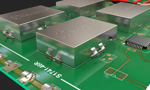
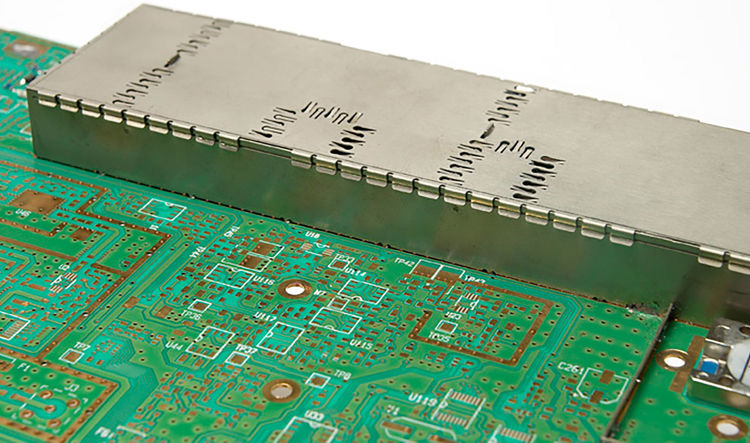
Common Structural Types of PCB EMI Shield Frame and Lid Assemblies
PCB EMI shield frame and lid structures are popular because they balance shielding performance with serviceability—when the footprint and assembly sequence are designed correctly.
Common Structure Types You’ll See in Production
- Two-piece frame + removable lid: good for tuning and rework.
- One-piece formed can: simpler assembly, often faster for volume.
- Clip-on lid variants: improves re-openability but demands precise frame geometry.
- Gasketed lids: improves seam sealing in some frequency ranges.
- Multi-bay frame + lid: compartmentalizes multiple functional blocks.
Fast Comparison Table (PCBA Reality)
| Type | Strength | Risk | Best Use |
|---|---|---|---|
| Frame + lid | Rework-friendly | Seam leakage if contact weak | RF tuning, debug-heavy |
| One-piece can | Simple | Harder rework | Stable production |
| Multi-bay | Strong isolation | Footprint complexity | Dense mixed-signal |
For high-density PCBA, the “best” structure is the one that survives SMT, preserves test access, and still controls leakage at seams.
Design Considerations for PCB EMI Shielding Cover and Frame Integration
PCB EMI shielding cover and frame integration should be treated as an assembly feature, not only an EMC feature. The footprint, paste design, and grounding continuity determine whether the shield is reliable in volume.
Integration Decisions That Affect Yield and EMC Together
- SMT sequencing: frame placement timing vs nearby fine-pitch components.
- Paste pattern strategy: avoid float, tilt, and solder void concentration.
- Coplanarity and warpage tolerance: metal parts can amplify uneven solder joints.
- Ground contact continuity: maximize consistent contact around the perimeter.
- Keep-outs and component height: prevent mechanical interference and lid shorting.
- Test access planning: reserve windows or removable lid strategy for debug.
Practical “Do This, Not That” Table
| Goal | Do This | Avoid This |
|---|---|---|
| Stable soldering | Segment paste openings | Full continuous paste ring |
| Strong grounding | Stitch vias on ring | Sparse vias and broken ground |
| Rework-ready | Removable lid plan | Permanent lid with blocked access |
Done well, cover and frame integration improves EMC without turning PCBA into a rework dead-end.
When to Use a PCB Mount EMI Shield or Multi-Compartment Shielding Solution
A PCB mount EMI shield is appropriate when the board-level layout cannot deliver enough separation, and you need repeatable isolation across builds. Multi-compartment solutions are best when multiple aggressor/victim pairs share a tight area.
Use a PCB Mount EMI Shield When
- You need quick EMC improvement without major reroute.
- RF/analog nodes sit close to fast digital clocks.
- Power switching noise couples into sensitive measurement circuits.
- The product has a known “noisy corner” that repeats across revisions.
Use a PCB Multi-Compartment EMI Shield When
- Multiple blocks need isolation inside the same physical footprint.
- Shared ground paths create cross-coupling between subsystems.
- You need predictable EMC behavior across variants of the same PCBA.
- Mechanical enclosure shielding is insufficient or inconsistent.
Mini Decision Matrix
| Constraint | Best Fit |
|---|---|
| One hot-spot area | PCB mount EMI shield |
| Multiple mixed blocks | PCB multi-compartment EMI shield |
| Heavy debug/rework | Removable lid approach |
Choosing the right shield architecture reduces both EMI risk and assembly complexity—especially on dense builds.
Custom EMI PCB Shield Options for Irregular Layouts and High-Density Boards
A custom EMI PCB shield is often the only practical choice when your layout has non-rectangular keep-outs, uneven component heights, or tight mechanical envelopes that standard cans cannot accommodate.
When Custom Shields Deliver Real Value
- Irregular footprints: curved boundaries, angled edges, or dense connector zones.
- Height variation: tall components inside a low-profile mechanical envelope.
- Thermal constraints: balancing shielding with heat dissipation paths.
- Mechanical constraints: enclosure bosses or stiffeners near the shield boundary.
- Serviceability needs: lids designed for repeatable removal without pad damage.
“Rectangular vs Custom” Snapshot
- emi shield for pcb rectangular works well for uniform block layouts and predictable keep-outs.
- custom emi pcb shield fits when density and mechanics force non-standard geometry.
In PCBA, custom shields become most successful when the footprint, assembly sequence, and inspection notes are defined as clearly as the shield geometry itself.
Typical Applications and Selection Guidelines for PCB EMI Shields in Modern Electronics
PCB EMI shields are common in products where dense integration, high-speed interfaces, and mixed-signal blocks make “layout-only” EMI control impractical.
Typical Applications
- Wireless modules and RF front ends.
- High-speed compute with dense clocks and DDR interfaces.
- Industrial sensing with low-level analog measurement.
- Medical electronics requiring stable immunity performance.
- Automotive modules where EMI constraints are aggressive.
Selection Guidelines That Work in the Real World
- Define the noise source and victim clearly before choosing structure.
- Choose the simplest shield that achieves the EMC target.
- Prioritize ground continuity and seam control over “thicker metal.”
- Confirm test access and rework path early.
- Align the shield choice to your assembly line’s repeatability.
PCB EMI shields are most effective when they are selected as part of a manufacturing plan—not as a last-minute add-on.
PCB EMI shield integration creates a grounded boundary that helps high-density PCBAs control emissions and improve immunity when spacing is tight and frequencies are high. This article covered how shielding works on a PCB, practical PCB EMI shielding design principles, frame-and-lid structures, cover and frame integration, multi-compartment selection, and custom shield options for dense layouts. EBest Circuit (Best Technology) supports reliable shielding integration through DFM-first footprints, controlled SMT sequencing, and build-ready documentation that protects yield and testability. For more information or if you would like to send us any inquiry, please send us an email through the contact form at the bottom of our Contact Page.
FAQs
What Is a PCB Shield?
A PCB shield is a conductive barrier—often a metal can or frame-and-lid assembly—grounded to the PCB to reduce radiated emissions and improve immunity for sensitive circuits.
How to Avoid EMI in PCB?
Use short return paths, minimize loop area, control impedance where needed, segment noisy and sensitive blocks, and apply shielding only after grounding and layout fundamentals are correct.
What Causes EMI in PCB?
Common causes include fast edge rates, large current loops, poor return paths, inadequate decoupling, uncontrolled impedance discontinuities, and unintended antenna structures such as long traces or seams.
Can Aluminum Foil Shield EMI?
Aluminum foil can reduce some near-field coupling in a lab setup, but it is not a controlled, repeatable production solution because grounding, seam control, durability, and safety are difficult to guarantee on PCBAs.