Looking for custom PCB design and fabrication services? This guide covers services, processes, DFM principles and quotes to help you find reliable custom solutions.
What Is PCB Designing and Fabrication?
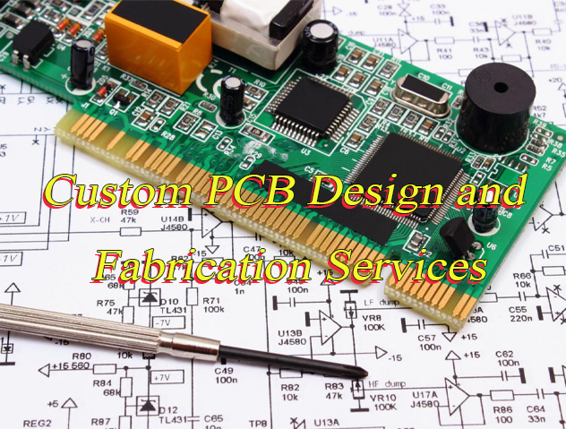
PCB designing and fabrication transforms an electronic concept into a reliable, build-ready circuit board through a tightly connected engineering process. It begins with schematic design and layout planning, where signal paths, power flow, and component placement are carefully arranged. From there, the design is converted into precise manufacturing data that guides copper etching, layer lamination, drilling, and surface finishing. When design intent and fabrication capability are aligned early, the result is a board that performs as expected and moves smoothly into assembly.
At the same time, successful PCB designing and fabrication depends on practical decisions, not just electrical theory. Material selection, stack-up balance, and manufacturability checks all play a role in controlling cost and quality. Clear documentation and early DFM reviews help avoid rework and schedule delays. By treating design and fabrication as one continuous workflow, teams can achieve faster turnaround, higher yield, and more predictable production outcomes.

Types of Custom PCB Design and Fabrication Services
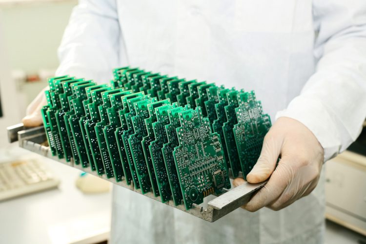
Custom PCB design and fabrication services cover diverse project needs, with specialized options for every stage. Prototype services handle low-volume orders (1-100 units) for design validation. They offer fast turnaround (24-72 hours) to speed up your testing cycles and allow quick iterations.
Small-batch fabrication (100-5,000 units) balances speed and cost. It suits niche products or pre-market launches, with flexible surface finishes and material choices. High-volume production (5,000+ units) uses automated workflows for consistency and efficiency, ideal for mass-market products.
Additionally, specialized services cater to complex needs. These include HDI (High-Density Interconnect) boards for compact devices and high-frequency PCBs for RF applications. Rigid-flex PCBs and automotive-grade options (compliant with IATF 16949) are also available for targeted industries.
PCB Design and Fabrication Process
Below are PCB design and fabrication process for your reference:
1. Design Phase: Schematic Capture & Layout
- Schematic Design: Begin with accurate schematic creation using tools like Altium Designer, OrCAD, or KiCad. Ensure component libraries adhere to IPC standards for consistency.
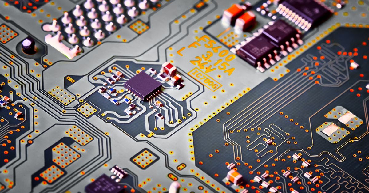
- PCB Layout: Translate schematics into a physical layout, prioritizing signal integrity (e.g., controlled impedance routing, minimizing EMI via proper ground planes). Use design rule checks (DRC) to validate clearance, trace width, and differential pair spacing.
- Advanced Techniques: For HDI designs, incorporate microvias (0.1mm or smaller) and blind/buried vias to optimize space. Flexible PCBs require specialized material selection and bend-radius calculations.
2. Material Selection & Stackup Design
- Substrate Materials: Choose FR-4 for cost-effective rigid boards, polyimide for flex circuits, or high-frequency laminates (e.g., Rogers RO4350B) for RF applications. Consider thermal management needs with materials like aluminum-core boards.
- Copper Weight & Thickness: Select copper weights (0.5oz to 4oz) based on current-carrying requirements. Thicker copper enhances thermal dissipation but increases cost.
- Stackup Configuration: Define layer count and sequence (signal, power, ground layers) to minimize crosstalk. Use symmetric stackups for warpage control during fabrication.
3. Imaging, Etching & Plating
- Photolithography: Apply photoresist, expose to UV through artworks, and develop to create circuit patterns. Modern LDI (Laser Direct Imaging) eliminates film usage, enhancing precision.
- Etching: Use ammonia-based etchants for copper removal, ensuring precise trace edges. Acid-copper plating follows to deposit thick copper in vias and pads.
- Via Processing: Mechanical drilling for standard vias; laser drilling for microvias. Copper plating via holes ensures electrical continuity.
4. Surface Finish & Solderability
- HASL (Hot Air Solder Leveling): Traditional tin-lead or lead-free finish for through-hole components.
- ENIG (Electroless Nickel Immersion Gold): Ideal for fine-pitch SMT pads, wire bonding, and aluminum wire connections. Provides excellent shelf life.
- OSP (Organic Solderability Preservative): Cost-effective for short-term storage, but less durable than ENIG.
- Immersion Silver/Tin: For high-frequency applications to maintain signal integrity.
5. Drilling, Routing & Mechanical Processing
- CNC Drilling: Precision drilling of via holes and mounting holes. Use peck drilling to prevent tool wear.
- Routing & Profiling: CNC routing machines cut board outlines and internal slots. V-scoring enables easy separation of panelized boards.
- Beveling & Countersinking: Chamfer edges for assembly safety; countersink holes for flush screw heads.
6. Inspection, Testing & Quality Assurance
- AOI (Automated Optical Inspection): Detects solder mask defects, missing pads, and trace misalignment.
- X-ray & CT Inspection: For hidden defects like voids in BGA solder joints or buried via integrity.
- Electrical Testing: Flying probe or in-circuit testers verify connectivity. Use netlist comparison to catch opens/shorts.
- Environmental Testing: Thermal cycling, humidity testing, and vibration tests ensure reliability under operational conditions.
7. Assembly Integration & Soldering
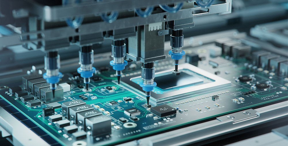
- SMT (Surface Mount Technology): Stencil printing, pick-and-place machines, and reflow ovens assemble dense components. Nitrogen reflow reduces oxidation.
- Through-Hole Assembly: Wave soldering for traditional components; selective soldering for mixed-technology boards.
- Conformal Coating: Protect against moisture, dust, and chemicals. Acrylic, silicone, or parylene coatings are common.

DFM Principles to Optimize PCB Design for Fabrication
- Keep trace widths and spacing consistent: Use 6mil/6mil minimum for standard boards and 3mil/3mil for HDI, with ±10% tolerance for precision. HDI designs typically add 15%-20% to production costs.
- Route traces at least 12mil away from chip pads: Maintain ≥2mil green oil bridges between pads to prevent soldering defects during assembly.
- Standardize hole sizes to 0.15mm-1.0mm range: Control non-plated hole tolerance at ±2mil to reduce tooling changes and cut drilling time by 30%.
- Maintain 12mil distance between vias and pads: Use square board edges and 3mm clearance from components, with ≥1mm rounded corners for stability.
- Use 45 or 90-degree angles for traces near pads: Avoid angles below 30 degrees, as they trap acid and accelerate copper corrosion after 30+ hours in humid environments.
- Add test points early with 1.0mm-1.2mm diameter: Space them ≥70mil apart and keep 125mil clearance from board edges for post-assembly testing.
- Incorporate DFM reviews within 24 hours of design finalization: These checks reduce rework risks by 30%+ and align layouts with fabrication capabilities upfront.

Material Selection Strategies for Custom PCB Design and Fabrication
Material selection directly impacts PCB performance and production efficiency. PCB design and fabrication relies heavily on proper material matching, so follow these targeted strategies:
- General-purpose projects choose FR-4: Optimize for UL94 V-0 flame-retardant grades with Tg 130-140℃. Its Dk 4.2-4.8 (1MHz) and Df 0.020-0.025 fit consumer electronics and industrial controls.
- High-frequency (1GHz+) use specialized substrates: Pick PTFE or Rogers materials for stable Dk values and minimal signal loss. RO5880 suits 77GHz automotive radar; RO3003 works for GPS and base station antennas.
- High-temperature applications need high-Tg substrates: Select variants with Tg ≥150℃ to resist reflow soldering deformation. High-multilayer boards require Tg 170-180℃+ for industrial and automotive use.
- Match surface finishes to assembly needs: ENIG (4-8μm nickel, 0.05-0.1μm gold) fits fine-pitch components and long storage. HASL offers cost-effectiveness for general use; OSP suits lead-free tight-pitch designs.
- Adapt to harsh environments: Use high-CTI FR4 for high-voltage moist settings. Prioritize materials with strong thermal conductivity for high-power or extreme-temperature scenarios.
- Align with impedance control goals: For 50Ω/75Ω impedance requirements, coordinate substrate Dk with trace width and dielectric thickness. This ensures signal integrity in high-speed designs.
Quality Control and Testing Methods in PCB Design and Fabrication
Strict quality control (QC) guarantees consistent, reliable PCB design and fabrication results. Implement these targeted testing methods for comprehensive validation:
- Flying Probe Electrical Testing: Check for open/short circuits with 95%+ coverage. Maintain contact resistance below 10mΩ for accurate results across all layers.
- TDR Impedance Testing: Control impedance tolerance within ±10% for high-frequency boards. Narrow to ±7% for 5G and DDR fast-data applications to preserve signal integrity.
- AOI Visual Inspection: Use automated optical equipment to detect 0.05mm micro-defects. Catch trace blemishes, solder joint issues and component misalignment per IPC-A-600 standards.
- Thermal Cycling Testing: Subject boards to 40℃ below zero to 125℃ cycles. Complete 3 rounds of 288℃ solder dipping for 10 seconds each to test temperature resistance.
- Humidity Cycling Testing: Validate stability in moist conditions. Run 85℃/85%RH cycles for 1000 hours to ensure no layer separation or insulation degradation.
- Ion Contamination Testing: Keep post-fabrication residue below 5μg/in². Use eco-friendly cleaning agents to prevent corrosion and extend board lifespan.

Common Pitfalls & Solutions in PCB Design and Fabrication
Pitfall 1: Pad and Aperture Mismatch. This causes drill breakage and circuit defects.
Solution 1: Use DRC tools to validate coordinates early. Control aperture tolerance at ±2mil, standardize pad markings and set pad size 0.2mm larger than hole diameter.
Pitfall 2: Unclear Layer Stackup. This triggers signal interference and EMI.
Solution 2: Label layers sequentially and keep signal layers adjacent to ground planes. Design even-layer stacks symmetrically to prevent high-temperature deformation.
Pitfall 3: Inadequate Component Spacing. This leads to soldering flaws and thermal issues.
Solution 3: Maintain ≥0.5mm minimum spacing. Keep high-power devices 5mm+ from precision components and use differential pair routing for high-speed signals.
Pitfall 4: Incomplete Gerber Files. This results in misfabrication.
Solution 4: Export RS-274X format files covering all layers. Conduct pre-fabrication reviews with your provider to verify data integrity before production.
Pitfall 5: Asymmetric Layer Lamination. This causes board warpage after reflow.
Solution 5: Adopt symmetric stackup for even-layer boards. Add dummy copper to balance stress for odd-layer designs and match material thermal expansion coefficients.
Pitfall 6: Poor High-Speed Signal Routing. This degrades signal integrity.
Solution 6: Route differential pairs with consistent 50Ω/75Ω impedance. Keep pair spacing 3-5mil and avoid sharp bends to reduce noise interference.
Why Choose EBest(Best Technology) for Custom PCB Design and Fabrication Partner?
Reasons why choose EBest(Best Technology) for custom PCB design and fabrication partner:
- 19 Years of Professional Expertise: We’ve specialized in custom PCB production since 2006, serving over 4000 global clients. Having delivered more than 1.2 million custom PCBs, we cater to high-end sectors like aerospace, automotive and medical.
- 24-Hour Rapid Prototyping and Delivery: 1-8 layer standard PCB prototypes ship within 24 hours, including full electrical testing and AOI inspection. Small-batch orders (100-500 units) deliver in 48 hours with a 99.2% on-time rate to speed up your project cycles.
- Sample & Small-Batch Customization Capacity: Support 1-piece sample orders and 1-5000 units small-batch customization. Custom types cover 1-24 layer boards, HDI, ceramic PCBs, rigid-flex and automotive/medical-grade options with full parameter tailoring.
- Strict Quality Control with Authoritative Certifications: Boast ISO9001, AS9100D (aerospace) and IATF 16949 (automotive) certifications. Execute 18 rigorous QC processes to keep product yield consistently above 99.5%.
- One-Stop PCBA Custom Services: Offer integrated custom PCB fabrication, BOM procurement, SMT assembly (precision ±0.03mm) and functional testing. Tailor solutions to cut multi-party communication costs and streamline workflows.
- MES System for Full-Process Traceability: Track production nodes, process parameters and inspection data in real time via MES. Enjoy end-to-end batch traceability with 3 years of data retention for compliance and accountability.
- Flexible Customized Solutions: Adapt processes to meet special requirements like high-voltage ceramic PCBs and ultra-thin HDI boards. Offer 1-on-1 technical consultation to optimize custom designs and accelerate project success.
Welcome to contact us if you have any request for PCB design and fabrication services: sales@bestpcbs.com.


