

Copper thickness on PCB plays a major role in the performance, reliability, and thermal management of electronic circuits. Whether you’re developing a simple controller or a power-hungry inverter, the right copper thickness ensures your board handles the load efficiently and safely.
EBest Circuit (Best Technology) is an integrated manufacturer, providing a broad services like material procurement, PCB prototype, PCB mass production, turnkey assembly, and box building in the Chinese market and the international market. Our PCB product lines include extra-thin PCB, heavy copper PCB, HDI PCB, high frequency PCB, and high speed PCB. If you require the detailed quote for custom copper thickness on PCB, or PCB copper plating thickness, please let us know at sales@bestpcbs.com.
What is Copper Thickness on PCB?
Copper thickness on PCB refers to the amount of copper applied to the board’s surface and inner layers. It’s usually measured in ounces per square foot, but often converted into millimeters or inches for easier understanding. For instance, 1 oz copper thickness equals approximately 0.035 mm. This measurement impacts current capacity and heat dissipation.
What is the Difference: Custom Copper Thickness On PCB vs PCB Copper Plating Thickness?
While both involve copper, they serve different purposes. Custom copper thickness on PCB refers to the base copper layer, which can be thickened based on circuit needs. PCB copper plating thickness involves additional copper added during the plating process, especially on traces and through-holes, to improve conductivity and durability. Combined, they enhance performance, especially in high-power or harsh environments.
| Aspect | Custom Copper Thickness on PCB | PCB Copper Plating Thickness |
|---|---|---|
| Definition | Base copper layer applied during PCB laminate manufacturing | Additional copper deposited during plating process |
| Purpose | Supports overall current capacity and thermal management | Strengthens traces and vias for durability and conductivity |
| Application Area | Across the entire PCB layer surface | Primarily on traces, pads, and through-holes |
| Customization | Selectable during board design (e.g., 1 oz, 2 oz, 4 oz) | Controlled by plating process parameters |
| Impact on Cost | Higher base copper increases material cost | Plating thickness adds process cost |
| Typical Thickness | 0.5 oz to 10 oz (0.0175–0.35mm) (or higher for heavy copper) | 20–35 microns (0.02–0.035 mm), depending on need |
What is 1 oz Copper Thickness mm on a PCB?
As mentioned earlier, 1 oz copper thickness equals 0.035 mm or 35 microns. This is the standard thickness for most PCBs. However, different applications may require variations. Refer to the table below for common conversions:
| Ounce (oz) | Thickness (mm) | Thickness (inches) |
|---|---|---|
| 0.5 oz | 0.0175 mm | 0.0007″ |
| 1 oz | 0.035 mm | 0.0014″ |
| 2 oz | 0.07 mm | 0.0028″ |
| 3 oz | 0.105 mm | 0.0041″ |
When to Use 2 oz Copper Thickness mm PCB?
If your design carries higher current or must withstand heat, 2 oz copper thickness (0.07 mm) is a better choice. This is common in power supply boards, motor controllers, and industrial equipment. It reduces trace resistance and improves heat management.
What are the PCB Copper Plating Thickness for FR4?
In FR4 boards, standard plating thickness usually ranges from 20 to 35 microns (0.02–0.035 mm). This is added to the base copper to strengthen vias and enhance overall durability. For special applications, thicker plating may be applied based on your needs.
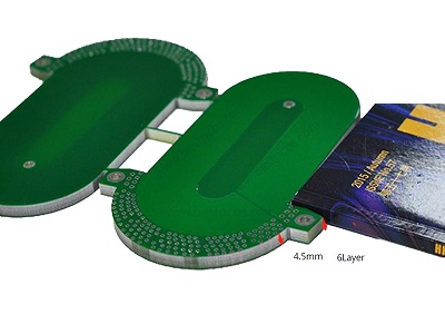
What is the Thickness of Copper in Heavy Copper PCB?
Heavy copper PCBs feature copper thickness from 3 oz (0.105 mm) to 15 oz (0.525 mm). These boards are used in high-current and rugged environments, including military, automotive, and industrial applications. Such boards withstand stress and high temperatures better.
| Specification | Details |
|---|---|
| Base Material | FR4 / Aluminum |
| Copper Thickness | 4 OZ ~ 10 OZ |
| Extreme Heavy Copper | 20 OZ ~ 200 OZ |
| Outline | Routing, Punching, V-Cut |
| Soldermask Colors | White, Black, Blue, Green, Red Oil |
| Surface Finishing | Immersion Gold, HASL, OSP |
| Max Panel Size | 580 × 480 mm (22.8\” × 18.9\”) |
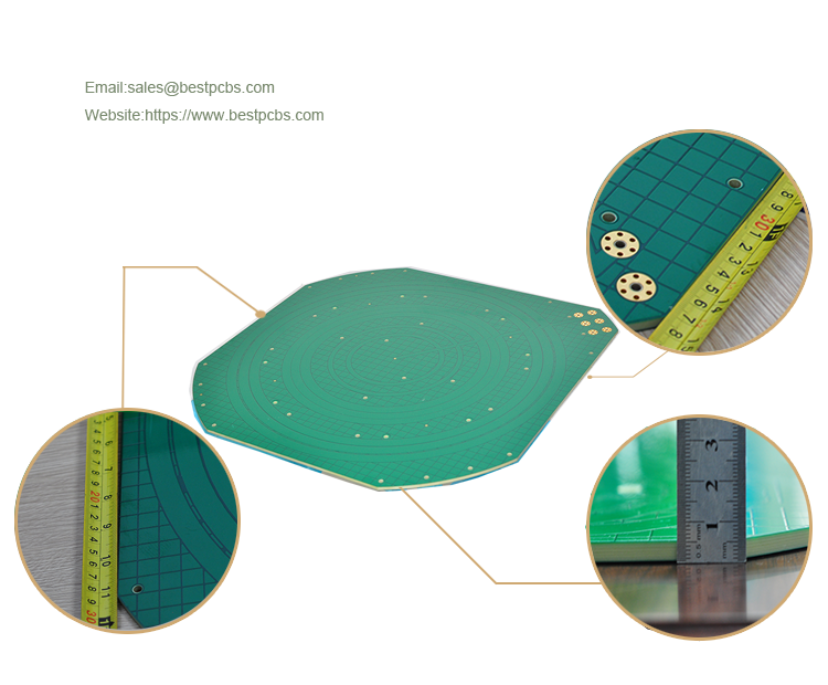
How to Measure Copper Thickness on PCB?
Copper thickness can be measured by cross-section analysis or X-ray fluorescence (XRF). These methods provide precise results, especially when verifying custom or plated copper layers. Many PCB manufacturers provide a PCB copper thickness chart for quick reference.
How to Choose PCB Copper Thickness on PCB?
When selecting copper thickness, consider these points:
- Current load – higher current needs thicker copper.
- Thermal management – thicker copper helps spread heat.
- Board size – small boards with high current must compensate with thickness.
- Cost – more copper means higher cost.
All in all, use a copper thickness on PCB calculator to match your design needs accurately.
Why Choose EBest Circuit (Best Technology) for Custom Copper Thickness on PCB Service?
Customers often face delays, inconsistent quality, or limited customization. At EBest Circuit (Best Technology), we understand these pain points. Our services offer:
- Full Customization: From 0.5 oz to 15 oz copper, tailored to your project needs.
- Precision and Quality: Advanced equipment ensures consistent plating and copper thickness.
- Fast Turnaround: Quick prototyping and reliable mass production, reducing your time to market.
- Certifications: ISO9001, AS9100D, ISO13485, IATF16949, UL, RoHS – giving you high quality PCBs.
- 24/7 Technical Support: Experienced engineers provide advice on copper thickness for your design goals.
Above are EBest Circuit (Best Technology)’s distinctive traits. You’ll know exactly what’s on your board and how it performs. No guesswork, no delays. We will give the optimal solution that works for you, and your project will move forward with ease.
To sum up, copper thickness on PCB affects everything from current flow to thermal stability. Whether you need standard or heavy copper, getting it right improves reliability and performance. EBest Circuit (Best Technology) not only helps you select the right thickness but also ensures top-quality results, every time. By solving common challenges such as slow delivery, lack of expertise, and inconsistent results, we support your PCB success from prototypes to full assembly. Reach out to us at sales@bestpcbs.com, then get a quote or discuss your design together.