

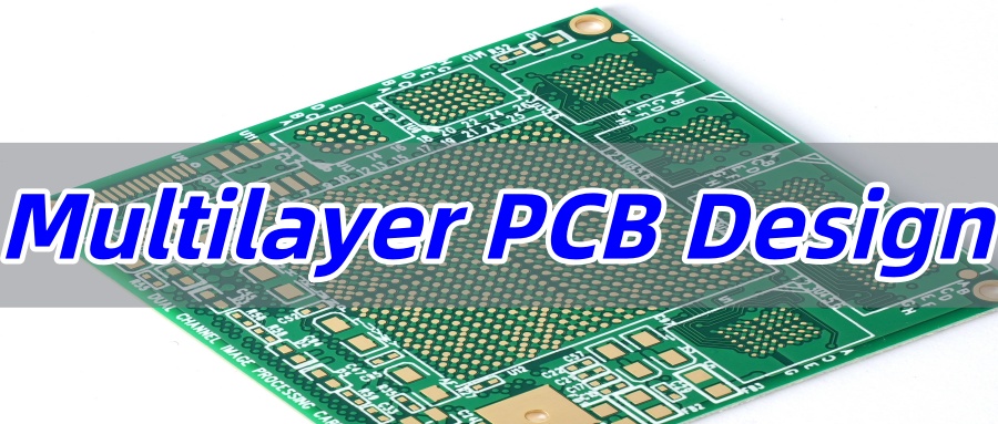
Multilayer PCB design is the engineering process of creating printed circuit boards with three or more conductive copper layers, which is essential for packing complex functionality into today’s compact, high-performance electronic devices. This article provides a comprehensive guide to multilayer PCB design principles, best practices, and how to find reliable expert solutions for your projects.
What are the Common Pain Points in Multilayer PCB Design?
- Signal Integrity Issues: Managing crosstalk, EMI, and impedance in high-speed or multilayer RF PCB design becomes extremely difficult as complexity increases.
- Complex Stack-up Configuration: Choosing the right materials, layer count, and sequence (a core multilayer PCB design consideration) without expert knowledge can lead to poor performance or high costs.
- Manufacturing Headaches: Designs that ignore multilayer PCB design for assembly guidelines or capabilities result in low yields, delays, and unexpected expenses.
- Inefficient Thermal Management: Failure to properly plan for heat dissipation in dense multilayer circuit boards can cause overheating and premature device failure.
- Tool Limitations: Using basic software that lacks advanced PCB tools multilayer design support for HDI (High-Density Interconnect) features can severely limit your design possibilities.
Fortunately, these challenges can be effectively mitigated by partnering with an experienced provider. The solution lies in accessing a combination of expert knowledge and advanced capabilities.
Core Solutions for Successful Multilayer PCB Design:
- Expert Layout for Signal Integrity: Our engineers employ proven multilayer PCB design techniques and strict multilayer PCB design rules to ensure clean signals and robust EMC performance.
- Optimized Stack-up Planning: We provide expert guidance on the multilayer PCB design process, including material selection and layer stack-up, to balance performance, reliability, and cost-effectiveness.
- DFM/DFA-Optimized Designs: Our multilayer PCB design services are built around multilayer PCB design for assembly guidelines, ensuring your board is easy to manufacture and assemble, saving time and money.
- Integrated Thermal Analysis: We implement strategic multilayer PCB design tips like thermal vias and plane partitioning to manage heat effectively from the initial design stages.
- Advanced Design Tool Proficiency: Our team uses state-of-the-art multilayer PCB design software like Altium Designer, which offers comprehensive multilayer PCB design support for even the most complex HDI projects.
At BEST Technology, we are a professional PCB manufacturer and design service provider with deep expertise in delivering robust, high-yield multilayer solutions. Our engineering team leverages advanced tools and proven multilayer PCB design guidelines to turn complex concepts into manufacturable reality, ensuring reliability from prototype to SMT PCBA assembly. For a multilayer printed circuit consultation, pls feel free to contact us at sales@bestpcbs.com.
What Is Multilayer PCB Design and Why It Matters in Modern Electronics?
Multilayer PCB design involves arranging electrical circuits on multiple layers of insulating substrate, interconnected by plated through-holes or microvias. This introduction will explain its fundamental importance.
- Increased Circuit Density: The primary advantage is the ability to host more components and complex wiring in a smaller area, which is crucial for smartphones, wearables, and advanced computing systems.
- Enhanced Performance: Dedicated power and ground planes improve power integrity, reduce EMI, and allow for controlled impedance routing, which is vital for high-speed digital and multilayer RF PCB design.
- Improved Reliability: A well-planned multilayer board is generally more robust than a double-sided board, with better resistance to environmental factors and physical stress due to a more balanced structure.
In summary, multilayer PCB designing is not just an option but a necessity for modern electronics, enabling the advanced features and miniaturization that consumers demand. Partnering with an expert is key to unlocking these benefits.
How to Design Multilayer PCB?
The multilayer PCB design process is a structured sequence of critical steps that balances electrical performance, manufacturability, and cost. Following a proven methodology, as detailed in expert resources, is the difference between success and failure. This process involves strategic planning from layer stack-up to final validation.
1. Define Requirements and Schematic Capture
Start by finalizing the schematic and defining system requirements. This foundational stage directly influences all subsequent decisions.
- Determine Board Specifications: Analyze the circuit’s scale, board size, and critical performance requirements, especially Electromagnetic Compatibility (EMC).
- Assess Wiring Density: Use EDA tools after component pre-layout to analyze potential routing bottlenecks. This assessment helps in estimating the necessary number of signal layers.
- Identify Critical Signals: Classify special signals such as high-speed lines, differential pairs, and sensitive analog lines. Their quantity and requirements are key factors in deciding the layer count and stack-up strategy.
2. Plan the Layer Stack-up
This is a foundational step where the PCB’s performance is largely determined. The goal is to determine the number of layers, their function (signal, power, ground), sequence, and material thickness.
- Determine Layer Count: Balance routing needs against cost and manufacturing complexity. The number of power domains and grounding requirements will determine the number of internal planes.
- Adhere to Key Stack-up Principles:
- Shielding: Each signal layer should be adjacent to an internal power or ground plane (e.g., Top-Layer next to GND plane) to use the copper layer as a shield.
- Power-Ground Coupling: The core internal power and ground layers should be tightly coupled by using a thin dielectric thickness between them. This improves decoupling and increases resonant frequency.
- High-Speed Signal Isolation: High-speed signal layers should be embedded between two internal planes (e.g., Signal layer between GND and POWER), which confines EMI and provides shielding.
- Avoid Adjacent Signal Layers: Prevent two signal layers from being directly adjacent to minimize crosstalk. If unavoidable, add a ground plane between them.
- Symmetry: Maintain a symmetrical layer stack-up to prevent board warping during manufacturing.
- Select an Optimal Configuration: Based on the principles above, choose a standard stack-up. For example, a preferred 4-layer stack is: Top (Signal) -> GND (Inner 1) -> POWER (Inner 2) -> Bottom (Signal). A preferred 6-layer stack is: Top (Signal) -> GND (Inner 1) -> Signal (Inner 2) -> POWER (Inner 3) -> GND (Inner 4) -> Bottom (Signal). These configurations provide excellent shielding and tight power-ground coupling. The stack-up is defined using the EDA software’s Layer Stack Manager.
3. Component Placement with DFM and Modularity
Place critical components first, considering signal flow, thermal management, and most importantly, Design for Manufacturability (DFM).
- Modular by Power Domain: Group components that share the same power supply and ground type together. This simplifies the later task of internal plane segmentation.
- Prioritize Interface and High-Noise Components: Place connectors on the board edges for easy access. Position noisy components (e.g., clock generators, switching regulators) close to their target components (like a CPU) but away from sensitive analog circuits.
- Consider Manufacturing: Prefer single-sided component placement. If double-sided, place only surface-mount devices (SMDs) on the bottom layer. Ensure adequate spacing for automated assembly and soldering.
- Implement Decoupling: Place decoupling capacitors (e.g., 0.1µF) close to the power pins of ICs. Larger filter capacitors (e.g., 10µF) should be placed near power entry points.
4. Routing and Critical Net Prioritization
Route signals based on priority, adhering to strict rules for spacing and impedance.
- Route by Priority: Route high-speed clocks, differential pairs, and sensitive analog signals first, ensuring they have continuous reference planes and meet impedance constraints.
- Follow General Routing Rules:
- Trace Width: Calculate width based on current. A general rule is 1A per 1mm of trace width (for 0.05mm copper thickness). Power and ground traces should be wider (≥50mil).
- Spacing: Maintain sufficient clearance between traces, especially for high-voltage differences. A common rule is 5.08V/mil for electrical insulation.
- Corners: Use 45-degree angles or arcs instead of 90-degree sharp corners to avoid RF radiation and manufacturing issues.
- Shielding: For critical high-frequency signals, use a “guard trace” – a grounded trace that runs alongside the signal to isolate it.
- Separate Analog and Digital Grounds: Keep analog and digital grounds separate, connecting them only at a single point to prevent ground loops.
- Plan for Internal Planes: Route all signal lines first. The power and ground connections will be completed through the internal planes using vias.
5. Internal Plane Design and Segmentation
For boards with multiple power domains, the internal power plane must be segmented into isolated regions.
- Use the Split Plane Tool: In your EDA software (e.g., Altium’s Split Planes tool), define polygonal boundaries for each power net on the internal plane.
- Set Clearance Rules: Define rules for Power Plane Clearance (insulation gap around non-connected vias) and Power Plane Connect Style (thermal relief connection for pins).
- Key Considerations: Ensure the segmentation boundary does not pass over a pad that belongs to the same net, as this can cause connection issues.
6. Design Rule Check (DRC) and Final Validation
The final step is a comprehensive verification against a set of rules to ensure the design is error-free and manufacturable.
- Run a Comprehensive DRC: Check against your manufacturer’s capabilities for trace width, spacing, hole sizes, and other physical constraints.
- Validate Plane Connections: Ensure all power and ground pins are correctly connected to their respective planes with the appropriate style (e.g., thermal relief).
- Add Final Touches: Perform teardroping (adding tapered transitions between pads and tracks) to improve mechanical strength. Add copper pours on unused areas of signal layers and connect them to ground to shield noise.
- Final Review: Check for consistency in silkscreen labels, component orientation, and that no critical guidelines have been violated.
Ultimately, knowing how to design multilayer PCB effectively requires a disciplined approach that balances sophisticated electrical principles with practical physical manufacturability. By meticulously following these steps—from strategic stack-up planning governed by multilayer PCB design guidelines to rigorous final validation—you can transform a complex schematic into a reliable, high-performance multilayer circuit board. If you would like to send us any inquiry about 2 layer printed circuit board, 4 layer PCB, 6 layer PCB stack, 8 layer PCB stackup or any other PCB board layers, please send us an email through the contact form at the bottom of our Contact Page.
How Do Advanced PCB Tools Support Multilayer and HDI Designs?
Modern multilayer PCB design software is equipped with specialized features that are indispensable for complex designs. Advanced PCB tools multilayer design support is a critical enabler for HDI.
- Integrated 3D Modeling: Tools like Altium Designer allow designers to check for mechanical clearances in real-time, preventing conflicts with enclosures in dense multilayer PCB board design.
- Automated HDI Feature Generation: They support the creation of microvias, via-in-pad, and stacked/stitched vias automatically, which are essential for breaking out high-pin-count BGAs in HDI designs.
- Sophisticated Simulation: Built-in signal and power integrity analysis help predict and solve problems like reflections and simultaneous switching noise (SSN) before the board is fabricated.
- Dynamic Stack-up Management: These tools provide a visual interface for defining and modifying the layer stack-up, including materials and dielectric constants, which directly feed into impedance calculators.
In conclusion, how do advanced PCB tools support multilayer and hdi designs? They provide an integrated environment that automates complex tasks, enforces design rules, and provides analytical capabilities that are impossible to replicate manually, ensuring a higher chance of first-pass success.
How Do Multilayer RF PCB Design Principles Improve High-Frequency Applications?
Multilayer RF PCB design is a specialized discipline critical for the success of high-frequency applications in wireless communication, radar systems, and advanced networking. By adhering to strict design principles, manufacturers like EBest Circuit (Best Technology) can overcome the inherent challenges of high-frequency signals, such as signal loss, interference, and integrity degradation. These principles leverage the multilayer structure to achieve superior performance, reliability, and miniaturization.
Controlled Impedance and Signal Integrity Management
- A. Precise Trace Geometry and Dielectric Control:
- Multilayer stack-ups allow for the use of calculated dielectric core and prepreg thicknesses to create controlled impedance transmission lines (e.g., 50Ω or 75Ω). This is essential for minimizing signal reflections and ensuring power is efficiently transferred.
- The capability to maintain tight impedance tolerances (e.g., ±10% for values >50 ohm, ±5 ohm for values ≤50 ohm) is a direct result of sophisticated design and manufacturing control.
- B. Minimized Crosstalk and EMI:
- By dedicating entire layers within the multilayer stack-up as ground or power planes, RF signals can be effectively shielded. These solid planes act as reference planes and contain electromagnetic fields, reducing crosstalk between adjacent signals and minimizing electromagnetic interference (EMI).
Advanced Material Utilization for Optimal Performance
- A. Selection of Low-Loss High-Frequency Laminates:
- RF-specific materials like Rogers (RO4003, RO4350), Taconic, and Isola FR408HR are used in critical signal layers. These materials have a stable dielectric constant (Dk) and a very low dissipation factor (Df), which significantly reduces signal loss at high frequencies.
- The multilayer approach allows for the strategic (and cost-effective) use of these expensive high-frequency materials only where needed, combined with standard FR4 for other layers.
- B. Enhanced Thermal Management:
- High-frequency circuits can generate significant heat. Multilayer designs facilitate efficient thermal dissipation by incorporating thermal vias that transfer heat from inner layers or components to external heatsinks or dedicated metal core layers, such as those used in Metal Core PCBs (MCPCBs).
Improved Shielding and Grounding Techniques
- A. Robust Ground Plane Implementation:
- A fundamental principle is providing an uninterrupted, low-impedance ground path. Multilayer PCBs enable the use of dedicated ground planes adjacent to RF signal layers, creating a consistent return path and shielding the signal from noise.
- B. Shielding Cavities and Via Fencing:
- “Via fencing”—rows of grounded vias placed along the edges of an RF transmission line—creates a shielding cavity that prevents radiation and isolates the RF section from other digital or analog parts of the circuit, a technique perfectly suited for multilayer boards.
Miniaturization and Integration Capabilities
- A. Complex Circuitry in a Compact Form Factor:
- Multilayer construction allows for a high density of interconnections within a small footprint. This is crucial for modern devices where space is limited, enabling the integration of RF front-end modules, amplifiers, and antennas into a single, compact package.
- B. Support for HDI and Microvia Technology:
- For very high-frequency designs, HDI principles with microvias (as small as 4mil/0.1mm) are employed to facilitate dense component placement and shorter signal paths, which is essential for minimizing parasitic effects and propagation delay at high frequencies. The use of advanced PCB machine like laser drill machines is critical for this capability.
Enhanced Manufacturing Precision and Quality Assurance
- A. Strict Tolerances for High-Frequency Features:
- RF designs require extreme precision in feature sizes. Manufacturing capabilities such as tight trace width/space tolerance (e.g., ±1mil for special processes), controlled dielectric thickness, and precise plating are non-negotiable.
- B. Comprehensive Testing and Validation:
- Ensuring the performance of an RF PCB necessitates rigorous testing. Manufacturers equipped with Automated Optical Inspection (AOI) for layer alignment, X-Ray copper thickness testers, and network analyzers for impedance and S-parameter verification are essential to validate that the built board matches the design intent.
In summary, multilayer RF PCB design principles are foundational to advancing high-frequency applications. By enabling controlled impedance, superior signal integrity, effective shielding, and significant miniaturization, these principles directly address the core challenges of high-speed circuits. Partnering with a manufacturer that masters these principles—from material selection and sophisticated design to precision manufacturing and rigorous testing—ensures that high-frequency products meet their demanding performance, reliability, and size requirements.
How to Optimize Multilayer PCB Design for Assembly Guidelines and Manufacturing Efficiency?
Designing for manufacturability (DFM) and assembly (DFA) is critical for cost control and yield. Adhering to multilayer PCB design for assembly guidelines bridges the gap between a working design and a profitable product.
- Component Selection and Placement: Choose standard, readily available components. Place them with sufficient spacing for automated pick-and-place machines and soldering nozzles. Avoid placing tall components too close to each other.
- Solderability and Thermal Relief: Use thermal relief connections for pins connected to large power or ground planes to prevent solder defects during wave soldering. Ensure pad sizes are appropriate for the soldering process.
- Fiducial Marks and Tooling Holes: Include global and local fiducial marks to assist automated assembly equipment with accurate board alignment. Add tooling holes for secure fixture during assembly.
- Clear Silkscreen and Polarity Marking: Provide a clear, non-overlapping silkscreen layer for component designators and polarity indicators. This is vital for both automated assembly and future troubleshooting.
By integrating these multilayer PCB design for assembly guidelines early in the multilayer PCB design process, you significantly reduce the risk of errors, speed up production, and lower overall costs, making your product more competitive.
What Are the Benefits of Using Multilayer Flex PCB Design in Compact Electronics?
The drive for smaller, lighter, and more powerful electronic devices has made Multilayer Flex PCBs (Rigid-Flex) a critical enabling technology. For a company like EBest Circuit (Best Technology), which specializes in advanced PCB solutions, leveraging multilayer flex design offers significant advantages in compact electronic applications.
Superior Space Efficiency and Miniaturization
- A. Three-Dimensional Configuration:
- Unlike traditional rigid boards, flex circuits can be bent, folded, and twisted to fit into uniquely shaped and confined spaces, allowing for optimal use of the device’s internal volume.
- This 3D packaging capability is essential for modern compact electronics like smartphones, wearables, and medical implants.
- B. Reduction in Connectors and Cables:
- Multilayer flex designs can integrate multiple interconnections into a single, continuous unit, eliminating the need for bulky connectors, wiring harnesses, and solder joints.
- This reduction in components directly translates to space and weight savings, increased reliability, and a simpler assembly process.
Enhanced Reliability and Durability
- A. Reduced Failure Points:
- By creating a single, interconnected unit, rigid-flex boards minimize the number of plug-in connections, which are common points of failure due to shock, vibration, or corrosion.
- B. High Mechanical Stability:
- Flex materials like polyimide can withstand millions of dynamic flexing cycles, making them ideal for applications with moving parts or repeated use.
- The integration of rigid sections provides stability for mounting components, while the flexible sections absorb stress and vibration.
Advanced Design Capabilities for Complex Applications
- A. High-Density Interconnect (HDI) Support:
- Multilayer flex PCBs are compatible with HDI technologies, such as microvias (as small as 4mil/0.1mm), allowing for a higher number of interconnections in a smaller area. This is crucial for complex, high-pin-count components like BGAs.
- B. Impedance Control and Signal Integrity:
- The controlled dielectric properties of flex materials allow for precise impedance matching, which is vital for high-speed and high-frequency signals, reducing crosstalk and ensuring data integrity in advanced electronics.
- C. Material Versatility:
- Manufacturers like EBest Circuit (Best Technology) can combine standard FR4, high-frequency materials (Rogers, Taconic), and flexible substrates to meet specific electrical, thermal, and mechanical requirements within a single assembly.
Streamlined Assembly and Supply Chain (Turnkey Solution)
- A. Simplified Assembly Process:
- A single, integrated rigid-flex board is easier to handle and install than multiple interconnected rigid boards, reducing assembly time, labor costs, and potential for human error.
- B. Full Turnkey Service Advantage:
- Partnering with an expert manufacturer that offers end-to-end services—from design and fabrication to component sourcing and assembly—ensures a seamless process. This “one-stop” approach, as highlighted by EBest Circuit (Best Technology), improves communication efficiency and shortens overall lead times.
High-Quality and Rapid Prototyping for Faster Time-to-Market
- A. Guaranteed Quality through Rigorous Testing:
- Specialized manufacturers employ strict quality control procedures, including Automated Optical Inspection (AOI) and Flying Probe Testing, to ensure the reliability of complex multilayer flex prototypes and production runs. This is backed by certifications like ISO 9001 and IATF 16949.
- B. Accelerated Development Cycles:
- The ability to rapidly prototype multilayer flex designs (e.g., lead times as fast as 1.5 weeks for 4-layer rigid-flex) allows for quick design validation and iteration, significantly reducing the product development cycle and enabling a faster time-to-market.
In summary, the use of multilayer flex PCB design is not just a manufacturing choice but a strategic enabler for innovation in compact electronics. The benefits of unmatched space savings, superior reliability, and advanced electrical performance—supported by the expertise and turnkey services of a specialized manufacturer—make it an indispensable solution for creating the next generation of smaller, smarter, and more reliable electronic devices.
What Are the PCB Design Capabilities Multilayers Companies Must Offer to Support Complex Electronics?
When selecting a partner for complex electronics, it’s crucial to choose a manufacturer whose design capabilities match the technical demands of your project. With our extensive experience, we position ourselves as a full-turnkey partner, offering a suite of advanced design services that go beyond simple board layout. Here’s how our capabilities align with the key requirements for supporting sophisticated multilayer designs.
1. Signal and Power Integrity (SI/PI) Analysis
While manufacturing precision is the foundation of good SI/PI performance, our capabilities reflect a strong understanding of these principles. Our expertise in manufacturing boards with controlled impedance is a direct indicator.
- Real-World Capability: We explicitly offer impedance control with tight tolerances: ±10% for values >50 ohm and ±5 ohm for values ≤50 ohm. This is critical for high-speed digital and RF circuits to prevent signal degradation.
- Material Expertise: Our experience with a wide range of materials, including high-frequency boards (Rogers, Taconic), is essential for SI engineers to select substrates with appropriate dielectric constants and loss tangents for the application.
- Manufacturing Precision: Our advanced equipment, such as the X-Ray Copper Thickness Tester from Germany, ensures consistent copper thickness, a key factor in achieving predictable impedance and power delivery network (PDN) performance.
2. EMI/EMC Design and Mitigation
Our focus on quality and certifications demonstrates our commitment to producing reliable, compliant products. Our experience with specific board types is crucial for EMI/EMC design.
- Design for Manufacturing (DFM): As part of our turnkey service, we provide DFM checks, which inherently include reviewing designs for potential EMI issues, such as improper return paths or insufficient shielding, and correcting them before production.
- Material Solutions: We are proficient in producing Metal Core PCBs (MCPCBs), which is a significant advantage for thermal management and EMI shielding in high-power applications like LED lighting and power supplies.
- Certification Framework: Holding certifications like ISO 9001, ISO 13485, IATF 16949, AS9100D proves that our systems are designed to meet the stringent reliability and EMC standards required.
3. HDI and Microvia Expertise
Our technical specifications clearly showcase our advanced manufacturing capabilities, which are essential for implementing HDI designs.
- Microvia Drilling: Our CNC Laser Drill Machine enables the creation of microvias as small as 4 mil (0.1mm), facilitating high-density interconnections between layers.
- Fine Line Technology: We offer min trace width/space of 2/2 mil for HDI designs on FR4 PCBs, allowing more routing channels in a smaller area—essential for complex, miniaturized multilayer boards in smartphones, wearables, and advanced networking equipment.
- High Layer Count: We can manufacture up to 32-layer FR4 PCBs, demonstrating our capability to manage complex, high-density interconnects (HDI) and sophisticated stack-ups common in servers and communication hardware.
4. Flex/Rigid-Flex PCB Design
This is a standout area for us. We specialize in flexible circuits, making us a strong partner for products requiring durability and 3D packaging.
- Comprehensive Flex Design Service: We offer both OEM and ODM flexible circuit board design. For ODM projects, we create custom designs based on application parameters, impedance, current, and bending requirements, which is critical for dynamic flex applications.
- Advanced Manufacturing: We can produce complex structures like multilayer flex circuits (up to 10 layers) and rigid-flex boards. A recent collaboration with a German solar manufacturer for 200,000 pieces of multi-layer rigid-flex PCBs demonstrates our capacity for large-scale, complex projects.
- Design Validation: We utilize 3D PCB model displays to check for structural and design defects in flex and rigid-flex designs before prototyping, reducing the risk of failure and ensuring the board fits and functions within the intended product enclosure.
In closing, we demonstrate a clear commitment to supporting complex electronics through our advanced multilayer PCB design and manufacturing capabilities. By offering a full turnkey service that integrates PCB design, DFM, prototyping, and assembly, we ensure that design intent is faithfully translated into a high-quality, reliable product. Our specific expertise in impedance control, HDI technology, and flex/rigid-flex multilayer circuit board solutions, backed by relevant certifications and state-of-the-art equipment, makes us a capable partner for industries ranging from automotive and medical to consumer electronics and renewable energy.
Why Partner with a China Multilayer PCB Design Expert for Reliable Production?
Partnering with an expert PCB manufacturer in China, particularly one with deep specialization in multilayer design and production, offers a strategic advantage for businesses seeking reliability, innovation, and cost-effectiveness. Companies like EBest Circuit (Best Technology) exemplify this by combining 19 years of experience with comprehensive, vertically integrated services.
Unmatched Technical Expertise and Specialized Knowledge
- A. Deep Industry Experience:
- Proven track record (e.g., EBest Circuit (Best Technology) has over 19 years since 2006) in handling complex PCB projects.
- Long-term evolution with industry trends, ensuring knowledge of both foundational and cutting-edge techniques.
- B. Specialization in Advanced Multilayer PCBs:
- Capability to produce high-layer-count boards (e.g., up to 32 layers for FR4 PCBs) and manage their inherent complexities, such as impedance control and signal integrity.
- Experience with diverse and challenging materials beyond standard FR4, including:
- Metal Core PCBs (MCPCBs): For superior thermal management (e.g., thermal conductivity up to 3.0 W/m.K).
- Ceramic PCBs: For high-temperature and high-frequency applications.
- Special PCBs: Expertise in Heavy Copper (up to 20 OZ), HDI, and Rigid-Flex boards.
- C. Design for Manufacturing (DFM) Support:
- Expert engineers provide DFM analysis early in the design phase to identify and rectify potential production issues, significantly increasing final product yield and reliability.
- This proactive approach prevents costly redesigns and delays, ensuring the design is optimized for manufacturability.
Rigorous Quality Assurance and Certifications
- A. Certified Quality Management Systems:
- Adherence to international standards validated by certifications such as ISO9001:2015, IATF16949, and ISO13485:2016, which guarantee consistent and controlled processes.
- Compliance with RoHS and REACH ensures environmental responsibility and material safety.
- B. Comprehensive In-House Testing and Inspection:
- Investment in state-of-the-art equipment for rigorous quality control at every production stage.
- Capabilities include:
- Automated Optical Inspection (AOI): For defect detection.
- Flying Probe & Universal E-Testing: For accurate electrical verification of open/short circuits.
- X-Ray Copper Thickness Testers and Micro-Section Analysis: For precise measurement and internal structure verification.
- A commitment to high-quality standards, with a documented on-time delivery rate of 97% and strict adherence to IPC standards.
Cost-Effectiveness Without Compromising Reliability
- A. Economies of Scale and Optimized Processes:
- Large-scale production capabilities (e.g., 28,900 sq. meter monthly capacity) and efficient supply chain management lead to significantly lower unit costs.
- B. “No MOQ” (Minimum Order Quantity) Flexibility:
- Accommodates both prototype development and mass production, allowing clients to order small batches for testing without financial penalty, de-risking the introduction of new products.
Full Turnkey Solution: Simplifying the Supply Chain
- A. End-to-End Service Integration:
- A single point of contact for the entire process, from PCB design and layout to component sourcing, PCB assembly, and final box build.
- This eliminates the complexity and communication gaps of managing multiple vendors, reducing lead times and improving accountability.
- B. One-on-One Expert Support:
- Dedicated engineering sales and support teams provide personalized communication and problem-solving throughout the project lifecycle.
Advanced Manufacturing Capabilities and Rapid Prototyping
- A. State-of-the-Art Equipment:
- Utilization of advanced machinery from global leaders (e.g., Hitachi, Posalux) for drilling, plating, and inspection, ensuring high precision and repeatability.
- B. Accelerated Development Cycles:
In brief, EBest Circuit (Best Technology) provides access to deep technical expertise, guaranteed quality through certified processes, significant cost savings, and a simplified, integrated production model. This partnership ultimately de-risks production, accelerates innovation, and ensures the reliable delivery of high-performance electronic products in a competitive global market.
Overall, multilayer PCB design is a sophisticated engineering discipline that underpins the functionality of modern electronics, requiring a deep understanding of electrical principles, materials, and manufacturing processes. This article has explored the key aspects of designing multilayer PCBs, from fundamental steps to advanced considerations for HDI and RF applications. For projects where performance, reliability, and time-to-market are critical, partnering with an expert is the most effective path to success. BEST Technology offers comprehensive multilayer PCB design services, combining engineering expertise with advanced manufacturing capabilities to deliver robust, high-performance solutions. For expert assistance with your next multilayer PCB project, please contact us at sales@bestpcbs.com.