

An HDMI digital modulator is a critical device that converts high-definition multimedia interface (HDMI) signals into broadcast-standard RF signals for distribution over coaxial cable networks. This article delves into the core PCB design and PCBA manufacturing challenges and services required to build reliable digital HDMI modulators.
Developing a high-performance HDMI modulator often exposes design teams to a set of tightly coupled PCB and PCBA challenges.
- Extremely Complex PCB Layout
High-speed HDMI, digital processing, and RF circuitry must coexist on dense multi-layer boards. - Severe Signal Interference
Crosstalk, EMI, and noisy power rails degrade RF modulation quality. - Thermal Management Issues
Heat from FPGAs, encoders, and RF stages impacts stability and lifetime. - Component Sourcing & Assembly Risks
Fine-pitch BGAs, RF shielding, and long-lifecycle IC availability increase build difficulty. - Inconsistent Yield and Performance
PCB impedance variation and SMT process drift reduce production yield.
Addressing these risks requires a PCB and PCBA partner with proven experience in high-speed and RF-integrated designs.
- Advanced Multi-Layer PCB Design
8+ layer stack-ups with controlled impedance and clear digital/RF partitioning. - Signal and Power Integrity Control
Pre-layout and post-layout analysis to suppress EMI and crosstalk. - Thermal and Reliability Engineering
Optimized materials, thermal vias, and heat dissipation strategies. - DFM-Driven Component Procurement
Verified sourcing combined with assembly-focused design optimization. - Targeted Functional and RF Testing
ICT, RF signal validation, and thermal stress testing for each HDMI digital RF modulator.
At EBest Circuit (Best Technology), we are a specialized PCB fabrication and turnkey PCBA assembly manufacturer focused on complex, high-frequency, and mixed-signal PCB and PCBA products like modulators. Our core advantage lies in comprehensive DFM analysis and BOM optimization, supported by R&D, PCB, and PCBA engineers with over 20 years of hands-on experience, who provide practical manufacturing-focused recommendations to ensure your HDMI digital modulator PCB or SMT design is optimized for reliable mass production. Contact us at sales@bestpcbs.com to transform your design into a robust product.
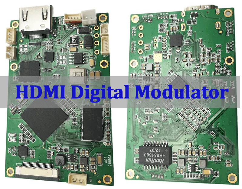
What Is an HDMI Digital Modulator From a PCB and PCBA Perspective?
From a PCB and PCBA standpoint, an HDMI digital modulator is a convergence of several high-performance electronic subsystems on a single, complex printed circuit board. Its core function—encoding and modulating an HDMI stream into an RF signal—dictates a challenging integration of diverse technologies.
- High-Speed Digital Interface: The HDMI input stage requires a multi-gigabit serial link, demanding controlled impedance routing (typically 100Ω differential) and strict length matching on the PCB.
- Digital Processing Core: An FPGA or dedicated encoder chip performs video compression (e.g., MPEG-2/H.264) and multiplexing. This area requires dense BGA fanouts, clean power planes, and often external DDR memory.
- RF Modulation & Upconversion: This is the heart of the digital HDMI to RF modulator. A DAC and mixer translate the digital stream to an intermediate frequency (IF), which is then upconverted to the target RF channel (e.g., QAM, ATSC, DVB-T). PCB layout here is critical to avoid noise injection.
- Power Management Network: Multiple, isolated voltage rails (e.g., 1.0V, 1.8V, 3.3V, 5V) with low noise are needed for different ICs. This involves switch-mode regulators and LDOs, placed to minimize switching noise interference.
- Output Conditioning & Protection: The final RF signal passes through amplifiers, SAW filters, and protection circuits before reaching the F-connector. Transmission line integrity up to the connector is paramount.
In essence, the PCB for an HDMI digital encoder modulator is a carefully orchestrated platform where digital signal integrity, RF purity, and thermal management must coexist. The PCBA process must then accurately populate and solder this sophisticated board.
How a Digital HDMI Modulator Is Implemented on a Multi-Layer PCB?
Implementing a digital HDMI modulator requires a carefully planned multi-layer PCB architecture to manage high-speed signal routing, power integrity, RF isolation, and thermal performance. In practice, an 8–12 layer stack-up is commonly used to separate functional domains and ensure stable operation.
Typical Multi-Layer PCB Stack-Up Overview
| Layer | Primary Function | Key Considerations |
|---|---|---|
| L1 (Top) | Components, HDMI & RF signals | Controlled-impedance routing |
| L2 | Solid ground plane | Clean return path, shielding |
| L3 | Digital signal routing | Control and logic signals |
| L4 | Power plane (Core voltage 1) | Noise-sensitive digital power |
| L5 | Power plane (RF / analog) | Isolated RF power regions |
| L6 | Internal digital signals | FPGA / encoder switching |
| L7 | Solid ground plane | Reference for bottom signals |
| L8 (Bottom) | Power & large components | Regulators, bulk passives |
The stack-up structure prioritizes signal reference integrity, power isolation, and RF containment rather than routing density alone.
Functional Partitioning of the PCB
Partitioning is critical in HDMI digital modulator designs. The PCB is divided into clearly defined zones:
- HDMI input and TMDS processing
- Digital processing (FPGA / encoder)
- RF synthesis and modulation
- RF output and matching network
Physical separation between these zones minimizes coupling between noisy digital sections and sensitive RF circuitry.
RF Shielding and Grounding Strategy
Sensitive RF blocks such as VCOs, mixers, and output drivers are protected using:
- Grounded copper pour fences on the top layer
- Dense via stitching tying fences to internal ground planes
- Short, low-inductance ground connections
This approach effectively creates localized Faraday cages that suppress EMI and prevent digital noise from contaminating the RF spectrum.
Via Structure and Thermal Management
A combination of via types is required to support both signal escape and thermal control:
- Through vias for general connectivity
- Blind and buried vias for dense BGA fan-out
- Thermal vias under FPGAs, encoders, and RF amplifiers
Thermal vias conduct heat into internal planes or toward bottom-side heatsinks, improving long-term reliability and frequency stability.
It is clear that this structured, multi-layer PCB methodology is essential for building a stable and manufacturable HDMI digital RF coaxial modulator. It allows HDMI processing, digital control, and RF modulation subsystems to operate concurrently without mutual interference, while maintaining consistent performance across production volumes.
Key PCB Design Challenges in an HDMI Digital RF Modulator
Designing the PCB for an HDMI digital RF modulator presents a unique set of challenges where digital and RF design disciplines collide. Success hinges on anticipating and mitigating these issues from the first layout.
- Mixed-Signal Coexistence & Isolation: The primary challenge is isolating the noisy digital domain (FPGA, switching regulators) from the sensitive RF analog domain. This requires careful floor planning, the use of separate ground planes that are tied together at a single point (often near the power input), and strategic placement of moats (splits in power planes).
- Impedance Control Across the Board: Different signals have different requirements:
- HDMI: 100Ω differential pairs.
- RF Traces: 50Ω single-ended (e.g., from mixer to amplifier).
- DDR Memory: Specific single-ended impedance (e.g., 40Ω). The PCB stack-up must be calculated to achieve these impedances simultaneously across different layers and trace widths.
- Thermal Management at the PCB Level: High-power components (FPGA, RF PA) concentrate heat. The PCB itself must act as a heat spreader. This involves using thick copper planes (2oz+), arrays of thermal vias under components, and designing keep-out areas under thermally sensitive parts like crystal oscillators.
- Power Integrity (PI) Design: The digital core can draw current in large, fast bursts, causing voltage droop. A robust PI network involves using multiple decoupling capacitors of different values (bulk, ceramic) placed very close to IC power pins, and ensuring low-impedance power delivery networks (PDNs) through wide planes and short connections.
- Material Selection for RF Performance: While FR-4 is sufficient for digital sections, the final RF output stage, especially for higher frequencies or in an HDMI digital QAM modulator, may require a low-loss, stable dielectric material like Rogers (RO4350B) for the critical RF traces to minimize signal attenuation and phase noise.
Addressing these challenges requires not just software skill, but profound experience in mixed-signal and RF PCB design—a core service for a reliable manufacturing partner.
Why HDMI Digital COAX Modulator Designs Require Careful Signal Integrity Control?
The “COAX” in HDMI digital COAX modulator underscores its final output: a clean, broadcast-quality RF signal on a coaxial cable. Signal Integrity (SI) control is the discipline that ensures the digital bits are accurately transformed into this analog waveform, free from distortion that could disrupt video reception.
- Clock Integrity is Paramount: Any jitter (timing noise) in the system clock or the video pixel clock can propagate through the encoding and modulation chain, manifesting as phase noise in the RF output. This leads to a degraded modulation error ratio (MER) and pixelation on screens. Careful, isolated routing of clock lines with guard traces is essential.
- Managing Return Paths: High-speed signals follow the path of least inductance back to their source. If a discontinuity (like a split in the reference ground plane) exists under a critical trace, the return current will find an alternative, longer path, creating a loop antenna and radiating EMI. Ensuring uninterrupted ground planes beneath all high-speed traces is a fundamental SI rule.
- Controlling Crosstalk: Aggressive routing in dense areas can cause crosstalk, where energy from one trace couples to another. In a modulator, crosstalk from a digital bus into an RF or clock trace can introduce spurious noise. SI practices like maintaining 3W spacing (trace center-to-center spacing equal to three times the trace width) between sensitive lines mitigate this.
- Transmission Line Effects at RF: At the operating frequency of the RF output (e.g., 50-1000 MHz), even short traces behave as transmission lines. Impedance mismatches at connectors or component pads cause reflections, leading to standing waves and reduced output power. Perfect 50Ω matching from the modulator IC output to the F-connector is the goal.
In summary, SI control in a digital COAX to HDMI modulator (or its more common counterpart, the HDMI to coax device) is what separates a functional prototype from a reliable, high-performance product suitable for commercial deployment.
HDMI Digital QAM Modulator Architecture and Its Impact on PCBA Assembly
An HDMI digital QAM modulator employs Quadrature Amplitude Modulation to deliver high data rates over cable systems. Its architecture directly influences the complexity and requirements of the PCBA assembly process.
The core chain involves: HDMI Input -> Encoder (MPEG/H.264) -> QAM Modulator IC (with DAC) -> RF Upconverter -> SAW Filter & Power Amplifier -> Output.
This architecture impacts PCBA assembly in several key ways:
- Fine-Pitch Components: The QAM modulator and encoder chips often come in fine-pitch QFN or BGA packages (pitch ≤ 0.4mm). This demands:
- High-precision solder paste stencil printing.
- Advanced SMT placement machines with high accuracy and vision systems.
- A controlled reflow soldering profile to ensure proper solder joint formation without bridging or voids.
- Sensitive RF Passives: The upconverter stage uses tiny 0201 or 01005-sized inductors and capacitors for matching networks. Their precise placement and soldering are critical for RF performance; even minor misalignment can shift the center frequency or impact output power.
- Shielding Can Requirements: To prevent external interference and contain EMI, critical RF sections are often covered with metal shielding cans. This adds a secondary soldering operation (can attachment) and complicates post-assembly inspection and rework. Designs must include a proper PCB landing pattern for the shield.
- Test Point Access: The architecture necessitates numerous test points for verifying digital data streams, intermediate frequencies (IF), and final RF power/MER. The PCBA layout must provide physical access for probe tips, which can be challenging in dense layouts, especially under shields.
Therefore, assembling an HDMI digital RF QAM modulator is not a standard SMT job. It requires a PCBA partner with the equipment, process controls, and experience to handle high-density, mixed-technology assembly while maintaining RF integrity.
PCBA Process Considerations for an HDMI Digital ATSC Modulator
An HDMI digital ATSC modulator, designed for the North American Advanced Television Systems Committee standard, has specific PCBA process needs to ensure it meets strict broadcast regulations.
- RF Performance-Centric Stencil Design: The solder paste stencil aperture design must be optimized not just for preventing bridging on fine-pitch ICs, but also for depositing the correct volume of paste under RF component pads (like those for SAW filters) to ensure reliable electrical connection and minimal insertion loss.
- Controlled Atmosphere Reflow: Using Nitrogen (N2) inert atmosphere during reflow soldering is highly recommended. It reduces oxidation, improves solder wetting for better joint quality, and is crucial for achieving reliable solder joints with lead-free SAC alloys, which are standard for professional equipment.
- Conformal Coating for Reliability: Modulators may be deployed in uncontrolled environments (e.g., headends, hotel distribution closets). Applying a conformal coating protects the PCBA from humidity, dust, and minor condensation, enhancing long-term reliability. Masking of connectors and test points is a critical step.
- Programmable Device Configuration: The FPGA or system-on-chip will require firmware/bitstream loading. The PCBA process flow must include a step for in-circuit programming (ICP) after assembly, often using a bed-of-nails fixture or a dedicated programming header.
- Special Handling for Crystals & VCOs: The temperature-compensated crystal oscillator (TCXO) or voltage-controlled oscillator (VCO) that sets the RF carrier frequency is extremely sensitive to mechanical stress and thermal shock. Process guidelines must minimize board flex and ensure a gentle thermal profile during soldering.
Adherence to these specialized processes is what ensures a digital HDMI ATSC modulator board is not just assembled, but built for stable, long-term operation in the field.
Single Channel Digital HDMI Modulator vs Multi Channel HDMI Digital Modulator in Manufacturing
Choosing between a single channel digital HDMI modulator and a multi channel HDMI digital modulator directly impacts PCB complexity, PCBA scalability, thermal design, and overall manufacturing cost.
Manufacturing-Oriented Comparison Overview
| Aspect | Single-Channel Modulator | Multi-Channel Modulator |
|---|---|---|
| PCB Design | Compact, lower complexity | Large, high-density, complex |
| Component Count | Low | High, channel-dependent |
| Thermal Profile | Localized heat | Distributed high heat |
| Power Architecture | Simple, low current | Multi-rail, high current |
| Testing Effort | Short, straightforward | Long, parallel testing |
| Primary Cost Driver | Components | PCB, assembly, testing |
Manufacturing Implications Behind the Comparison
From a production standpoint, single channel digital HDMI modulator builds focus on process repeatability and yield optimization for a relatively simple PCB. The primary challenges lie in fine-tuning impedance control, HDMI signal integrity, and first-pass SMT yield.
In contrast, multi channel HDMI digital modulator manufacturing shifts the challenge toward managing system-level complexity. Replicated HDMI encoding and modulation blocks dramatically increase routing density, thermal load, and power distribution requirements. Yield becomes more sensitive to PCB variation, assembly tolerances, and cumulative thermal effects across channels.
Testing strategy also diverges significantly. Single-channel units can rely on sequential functional validation, while multi-channel designs demand parallel RF and video testing to keep test time and cost under control.
To put it simply, successfully producing both architectures requires a PCBA partner capable of scaling from precision-driven low-complexity builds to high-density, multi-channel system boards, without sacrificing consistency or throughput. Experience with parallel testing, thermal mitigation, and yield control becomes critical as channel counts increase.
SMT Assembly and Testing Challenges in a Multi Channel HDMI Digital RF Modulator
The SMT assembly and testing of a multi channel HDMI digital RF modulator represent the peak of manufacturing complexity for this product category, integrating all previous challenges at a larger scale.
- Yield Management on High-Value PCBs: The board incorporates numerous high-cost components (FPGAs, multiple RF ICs). A single soldering defect can render the entire expensive assembly scrap. Processes like Automated Optical Inspection (AOI) and X-Ray inspection for BGAs are mandatory after reflow to catch defects early.
- Consistent RF Performance Across Channels: Achieving identical output power, MER, and frequency accuracy for all 4 or 8 channels is difficult. Variations can stem from:
- Solder paste volume differences on matching networks.
- Slight misalignment of RF components.
- Minor inconsistencies in PCB laminate properties across the board panel. Tight process control and statistical process monitoring are essential.
- Thermal Warpage During Reflow: Large, dense PCBs are prone to warping during the high-temperature reflow cycle. This can cause open connections (head-in-pillow defects) on large BGA components. Using high-Tg PCB materials and a customized, multi-zone reflow profile with appropriate support in the oven is critical.
- Comprehensive Functional Testing Complexity: Testing a single-channel unit involves one HDMI input and one RF output. Testing an 8 channel HDMI digital modulator requires simultaneously feeding 8 HDMI sources and analyzing 8 RF outputs—a significant increase in test fixture complexity, automation, and time. Developing a streamlined, multi-port test system is a major project in itself.
Overcoming these challenges requires a manufacturer with not just assembly capability, but true engineering partnership—offering DFM feedback to simplify assembly, investing in advanced process and test equipment, and possessing the expertise to troubleshoot subtle, channel-to-channel performance variations.
As a final remark, HDMI digital modulators are sophisticated bridges between modern digital video and legacy RF distribution systems, and their reliability is fundamentally determined by their PCB design and PCBA quality. This article has explored the critical considerations, from multi-layer PCB implementation and signal integrity to the nuanced assembly requirements of different modulator types like QAM, ATSC, and multi-channel variants.
At EBest Circuit (Best Technology), we specialize in transforming complex designs—such as HDMI digital RF modulator PCBs and multi channel HDMI digital RF modulator PCBAs—into reliable, high-yield products. Our expertise in advanced PCB fabrication, precision SMT assembly, and rigorous testing is tailored to meet the exacting standards of broadcast and professional AV electronics. Pls feel free to contact our team anytime at sales@bestpcbs.com to discuss your project.