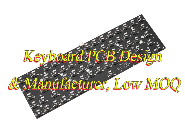
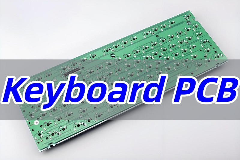
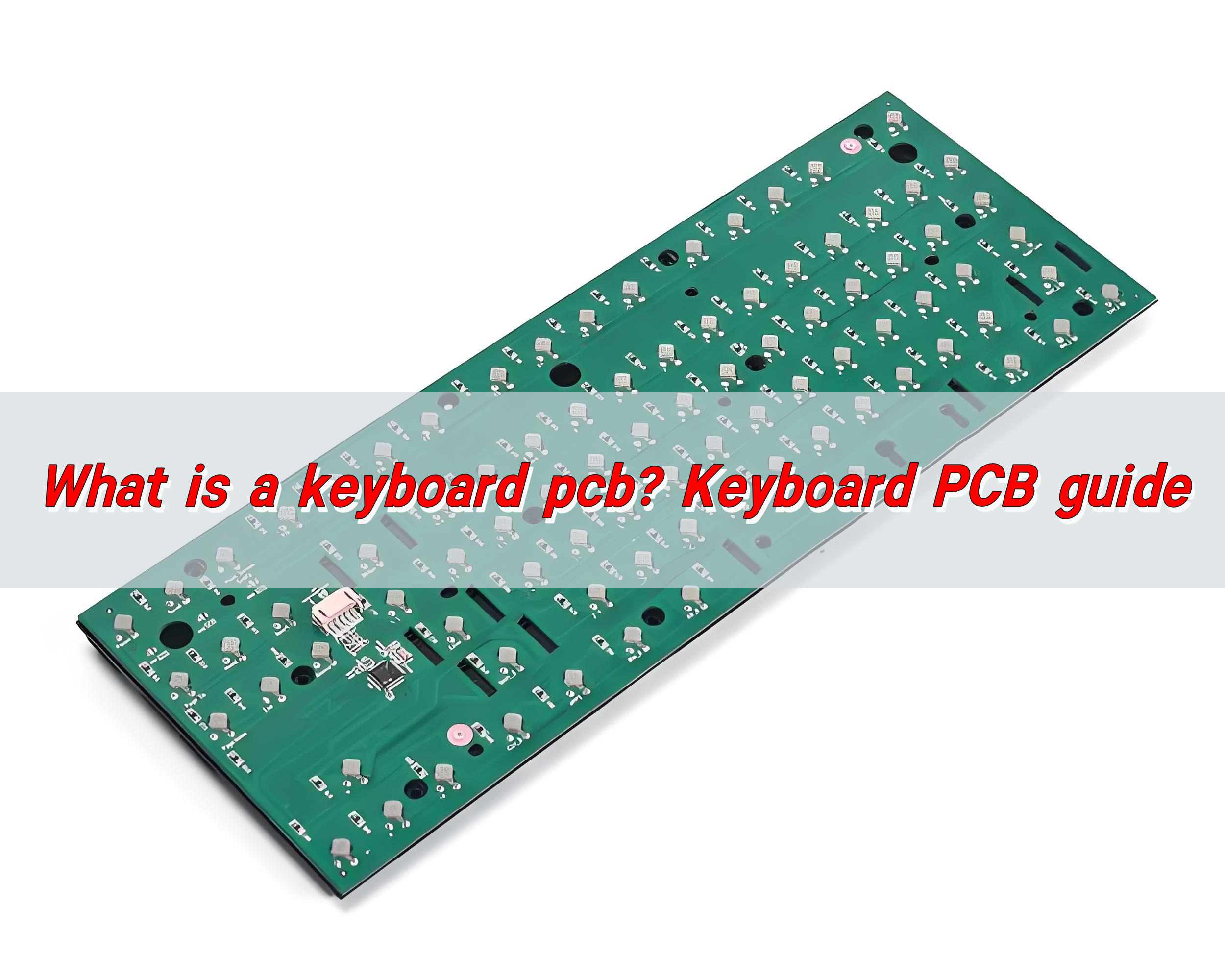
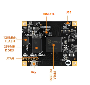
A keyboard PCB is the electronic backbone of a keyboard. It is a printed circuit board that detects each key press and converts it into a digital signal the device can understand. Every time a key is pressed, the PCB closes a circuit, identifies the key’s position, and sends accurate input data to the computer.
What Is a PCB on a Keyboard?
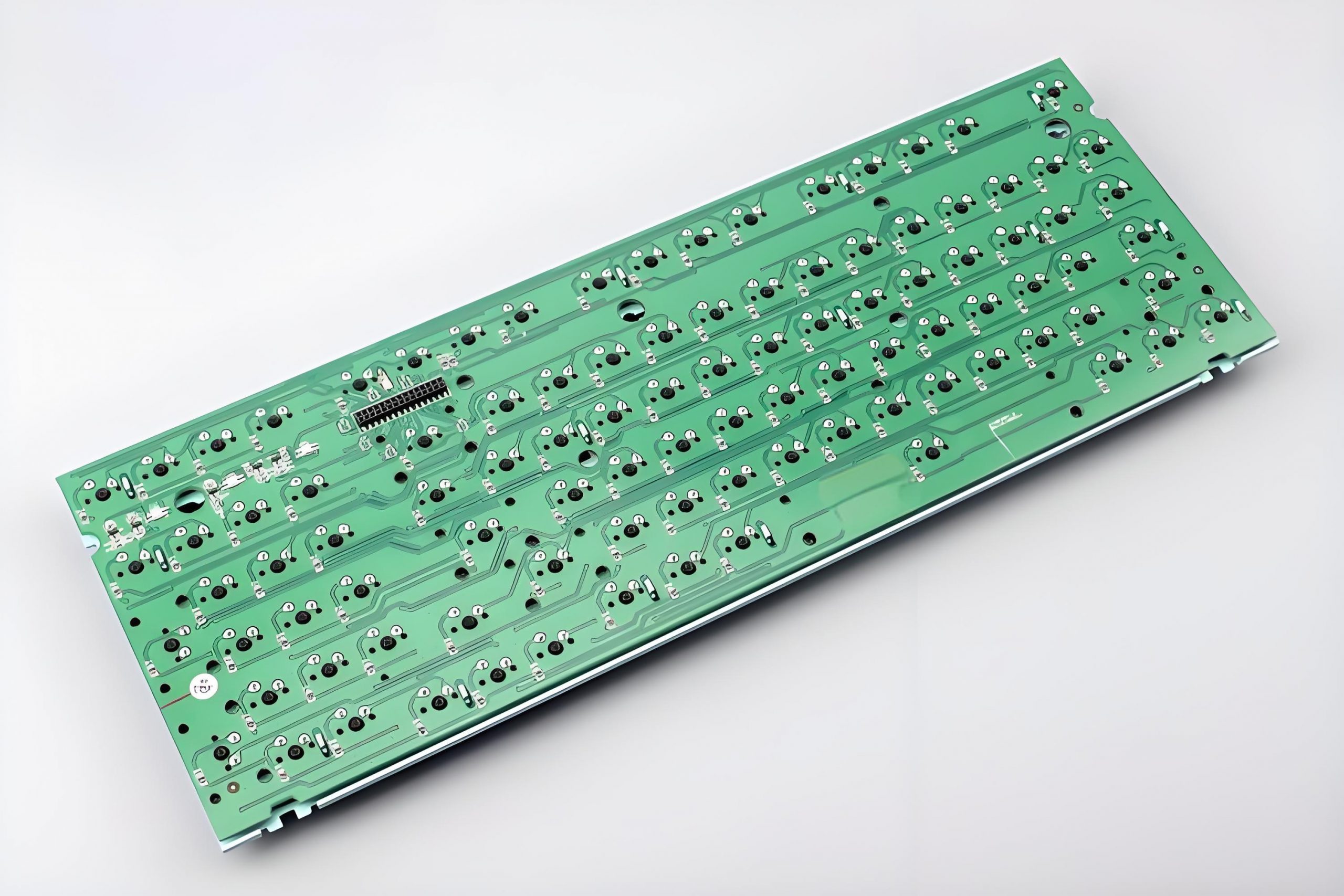
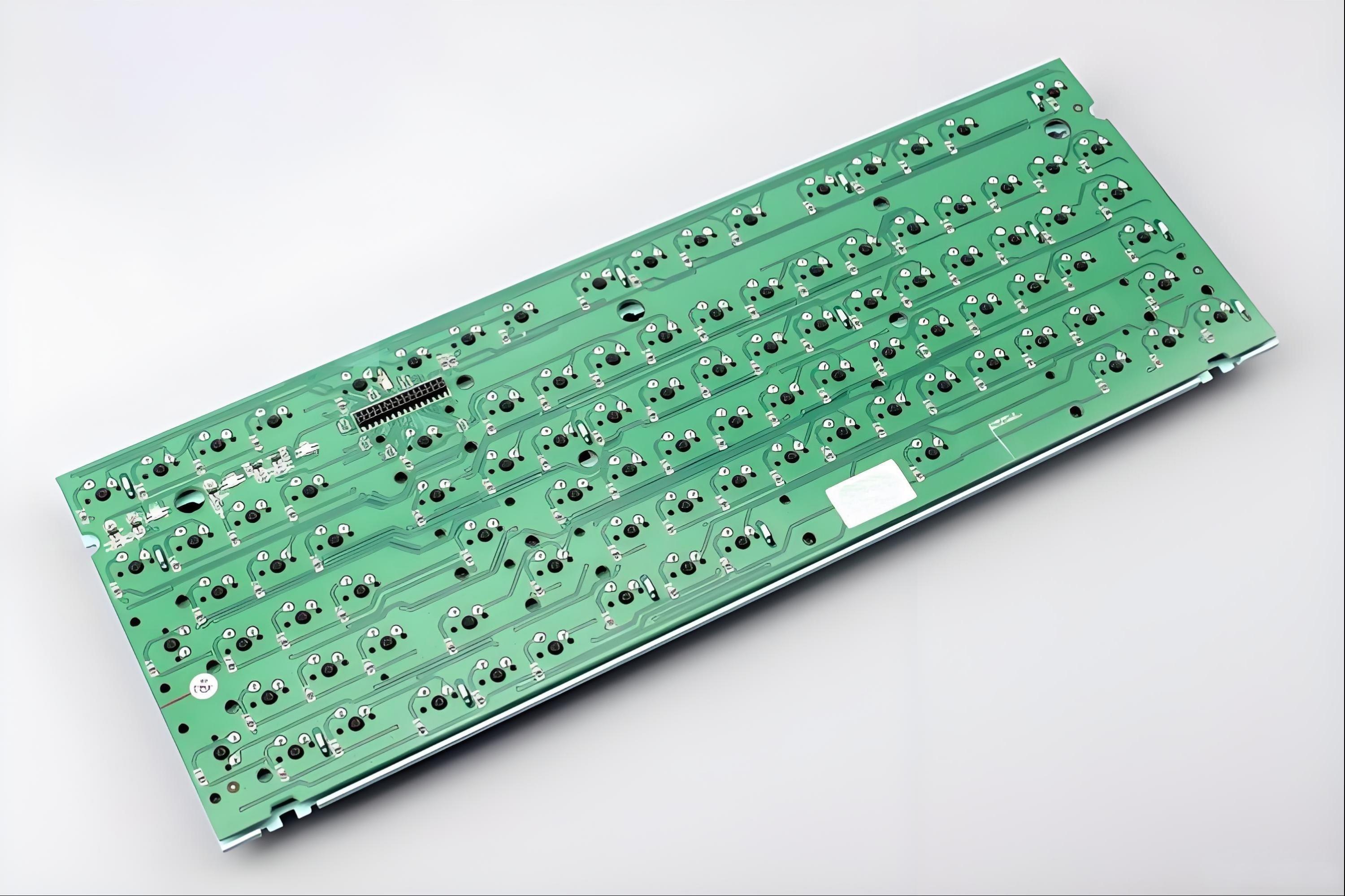
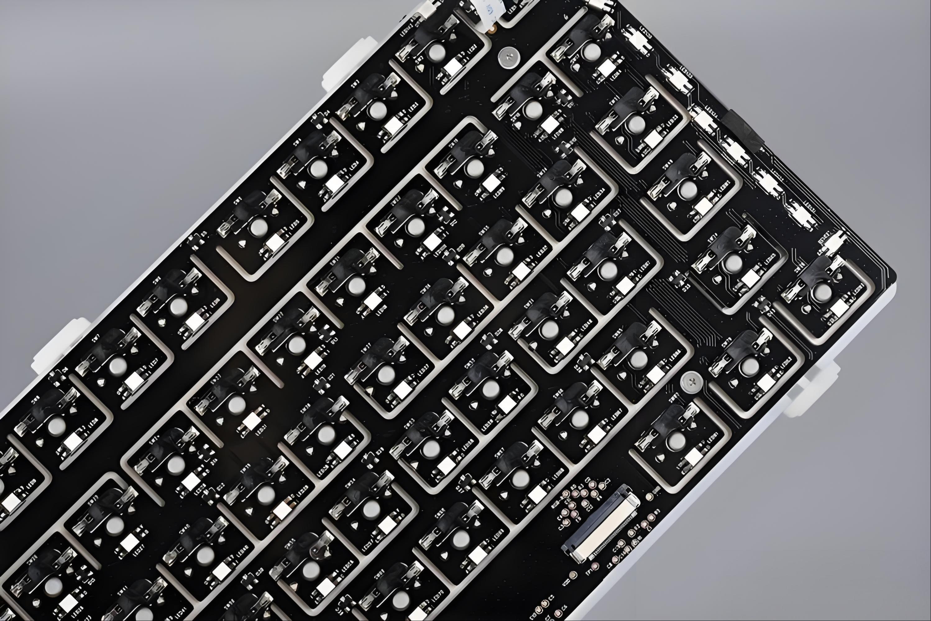
A keyboard PCB is the printed circuit board that connects switches, stabilizers, LEDs, and the controller into one stable platform. Each time you press a key, the switch closes a circuit on the PCB, sending an electrical signal to the microcontroller. That signal becomes the character, function, or macro you see on your screen.
The PCB replaces old-style wiring that was once messy and inconsistent. Instead, everything sits on a neat, flat board where copper traces interpret the user’s input. Because these traces are organized and protected, the keyboard responds more smoothly and lasts longer.
In mechanical keyboards, the PCB is more advanced. It handles precise actuation, varied layouts, backlighting, and programmable features.
A keyboard PCB also influences these factors:
- Typing feel due to layout support and switch connection method.
- Durability due to copper thickness, plating quality, and protection layers.
- Signal stability because clean traces reduce interference.
- Lighting effects when the PCB includes addressable RGB pads.
Customization freedom when the board offers hot-swap sockets or multiple layout footprints.
What Is a Magic Keyboard PCB?
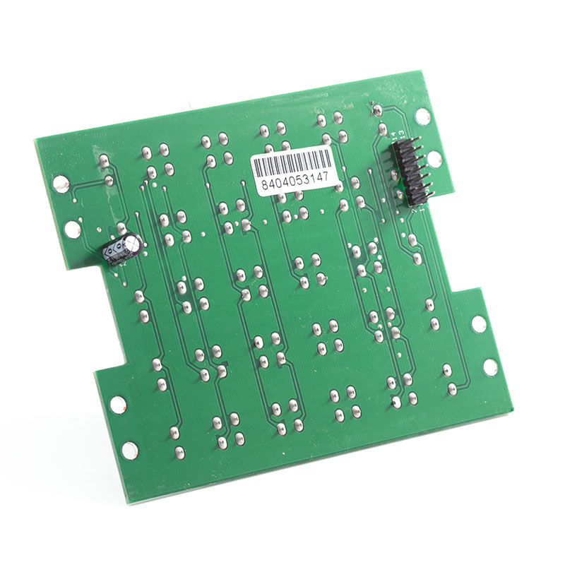
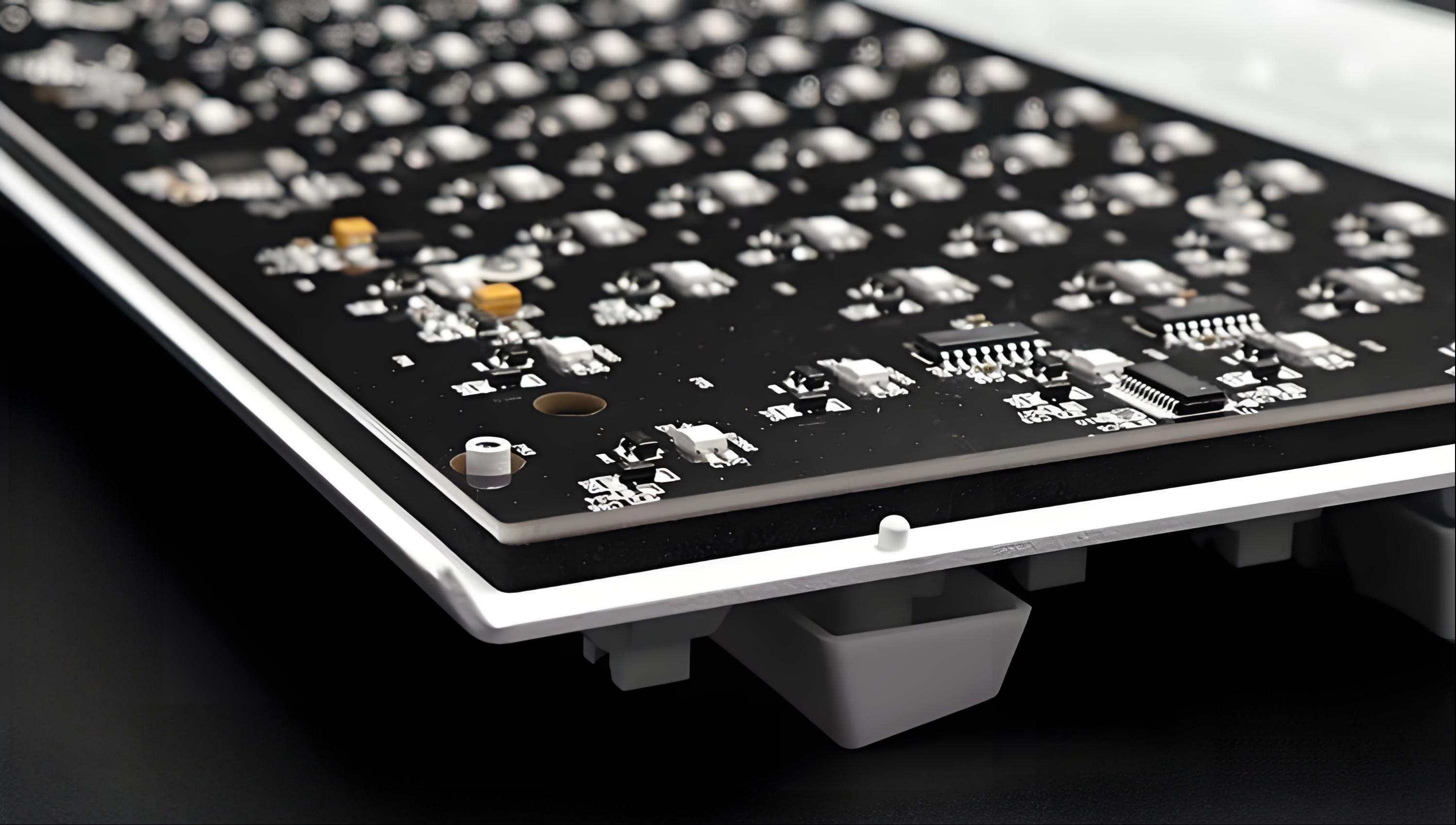
Magic Keyboard PCB refers to the internal printed circuit board used in Apple’s Magic Keyboard line. It is a compact, low-profile PCB designed to support thin scissor switches, stable key feel, and low-power Bluetooth operation. While it follows the same core idea as a standard keyboard PCB, its structure is tighter, slimmer, and more integrated.
Unlike many mechanical keyboard PCBs, a Magic Keyboard PCB does not support modular changes. The layout is fixed. The switches are low-profile scissor mechanisms, and the board follows Apple’s proprietary design.
A Magic Keyboard PCB uses tight copper routing, small SMD components, and a compact controller area. Each key pad is reinforced to keep signals stable even under heavy typing. The board often includes Bluetooth antennas, battery connections, and power-efficient circuitry that keeps the keyboard running for long periods.
How to Check if a Keyboard PCB Is Working?
Checking if a keyboard PCB works is simple when you follow a clear process. You can test your board with basic tools, and each step helps you find problems early. A working PCB reacts fast, sends clean signals, and shows no unusual behavior when keys are pressed.
Here is a practical sequence you can follow.
- First, connect the keyboard PCB to your computer.
Use a USB cable. If the board lights up or if the system plays a connection sound, you know the controller is active.
- Next, open a keyboard testing tool online.
There are many free testing websites. If each key registers, the keyboard PCB is working well.
- Then, check the LEDs or RGB pads.
If your PCB includes lighting, turn it on through the firmware.
- After that, inspect the USB connector area.
A loose connector can cause random disconnects. Light pressure on the port should not break the connection.
- Finally, test the board again after assembling it into a case.
A case may add pressure to certain components.
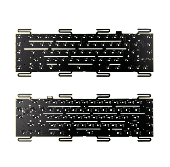
How to Design a Keyboard PCB?
To design a keyboard PCB, you can follow a structured approach that keeps the process simple.
- Start with your layout.
Choose the size you want: 60%, 65%, TKL, full-size, or a custom shape. The layout decides the switch spacing, stabilizer placement, and the overall PCB outline.
- Move to the switch footprints.
Mechanical keyboard PCBs usually use MX-style footprints. If you want a low-profile build, you may use Choc footprints.
- Add the controller.
Popular microcontrollers include Atmel ATmega32U4, RP2040, STM32, and other modern chips.
- Plan the matrix wiring.
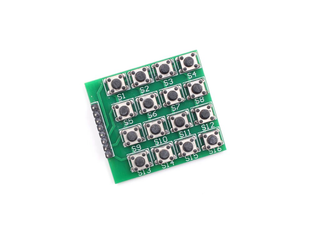
The matrix is a grid of rows and columns. It helps the controller read key inputs efficiently.
- Include diodes.
Each switch pad usually needs a diode to prevent ghosting.
- Add RGB or LED pads if needed.
Per-key RGB or under-glow lighting adds visual style.
- Check grounding and shielding.
A stable grounding layer keeps signals clean. It also reduces interference in high-speed USB communication.
- Finally, export your files.
You will need Gerber files, a drill file, and a BOM.
How to Make a Keyboard PCB?
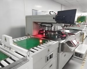
Making a keyboard PCB involves fabrication steps that follow your design file. Good manufacturing practice ensures stable traces, strong plating, and consistent performance.
The following steps explain the process of manufacturing a keyboard PCB.
- Prepare your files: Send Gerber files, drill files, a layer stack, and your BOM to a PCB manufacturer.
- Choose suitable materials: Most keyboard PCBs use FR4. If you want extra durability or thin form factors, you can choose special materials.
- Confirm layer count: Most keyboard PCBs are 1-layer or 2-layer boards. If you use complex lighting or advanced controller circuits, you may choose a 4-layer design.
- Move to fabrication: The manufacturer prints copper patterns, drills holes, plates vias, and builds the board with protective solder mask and silkscreen.
- Add surface finish: HASL, ENIG, or ENEPIG are common finishes.
- Apply quality checks: The finished board goes through electrical testing to confirm that every trace works.
Send the PCB to assembly if needed, If you want SMD components pre-assembled, BEST Technology can solder the controller, resistors, capacitors, and LEDs.
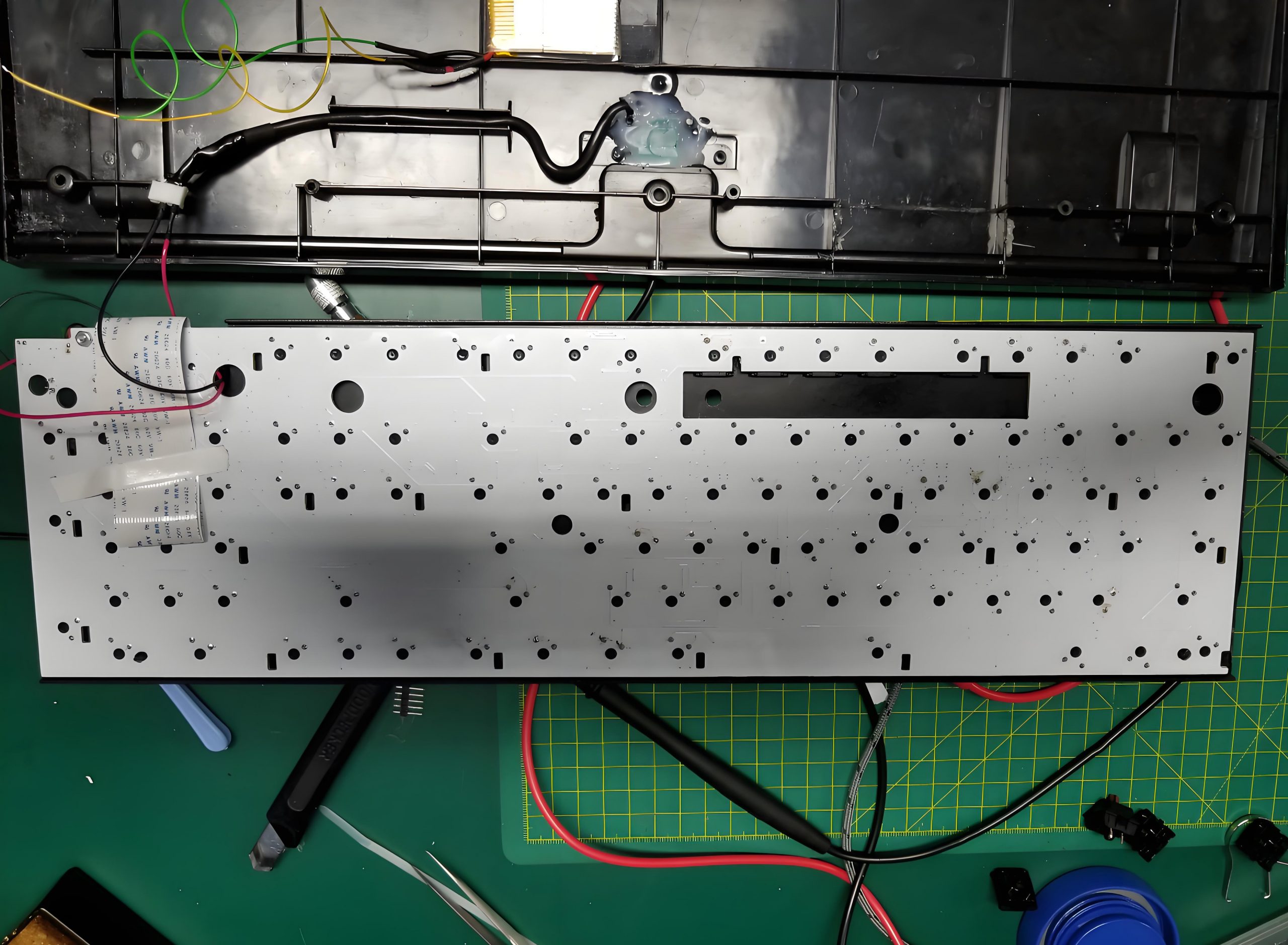
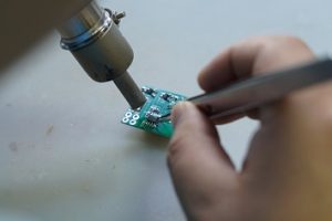
How to Solder a Keyboard PCB?
Before you begin, gather a soldering iron, solder wire, tweezers, and a small amount of flux. Keep the workspace clean.
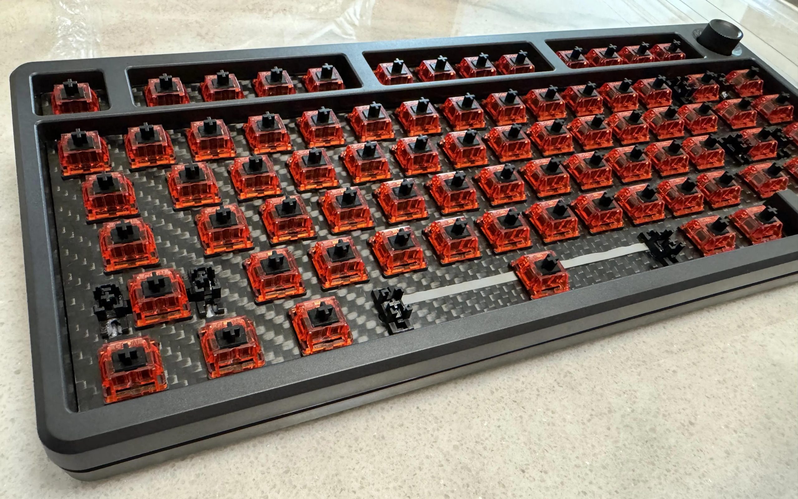
If your layout uses screw-in stabilizers, install them first. They sit lower than switches and must be secured before anything else.
If your PCB is not a hot-swap board, insert each switch through the plate and into the PCB. Make sure the pins are straight. Each one must sit firmly in the holes.
A temperature around 320–350°C works well for most solder wires. Let the iron warm up fully before you begin. Hold the iron so it touches both surfaces. Then feed a small amount of solder. Move from one side to the other. If your PCB includes LEDs, solder them next. Once the soldering is complete, let the board cool.
How to Clean a Keyboard PCB?
Cleaning a keyboard PCB keeps it fresh, stable, and long-lasting. Dust, flux residue, or spilled liquid may affect the board over time.
First, disconnect the PCB from power. Make sure no USB cable or battery is connected. Use compressed air. Short bursts keep the PCB clean without harming components.
Use isopropyl alcohol (IPA). Apply it to a cotton swab or a soft brush. IPA removes fingerprints, flux residue, and sticky dirt. A small amount is enough. Too much liquid may trap moisture under components. Alcohol dries fast. Leave the board in open air for a few minutes. A dry PCB stays safe and ready for testing.
If you use the keyboard in a humid place, cleaning becomes even more important. Regular cleaning helps the traces stay fresh and stable.
Why Choose EBest Circuit (Best Technology) for Keyboard PCB Manufacturing?
EBest Circuit (Best Technology) delivers engineering support, stable fabrication, and consistent quality, which gives users and brands more confidence throughout the entire process. Our team focuses on accuracy, smooth communication, and clean workmanship so your project runs without stress.
If you need unique switch layouts, alternative footprints, or special routing, we provide DFM guidance to make your files easier to produce. Mechanical keyboard PCBs often need ENIG for smooth soldering, stable plating, and long-term durability.
Conclusion:
A keyboard PCB shapes how a keyboard responds, how long it lasts, and how enjoyable it feels. We help you design, produce, assemble, and test keyboard PCBs with smooth communication and consistent results.
For project support or inquiries, please contact us at sales@bestpcbs.com