Copper inlay PCB is a special circuit design method that significantly improves heat dissipation capability and current loading performance by inlaying copper in a PCB. This technology is widely used in power electronics, automobile electronics, and GaN devices, helping to tackle the difficult heat management problem of traditional PCBs in high-power and high-density environments.
Do you suffer from these headaches?
- Poor heat dissipation problem in traditional PCBs?
- High manufacturing difficulty and cost issues, such as easy to have alignment issues and material waste?
- The compatibility problem between design and manufacturing? For example, in design, there may be a compatibility problem between the inlay copper structure and the other parts of the PCBs, such as the layer alignment, hole diameter, and the edge treatment, which finally leads to the manufacturing difficulty increasing.
- Problems with the material selection and cost?
Here are some real solutions EBest Circuit (Best Technology) uses in customers’ projects.
- Optimizing design and manufacturing process: EBest Circuit (Best Technology) adopts high-precision manufacturing processes, such as laser etching or photolithography.
- Optimizing material selection: We use high-purity copper material to improve conductivity and mechanical performance. Besides, select a copper substrate or an aluminum substrate to improve thermal dissipation performance and reliability.
- Controlling costs and boosting manufacturing: EBest Circuit (Best Technology) optimizes design to reduce material waste and manufacturing complexity.
- Optimizing heat dissipation and thermal management: We employ a multilayer copper inlay structure to boost the thermal dissipation capability
EBest Circuit (Best Technology) provides copper inlay PCB design optimization, prototype, mass production, and assembly service. We have productive experience to tackle the thermal dissipation problem, manufacturing difficulty, and material selection issues. If you have any technical questions or doubts, a warm welcome to get in touch with us at sales@bestpcbs.com.
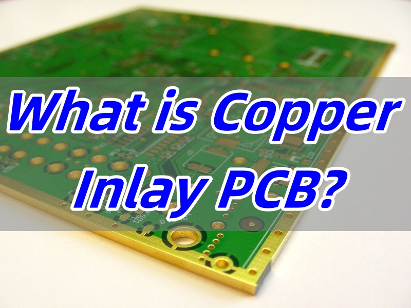
What is copper inlay PCB?
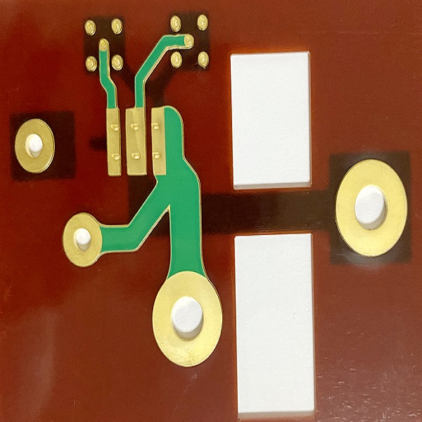
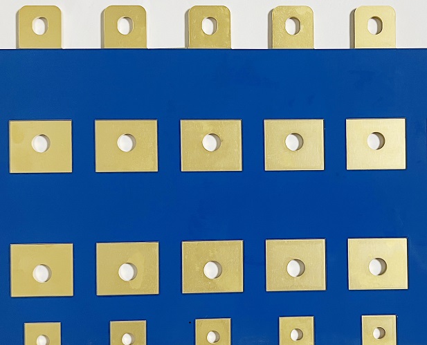
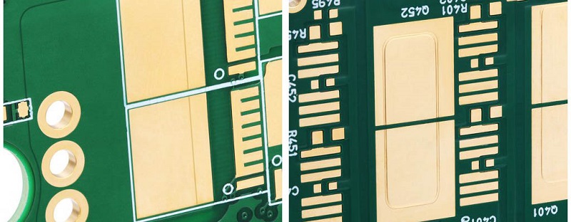
Copper inlay PCB integrates solid copper pieces into specific areas of a PCB. It benefits to improve conductivity capability and quick heat dissipation performance. In high current or high power applications, this design is more reliable than the design that purely make the thicker copper layer.
What is the relation: PCB inner layer copper thickness, copper inlay PCB?
The PCB inner layer copper thickness directly affects the board’s electrical and thermal behavior. It is good to know that if purely depending on copper thickness can’t meet demands in high power applications, then copper inlay PCB has a key role here. It boosts the copper thickness and quality in the part area, so as to improve the performance of the current load and heat dissipation.
| Aspect | PCB Inner Layer Copper Thickness | Copper Inlay PCB |
| Definition | Standard copper thickness used across PCB inner layers | Embedded solid copper blocks in selective PCB areas |
| Main Role | Supports current flow and basic thermal paths | Handles high current and localized heat dissipation |
| Application | General PCB design, balanced power distribution | High-power, high-density, or thermally stressed zones |
| Performance Impact | Limited by overall copper thickness | Significantly boosts current and thermal capability |
What is difference: copper inlay PCB, copper pour in PCB?
Copper inlay and copper pour are different strategies. Copper pour in PCB generally is for large area grounding or power distribution; however, copper inlay PCB is for the part area strengthening. The former one is limited to copper thickness, and its heat dissipation capability is limited. However, the latter one conducts heat directly via a solid copper block, and its effect is more significant.
| Aspect | Copper Inlay PCB | Copper Pour in PCB |
| Material | Solid copper blocks inserted into PCB cavities | Large copper area formed by plating during PCB process |
| Purpose | Localized thermal control and high-current pathways | Power planes, ground planes, signal return paths |
| Precision | Highly targeted in selected PCB zones | Spread across wide board sections |
| Thermal Efficiency | Superior, due to direct copper mass and conduction | Limited by copper thickness and plane size |
Why do PCBs use copper inlay?
PCB using copper inlay to mainly tackle the problem of the heat dissipation bottleneck and the current overloading. As the device is getting smaller and smaller while the power is getting larger and larger, the traditional PCB copper layer is easy to overheat, leading to failure. Copper inlay technology provides a stable thermal path and the current route, which reduces the failure rate and extends the product lifespan radically.
How to inlay copper into PCB?
- The fabrication process includes copper block cutting → inlaying it into the PCB cavity → lamination bonding → common drilling, plating, and the etching process.
In this way, it not only ensures the bonding between the copper block and circuit boards but also ensures the surface smoothness and the overall heat conductivity effect. In actual production, it may need to adjust the process according to the specific parameters, such as copper block thickness and substrate types.
What is the Copper inlay PCB price?
Copper inlay PCB price depends on the board’s size, design complexity, and copper block quantity. Although the cost is higher than a common PCB, in high-power applications, it will reduce the repair and maintenance costs significantly due to the good heat dissipation. Hence, from the whole lifespan cost, it will be more cost-effective.
What are the advantages of GaN device thermal with copper inlay PCB in high-power applications?
A GaN device thermal with copper inlay PCB gives engineers a way to manage extreme heat and high currents. And it takes center stage in the high-power applications.
- The high efficiency of heat conductivity in the PCB minimizes the risk of GaN devices overheating, supporting consistent performance even under demanding conditions.
- Enhanced heat management ensures more stable high-frequency operation and improves switching performance, making the device suitable for rigorous tasks.
- The copper inlay PCB enables the device to handle higher current densities without performance loss or overheating.
- Keeping reliable operation in the compact design.
- Extending the lifespan of the device and reducing the heat stress.
How does PCB copper inlay improve heat dissipation?
PCB copper inlay offers a direct heat dissipation path for the key heating components. The specific performance is as follows:
- Rapidly conduct heat into the copper layer or heat sinks.
- Reduce the operation temperature of the key components.
- Reduce hotspots and protect the sensitive devices.
- Improve the integrated power efficiency and stability.
- Extend the operation lifespan of circuit boards.
In summary, copper inlay PCB is a workable solution to tackle the problem in the heat dissipation of the high-power and high heat density applications, and in the electrical performance. EBest Circuit (Best Technology) wins customers’ trust and repeat orders since our team not only ensures customers get reliable and high-performance circuit boards via our rigorous quality control and rapid lead time, but also provides high-quality solutions. If you have any new projects, just feel free to contact us for a free DFM analysis, quick prototype, full turnkey fabrication, assembly, and box build service at sales@bestpcbs.com.