PCB manufacturing PCB manufacturing
Home > Blog

Posts Tagged ‘bnc connector pcb mount’

Reliable BNC PCB Solutions for Precision RF Connectivity
Tuesday, December 2nd, 2025

BNC PCB refers to the integration of BNC (Bayonet Neill–Concelman) connectors directly onto printed circuit boards, providing a robust interface for RF (radio frequency) signals in applications ranging from test equipment to communication devices. This article explores the types, selection criteria, layout practices, and performance considerations for implementing BNC connectors on PCBs, with a focus on achieving reliable high-frequency connectivity.

Are you struggling with signal loss, impedance mismatches, or mechanical instability in your RF designs? Many engineers face recurring challenges when integrating coaxial interfaces like BNC connectors onto PCBs. Common frustrations include:

  • Poor impedance continuity leading to signal reflections and degraded performance.
  • Mechanical strain causing connector loosening or PCB pad damage.
  • Inadequate grounding strategies that increase electromagnetic interference (EMI).
  • Difficulty selecting the right connector type (vertical, right-angle, or edge-mount) for spatial and electrical needs.
  • Time-consuming prototyping cycles due to footprint or layout errors.

These issues can be systematically addressed with thoughtful design and manufacturing support. Here’s how a specialized PCB provider can help:

  • Impedance-controlled routing ensures minimal signal distortion from connector to trace.
  • Robust anchoring features (like through-hole pins or metal brackets) enhance mechanical stability.
  • Optimized ground plane design and via fencing reduce EMI and crosstalk.
  • Expert guidance on connector selection based on frequency, space, and mounting orientation.
  • Rapid prototyping services with validated footprints to accelerate development.

At BEST Technology, we specialize in high-frequency PCB solutions, including precision-engineered BNC interconnects. Our team supports your design with impedance-matching expertise, durable board materials, and fast turnaround for prototypes and production. A warm welcome to contact us at sales@bestpcbs.com to discuss your project requirements.
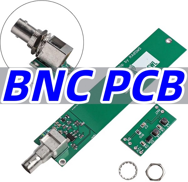
BNC PCB

What is a BNC PCB?

A BNC PCB incorporates a BNC connector—typically a BNC PCB connector—directly mounted to the board, serving as a coaxial interface for RF signals. These connectors use a bayonet coupling mechanism for quick, secure connections and are designed to maintain a 50-ohm or 75-ohm characteristic impedance.

  • Signal Support:
    The BNC PCB connector preserves signal integrity by providing a shielded path from the cable to the PCB traces.
    Its coaxial structure minimizes EMI, while the board layout ensures impedance continuity between the connector’s center conductor and the microstrip or stripline transmission line.
  • Applications:
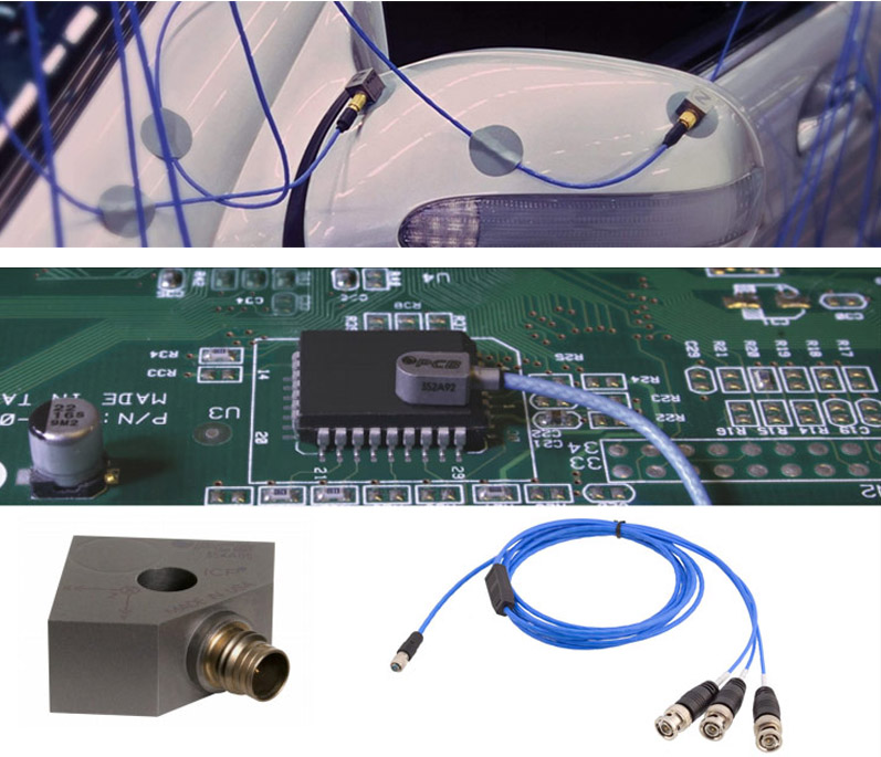
    Commonly used in video equipment, RF test instruments, and data communication systems where frequent connection cycles and RF performance are critical.
    In summary, a BNC PCB enables efficient RF signal transition between external cables and internal circuitry, with careful attention to impedance matching and shielding.
BNC PCB

​What Types of BNC Connector PCB Mount Options Are Most Common in RF Boards?

Engineers can choose from several mounting styles, each suited to different mechanical and spatial constraints.

  • Vertical Mount (BNC PCB mount):
    The connector stands perpendicular to the board, ideal for applications where space is limited in the horizontal plane.
  • Right-Angle Mount (BNC connector PCB mount right angle):
    The connector body parallels the board, saving vertical height—useful for compact modules or stacked assemblies.
  • Edge Mount (BNC edge mount PCB):
    Installed on the board’s edge, often used when the connector must align with an enclosure panel.
  • Surface-Mount or Through-Hole:
    Through-hole versions offer stronger mechanical retention, while surface-mount types suit automated assembly.
    The BNC connector PCB mount style is selected based on layout density, cable orientation, and shielding requirements.

How Do You Choose the Right BNC Female PCB Mount Connector for Your Design?​

Selecting the appropriate BNC female PCB mount connector involves evaluating electrical, mechanical, and environmental factors.

  • Impedance: Ensure the connector matches the system impedance (e.g., 50 ohms for most RF applications).
  • Frequency Range: Standard BNC connectors perform up to 4 GHz; verify the model’s rated frequency.
  • Mounting Style: Choose vertical, right-angle (BNC female right angle solder PCB mount connector), or edge-mount based on space and cable routing.
  • Termination Type: Soldering (through-hole or surface-mount) vs. crimping; through-hole provides better strain relief.
  • Material and Plating: Brass with gold or nickel plating ensures corrosion resistance and stable conductivity. A well-chosen BNC female PCB connector minimizes VSWR (voltage standing wave ratio) and withstands mating cycles.

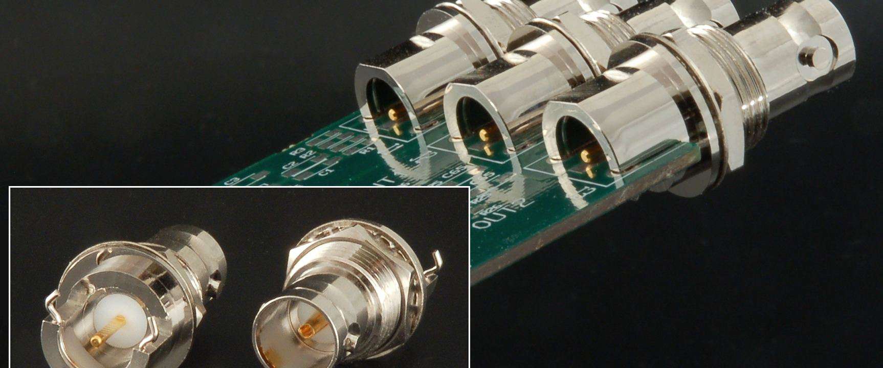
What Layout Rules Matter Most When Creating a Reliable BNC Connector PCB Footprint?​

The BNC connector PCB footprint must maintain impedance integrity and mechanical stability. Key rules include:

  • Impedance Matching: Design the pad pattern and adjacent ground structures to match the connector’s characteristic impedance (e.g., 50 ohms).
  • Grounding: Place grounding vias near the connector’s shield pins to create a low-inductance path to the ground plane.
  • Pad Size and Shape: Follow the manufacturer’s datasheet to avoid tombstoning or solder voids.
  • Keep-Out Zones: Avoid placing components or traces under the connector body to prevent short circuits.
  • Strain Relief: Include metal anchors or epoxy trenches for high-vibration environments. A precise BNC PCB footprint is critical for signal fidelity and long-term reliability.

When Should Engineers Use a BNC Right Angle PCB Mount Instead of a Vertical One?​

A BNC right angle PCB mount is preferred when:

  • Vertical Space is Limited:
    Such as in slimline instruments or stacked PCBs.
  • Cable Routing Constraints:
    The cable must exit parallel to the board to avoid sharp bends.
  • Panel-Mount Alignment:
    The connector interfaces with a side-panel port. In contrast, a vertical BNC PCB mount is better when cables connect from above, as in rack-mounted equipment.
    The right-angle version (90 degree BNC PCB mount) reduces mechanical leverage on the PCB, lowering the risk of pad lifting.

How Does an Ultra-Tiny BNC Jack PCB Help in Compact RF Modules?​

An ultra-tiny bnc jack pcb(e.g., sub-miniature versions) saves space without sacrificing performance. Benefits include:

  • High Density: Enables more connectors per board area in portable devices.
  • Lightweight Design: Critical for aerospace or handheld instruments.
  • Preserved Performance: Maintains impedance control and shielding despite smaller dimensions. These jacks are ideal for high-density RF systems like multi-channel data acquisition boards.

What Routing Practices Improve Performance When Working With a 90 Degree BNC PCB Mount?​

For a 90 degree BNC PCB mount, follow these routing guidelines:

  • Impedance Continuity: Use controlled-impedance traces from the connector pin to the IC, avoiding abrupt width changes.
  • Minimal Stub Length: Keep the transition from the connector pad to the main trace as short as possible.
  • Ground Plane Integrity: Ensure an unbroken ground plane beneath the trace; add grounding vias near the connector.
  • Avoid Sharp Bends: Use curved or 45-degree trace bends to reduce reflections. Proper routing ensures that the BNC right angle PCB maintains low VSWR and insertion loss.
BNC PCB

Why Do RF Teams Rely on Best Technology for BNC Prototype PCB Production?​

RF teams choose Best Technology for BNC prototype PCB manufacturing due to:

  • Impedance Expertise: We control dielectric thickness and trace geometry to achieve precise impedance matching.
  • High-Frequency Materials: Expertise with Rogers, Taconic, or FR-4 hybrids for optimal RF performance.
  • Rapid Prototyping: Quick-turn services with validated designs to accelerate testing.
  • Quality Assurance: Rigorous testing for VSWR, insertion loss, and mechanical stability. Our capability to produce reliable BNC prototype PCB assemblies reduces iteration cycles and ensures performance compliance.

In a nutshell, BNC PCB solutions enable precise RF connectivity by integrating robust coaxial interfaces directly onto circuit boards. This guide has detailed connector selection, layout techniques, and routing practices to ensure signal integrity in high-frequency designs. At BEST Technology, we combine engineering support with advanced manufacturing to deliver reliable BNC PCBs for prototyping and production. Pls feel free to reach out to us at sales@bestpcbs.com for your next RF PCB project.

FAQs about BNC PCB

Is BNC better than SMA?

  • BNC offers quick bayonet coupling for frequent connections but is typically rated to 4 GHz. SMA uses a threaded interface for higher frequencies (up to 18 GHz) and better EMI shielding. Choose BNC for ease of use in lower-frequency applications.

Is BNC better than Ethernet?

  • BNC is designed for RF signals (e.g., video, radio), while Ethernet (RJ45) carries digital data. They serve different purposes; BNC provides superior impedance control for analog RF.

Is BNC the same as RF?

  • BNC is a type of RF connector. “RF” is a broad term for radio frequency signals, while BNC refers to a specific connector family commonly used for RF interconnects.

How to crimp a BNC?

  • Strip the coaxial cable to expose the center conductor and shield. Insert the center conductor into the connector pin and crimp. Slide the shield braid over the body, and crimp the outer sleeve. Use a BNC crimping tool for consistent results.

How to Choose the Best BNC PCB?
Monday, November 17th, 2025

BNC PCB​ refers to the integration of Bayonet Neill–Concelman connectors directly onto a printed circuit board, providing a robust and reliable interface for coaxial RF connections. This article provides a comprehensive guide on selecting the right BNC connector PCB by examining types, mounting styles, design rules, and performance criteria to ensure optimal signal integrity for your application.

Selecting the right ​BNC PCB connector​ is critical, yet many engineers face significant challenges that can derail a project’s performance and timeline.

  • Intermittent Signal or Loss:​​ Choosing a connector with an incorrect impedance (e.g., 50-ohm vs. 75-ohm) or poor-quality coaxial interface leads to signal reflections, data corruption, and degraded performance in high-frequency applications.
  • Mechanical Failure in Demanding Environments:​​ Standard ​BNC PCB mount​ connectors can loosen, break, or detach from the board when subjected to vibration, shock, or frequent mating cycles, causing system failures.
  • Incorrect Footprint Leading to Assembly Issues:​​ An inaccurate ​BNC connector PCB footprint​ can cause misalignment during SMT assembly, resulting in poor soldering, short circuits, or the need for costly board rework.
  • Space Constraints Limiting Design:​​ Finding a suitable connector for ultra-compact devices is difficult; a standard ​BNC female PCB mount​ might not fit, forcing undesirable design compromises.
  • Poor Performance at High Frequencies:​​ Many standard ​PCB BNC connectors​ are not characterized for microwave frequencies, leading to unexpected insertion loss and VSWR (Voltage Standing Wave Ratio) that hamper the performance of sensitive RF systems.

Fortunately, these challenges can be effectively mitigated through informed selection and design practices. The following ​targeted solutions for reliable BNC PCB integration address these pain points directly.

  • ​​Specify Impedance and Frequency Upfront:​​ Always verify if your application requires a 50-ohm or 75-ohm ​coaxial BNC PCB​ and select a connector rated for your maximum operating frequency to ensure signal integrity.
  • Opt for Robust Mounting Styles:​​ For harsh environments, choose a ​BNC PCB mount​ style with robust mechanical features, such as threaded bushings or four-hole flange mounting, to secure the connector firmly to the board and chassis.
  • Utilize Certified PCB Footprint Models:​​ Work with suppliers who provide certified, tested ​BNC connector PCB footprint​ and layout recommendations, including a ​BNC female PCB mount vertical 3D model, to prevent DFM (Design for Manufacturability) issues.
  • Select Space-Efficient Form Factors:​​ For tight spaces, utilize an ​ultra-tiny BNC jack PCB​ or a ​BNC right angle PCB mount​ connector to save valuable board real estate and maintain a low profile.
  • Choose Connectors with Characterized HF Performance:​​ For RF applications, select ​BNC PCB connectors​ that come with S-parameter models (S2P files) to simulate and validate high-frequency performance in your design environment.

As a specialized PCB and assembly manufacturer, BEST Technology provides not only high-quality ​cable adapters BNC PCB​ solutions but also expert DFM support. We help you navigate these critical choices to ensure your ​PCBA projects​ are built for reliability and performance from the ground up. For a consultation, pls feel free to contact us at sales@bestpcbs.com.

BNC PCB

What is a BNC PCB?​

A BNC PCB is a circuit board that incorporates a BNC connector, a common type of RF coaxial connector known for its quick-connect bayonet coupling mechanism. This integration allows the board to interface with coaxial cables for transmitting radio frequency signals up to several GHz. They are ubiquitous in applications requiring stable signal transmission, such as test and measurement equipment, video broadcasting, data acquisition systems, and telecommunications infrastructure.

  • Function:​​ The primary function is to provide a shielded, impedance-matched transition between a coaxial cable and the traces on the PCB, minimizing signal loss and electromagnetic interference (EMI).
  • Importance:​​ A well-chosen ​PCB​ BNC is fundamental to maintaining signal integrity, which is the quality of an electrical signal. A poor connector choice can degrade the signal, leading to errors and reduced system performance.

What are the Types of BNC Connector PCB?​

BNC connectors for PCBs come in various types, primarily categorized by gender, impedance, and termination style. Choosing the correct type is the first step in the selection process.

  1. ​By Gender and Mounting:​
    • BNC Female PCB Mount:​​ This is the most common type, where the jack is soldered onto the board. It interfaces with a plug (male) on the cable end. Options include ​BNC female PCB mount vertical​ and ​BNC female PCB mount right angle.
    • BNC Male PCB Mount:​​ Less common, this connector has the pin and is soldered to the board, mating with a female jack on the cable.
  2. ​By Impedance:​
    • 50-ohm BNC PCB:​​ The standard for most RF and digital data applications. It provides a good balance between power handling and low loss.
    • 75-ohm BNC PCB:​​ Primarily used in video signaling (e.g., SDI), audio, and telecommunications where impedance matching to 75-ohm coaxial cable is critical. Using a 50-ohm connector on a 75-ohm line will cause signal reflections.
  3. ​By Form Factor:​
    • Standard PCB Mount BNC Connector:​​ The typical size found on most equipment.
    • Mini BNC PCB and Micro BNC PCB:​​ Smaller versions designed for high-density applications where board space is at a premium, such as in compact data acquisition systems.

How Many Ways of BNC Connector PCB Mount can be Used in Your Design?​

The mounting style directly impacts the mechanical robustness and assembly of your ​BNC connector for PCB board. There are three primary ways to mount a BNC connector.

  • Through-Hole Mounting:​​ The connector has leads that are inserted into drilled holes on the PCB and soldered. This method offers the strongest mechanical bond, making it ideal for applications subject to high mating force or vibration. However, it requires more board space and is not suitable for high-density designs.
  • Surface-Mount (SMT):​​ The connector is soldered to pads on the surface of the PCB. SMT is the standard for automated assembly, allowing for smaller board sizes and higher component density. An ​ultra-tiny BNC jack PCB​ is typically SMT. While mechanically weaker than through-hole, proper design with anchoring pads can ensure sufficient strength.
  • Press-Fit Mounting:​​ The connector is pressed into a plated-through hole in the PCB, creating a gas-tight connection without solder. This is a highly reliable method used in severe environments with extreme temperature cycling, as it eliminates solder joint fatigue.

What are the Functions of Ultra-tiny BNC Jack PCB in Modern Electronics?​

The ​ultra-tiny BNC jack PCB​ is a specialized component designed to fulfill critical roles in today’s increasingly miniaturized electronics.

  • Space Conservation:​​ Its primary function is to provide a full-featured RF interface in extremely limited space, enabling the design of compact devices like portable oscilloscopes, mini-PCs, and dense server blades.
  • High-Density Interconnects:​​ It allows designers to pack multiple RF ports side-by-side on a single board, which is essential for multi-channel systems like data acquisition cards and switch matrices.
  • Portable and Handheld Equipment:​​ These connectors are indispensable for battery-operated, handheld test gear and medical devices where every cubic millimeter counts, without sacrificing the performance of a standard BNC interface.

How to Select Coaxial BNC PCB for Your Projects?​

Selecting the right ​coaxial BNC PCB​ involves evaluating several key parameters against your project’s requirements.

  • 1. Frequency Range:​​ Check the datasheet for the maximum frequency rating. Standard BNCs are typically rated for 2-4 GHz, while high-performance versions can reach 10 GHz or more.
  • 2. Impedance (50Ω or 75Ω):​​ Match the connector’s impedance to your circuit and cable. Mismatch causes signal reflections, measured as a high VSWR (e.g., VSWR > 1.5:1 is generally undesirable).
  • 3. VSWR (Voltage Standing Wave Ratio):​​ This measures how well the impedance is matched. A lower VSWR (closer to 1:1) indicates better performance and less signal reflection.
  • 4. Dielectric Withstanding Voltage:​​ This specifies the maximum voltage the connector can withstand between its center conductor and shield, which is crucial for safety and reliability in high-voltage applications.
  • 5. Mounting Style and Board Retention:​​ Choose a mounting style (through-hole, SMT) that suits your assembly process and mechanical requirements. For cables that will be frequently connected/disconnected, a connector with a sturdy ​BNC PCB mount​ flange is recommended.

What are Considerations for BNC Connector PCB Footprint and Layout?​

The ​BNC connector PCB footprint​ and surrounding layout are arguably the most critical aspects for achieving good signal integrity and reliable manufacturing.

  • Footprint Accuracy:​​ Always use the land pattern and drill holes recommended by the manufacturer. An incorrect footprint can lead to poor soldering, tombstoning, or misalignment.
  • Impedance Matching to the PCB Trace:​​ The transition from the connector’s coaxial structure to the PCB’s microstrip trace must be impedance-controlled. Use your PCB design tool to calculate the correct trace width for your board’s dielectric constant to maintain the 50-ohm or 75-ohm impedance.
  • Grounding and Shielding:​​ Provide an excellent, low-inductance ground connection for the connector’s shield. Use multiple vias around the ground pads to connect the top-layer ground pour directly to the internal ground planes. This creates a continuous return path and minimizes EMI.
  • Keep-Out Area:​​ Maintain a clear keep-out area around the connector, as defined in the datasheet, to avoid interference with the board outline or other components.

How to Evaluate PCB BNC for High-Frequency Performance?​

Evaluating a ​PCB BNC connector​ for high-frequency applications goes beyond just reading the maximum frequency rating.

  • Analyze S-Parameters:​​ For critical applications, request or look for S-parameter data (S11, S21) from the supplier. S11 measures the return loss (reflections), and S21 measures the insertion loss (signal attenuation). Good connectors will have low return loss and high insertion loss (low attenuation) across your frequency band of interest.
  • Review VSWR Plots:​​ Examine the VSWR vs. Frequency graph in the datasheet. A connector that maintains a low, flat VSWR across the entire frequency range is superior to one where the VSWR rises sharply.
  • Time Domain Reflectometry (TDR):​​ A TDR measurement can reveal impedance discontinuities at the connector-to-PCB interface. A smooth impedance profile indicates a well-designed connector.

What Design Rules Improve Reliability of BNC Female PCB in Harsh Environments?​

To ensure the reliability of a ​BNC female PCB​ connector in harsh environments (vibration, shock, moisture, temperature extremes), follow these design rules:

  • Reinforced Mounting:​​ Use a connector with a four-hole metal flange for through-hole mounting. The mechanical strength provided by the four solder points is far superior to a simple SMT pad for withstanding mating force and vibration.
  • Strain Relief:​​ Implement strain relief on the cable itself near the connector. This prevents cable weight or tugging from stressing the solder joints on the PCB.
  • Conformal Coating:​​ Apply a conformal coating to the entire assembled PCB to protect the solder joints and surrounding circuitry from moisture, dust, and chemicals.
  • Material Selection:​​ Choose connectors with robust insulator materials (e.g., PTFE/Teflon) and gold-plated contacts to resist corrosion and maintain stable electrical properties across temperature variations.

Why Choose Best Technology for Cable Adapters BNC PCB and PCBA Projects?​

Best Technology stands as your ideal partner for high-frequency and high-reliability BNC connector circuit board projects. Here’s why:

1. 19+ Years of Specialized PCB & PCBA Expertise

  • Proven Track Record: Founded in 2006, we possess deep expertise in manufacturing advanced PCBs critical for BNC applications, including:
    • High-Frequency Boards: Using Rogers, Taconic, and other specialized materials for optimal signal integrity.
    • Metal Core PCBs (MCPCB)​: Excellent thermal management for high-power adapter designs.
    • Heavy Copper PCBs (up to 20 oz)​: For superior current-carrying capacity.
  • Engineering Support: We offer comprehensive support from the start, including ​PCB design, layout, and DFM (Design for Manufacturability) analysis, ensuring your BNC design is optimized for performance and manufacturability.

2. Comprehensive End-to-End Turnkey Solutions

  • One-Stop Service: We simplify your supply chain by managing the entire process under one roof: ​PCB fabrication, component sourcing, PCB assembly (SMT/THT), and full box-build.
  • BNC-Focused Capabilities:
    • Impedance Control: Tight tolerances (as low as ±5Ω for values <50Ω) ensure signal integrity in RF applications.
    • High-Precision Manufacturing: Fine line/space capabilities (3/3 mil outer layers) and advanced laser micro-vias (0.1mm) for dense BNC layouts.
    • Critical Surface Finishes: Options like ENIG, Immersion Silver, and Gold Plating provide excellent solderability and corrosion resistance for reliable BNC connections.

3. Rigorous Quality Assurance and Certifications

  • Internationally Recognized Certifications: Our commitment to quality is validated by ISO 9001, ISO 13485, IATF 16949, AS9100D​ standards, guaranteeing reliability for demanding industries.
  • Full-Process Quality Control: Every board undergoes strict inspection at each stage—from incoming materials to final testing—using ​AOI (Automated Optical Inspection), X-Ray, and Flying Probe Testers​ to ensure zero defects.
  • On-Time Delivery Promise: With a ​97% on-time delivery rate​ and real-time online production tracking, your project timelines are secured.

4. Without MOQ and Rapid Prototyping

  • Small Bulk Orders Support without MOQ: We offer transparent pricing for both ​prototype and mass production​ runs, with no minimum order quantity (MOQ), providing maximum flexibility.
  • Accelerated Lead Times: We understand time-to-market is critical. We offer ​quick-turn services, with some prototype PCBs shipping within 24 hours, keeping your BNC adapter development on schedule.

5. Customization and Technological Innovation

  • Tailored Solutions: We specialize in custom solutions like ​Rigid-Flex boards​ for complex adapter housings and ​high-Tg materials​ for enhanced thermal reliability.
  • State-of-the-Art Equipment: Continuous investment in advanced machinery (e.g., high-precision laser drills, automated SMT lines) ensures we stay at the forefront of PCB technology, ready to meet the evolving needs of connectivity solutions.

Leverage our full-turnkey expertise to streamline your BNC cable adapter PCB projects from BNC connector PCB footprint to SMT assembly. For any specific BNC PCB requirements solutions, please send us an email through the contact form at the bottom of our Contact Page.

In ​conclusion​, BNC PCB​ integration is a critical design element that directly impacts the performance and reliability of any RF or video system. This guide has detailed the key factors—from types and mounting to layout and high-frequency evaluation—that answer the central question of how to choose the best BNC connector PCB. By carefully considering these aspects, you can avoid common pitfalls and ensure robust signal integrity. BEST Technology possesses the specialized expertise and manufacturing capability to support your most demanding ​BNC PCB mount​ and PCBA projects, from prototype to volume production. For expert assistance, please contact us at sales@bestpcbs.com.