

Ball Grid Array (BGA) packaging has become the backbone of modern electronics. From smartphones and laptops to automotive systems and medical devices, BGA packages enable higher performance, smaller form factors, and greater reliability. Understanding bga type packages, bga package sizes, and BGA package cross section is essential for PCB designers, hardware engineers, and sourcing teams who want to optimize performance while minimizing risk in manufacturing.
In this guide, we break down everything you need to know about BGA packages—from structure and types to design challenges, assembly considerations, and real-world applications.
What Is a BGA Package?
A BGA package is a surface-mount integrated circuit package that uses an array of solder balls on the bottom side to form electrical and mechanical connections to the PCB. Instead of gull-wing or J-leads extending from the package edges, all interconnections are distributed underneath the device in a grid pattern.
This bottom-side interconnection approach allows a much higher number of I/O connections within a smaller footprint, making the BGA type package particularly suitable for advanced digital, RF, and mixed-signal designs.

Why Use BGA Chips on PCB?
BGA packages are adopted not only for size reduction but also for performance and manufacturability reasons.
Key advantages include:
- Higher I/O density without increasing package outline.
- Shorter signal paths, improving signal integrity at high speeds.
- Lower inductance and resistance compared with leaded packages.
- Improved thermal dissipation, especially for large silicon dies.
- Better coplanarity control during reflow soldering.
For multilayer PCBs with controlled impedance, dense routing, and fine-pitch BGAs, these benefits translate directly into higher electrical reliability and better long-term stability.
BGA Package Sizes Chart: Standard & Popular Sizes
BGA package sizes are usually defined by three core parameters: package body size (in mm × mm), ball count and ball pitch (distance between centers of adjacent balls). Unlike QFP or SOP packages, pin count alone does not fully describe a BGA.
Common BGA Package Body Sizes
| Package Size | Typical Applications |
| 5 × 5 mm | Small MCUs, IoT devices |
| 7 × 7 mm | Mobile peripherals |
| 10 × 10 mm | Consumer electronics |
| 12 × 12 mm | Communication ICs |
| 15 × 15 mm | SoCs, processors |
| 17 × 17 mm | Networking ICs |
| 23 × 23 mm | High-end processors |
| 27 × 27 mm+ | GPUs, FPGAs, CPUs |
Typical Ball Pitch Options
| Ball Pitch | Usage |
| 1.27 mm | Legacy BGAs, industrial |
| 1.0 mm | Standard industrial BGAs |
| 0.8 mm | Consumer electronics |
| 0.65 mm | Compact designs |
| 0.5 mm | Smartphones, tablets |
| 0.4 mm / 0.35 mm | Ultra-fine pitch, high-density |
Important:
As ball pitch decreases, routing complexity, PCB cost, and assembly difficulty increase. Designs with 0.5 mm pitch and below usually require HDI PCB technology, microvias, and tighter process control.
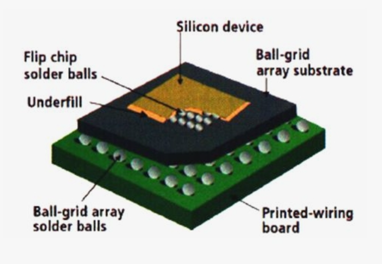
BGA Package Cross Section
Understanding the BGA package cross section helps explain both electrical behavior and assembly challenges. Typical bga package cross section layers including:
- Silicon Die – The actual integrated circuit
- Die Attach Material – Bonds the die to the substrate
- Substrate (BT resin, ABF, etc.) – Routes signals from die to solder balls
- Bond Wires or Flip-Chip Bumps – Electrical connection between die and substrate
- Solder Mask Layer – Defines pad openings
- Solder Balls – External connections to PCB
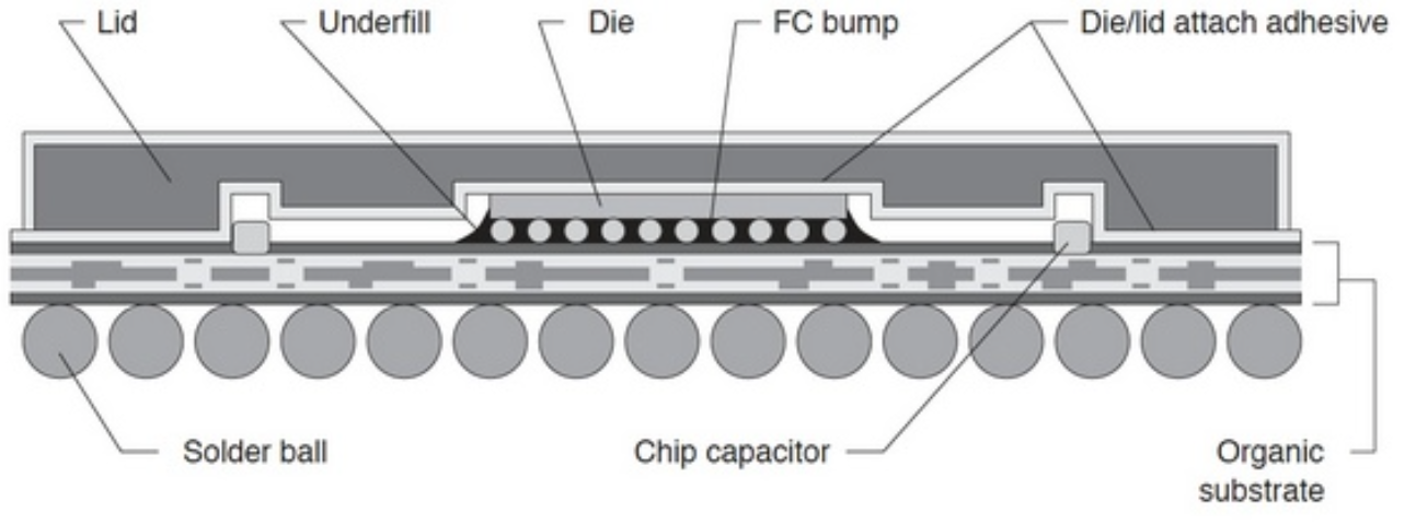
In a typical cross-section:
- The silicon die is mounted on a substrate.
- Wire bonds or flip-chip bumps connect the die to the substrate.
- The organic substrate redistributes signals to the solder balls.
- Solder balls form the interface between package and PCB pads.
This layered structure supports high signal density while isolating mechanical stress between silicon and PCB materials.
What Are the Different Types of BGA?
Ball Grid Array (BGA) is not a single package format but a family of package structures optimized for different electrical, thermal, mechanical, and cost requirements. Understanding the different BGA type package variants is critical for PCB layout, stack-up planning, assembly process selection, and long-term reliability control. Common BGA type package families include:
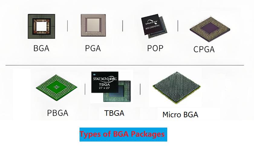
1. PBGA (Plastic Ball Grid Array)
PBGA uses an organic substrate with a wire-bonded die and plastic encapsulation. Typical ball pitch ranges from 1.27 mm to 0.65 mm, with ball counts commonly between 100 and 900 I/Os. It is the most widely adopted BGA package in high-volume electronics.
Advantages
- Low cost and mature supply chain
- Compatible with standard SMT processes
- Good balance of performance and manufacturability
2. CBGA (Ceramic Ball Grid Array)
CBGA is built on a multilayer ceramic substrate, offering higher thermal conductivity than organic materials. Ball pitch is usually 1.27 mm or larger, and package sizes often exceed 20 × 20 mm. It is designed for long-term reliability under thermal stress.
Advantages
- Excellent thermal stability
- Minimal warpage across temperature cycles
- Suitable for high-reliability applications
3. FBGA (Fine-Pitch Ball Grid Array)
FBGA is a compact BGA variant with reduced ball pitch, typically 0.8 mm, 0.65 mm, or 0.5 mm. It enables higher I/O density within a smaller footprint while maintaining acceptable electrical performance.
Advantages
- Smaller package size
- Higher routing density
- Well suited for HDI PCB designs
4. FCBGA (Flip-Chip Ball Grid Array)
In FCBGA, the silicon die is mounted face-down and connected to the substrate using micro bumps. This structure supports very high I/O counts (1,000+ balls) and excellent thermal paths from die to PCB.
Advantages
- Superior high-speed signal performance
- Excellent heat dissipation
- Ideal for high-power and high-frequency devices
5. TBGA (Tape Ball Grid Array)
TBGA uses a flexible polyimide tape as the substrate, resulting in a thinner and lighter package. Ball pitch typically ranges from 0.8 mm to 1.27 mm, with moderate I/O density.
Advantages
- Thin and lightweight structure
- Reduced mechanical stress
- Suitable for space-limited designs
6. PoP BGA (Package on Package)
PoP integrates two BGA packages stacked vertically, commonly logic on the bottom and memory on top. It reduces PCB area while maintaining short interconnect lengths between stacked components.
Advantages
- Significant PCB space savings
- Improved signal integrity between logic and memory
- Flexible memory configuration
7. Micro BGA (µBGA)
Micro BGA refers to ultra-small BGAs with ball pitch typically ≤0.5 mm and very compact outlines. These packages are optimized for extreme miniaturization and high-density interconnections.
Advantages
- Maximum size reduction
- High electrical performance in small form factors
- Ideal for advanced HDI and microvia PCBs
Each type places different demands on PCB stack-up design, solder mask strategy, and assembly process control.
How Does BGA Compare to Other Packages?
When compared with QFP, SOP, or QFN packages, BGAs offer a clear advantage in I/O scalability and signal performance.
| Feature | BGA | QFP | QFN | LGA |
| I/O Density | Very high | Medium | Medium | High |
| Footprint | Small | Large | Small | Small |
| Routing Complexity | High | Low | Medium | High |
| Assembly Difficulty | High | Low | Medium | Medium |
| Reworkability | Difficult | Easy | Medium | Medium |
However, BGAs require more advanced PCB fabrication and assembly capabilities, particularly for inspection, rework, and thermal profiling.
What Is the Difference Between LGA and BGA Packaging?
The key distinction lies in how the electrical connection is formed.
- BGA: Uses solder balls attached to the package; soldering occurs during PCB assembly.
- LGA: Uses flat pads on the package; solder or contact springs are on the PCB side.
BGA packages generally offer stronger mechanical joints after reflow, while LGA packaging can simplify rework and reduce package height in some applications.
Is BGA Used in Mobile Phones?
Yes. BGA and its derivatives are extensively used in smartphones and mobile devices.
Typical mobile BGA applications include:
- Application processors
- Memory devices (eMMC, LPDDR)
- RF baseband and connectivity chips
Ultra-fine pitch BGAs and PoP structures are especially common, supporting compact layouts while maintaining high data throughput.
Common Uses of BGA Package
The bga type package is found across a wide range of industries and applications, including:
- Consumer electronics and smart devices
- Networking and data communication equipment
- Industrial control systems
- Automotive electronics
- Medical and diagnostic equipment
- High-performance computing and servers
As PCB designs continue to push toward higher speed, smaller size, and greater integration, BGA packaging remains one of the most adaptable and future-proof interconnection solutions.
Why BGA Expertise Matters in PCB Assembly?
Not all PCBA manufacturers are equal when it comes to BGA. Fine-pitch BGA, microBGA, and flip-chip BGA require advanced capability, experience, and strict process control.
Our BGA Assembly Capabilities Include:
- 0.4 mm / 0.5 mm fine-pitch BGA assembly
- HDI PCB manufacturing with microvias & via-in-pad
- Advanced X-ray inspection for 100% BGA verification
- Precise reflow profile control
- BGA rework and repair services
- DFM analysis to reduce risk and cost
- IPC Class 2 & Class 3 assembly support
Why Choose Us for BGA PCB Assembly?
With years of experience in high-density and high-reliability electronics, we support customers across consumer, industrial, automotive, and medical sectors.
We provide:
- One-stop PCB fabrication + assembly
- Dedicated engineering support
- Strict quality control and traceability
- Competitive pricing with no compromise on reliability
- Fast turnaround for prototypes and volume production
Looking for a reliable partner experienced in all BGA type packages?
Contact us today for a free DFM review and professional support on your next BGA PCB project.
FAQ
1. Are BGA packages hard to repair?
Yes. BGA rework requires specialized equipment and skilled technicians.
2. What is the smallest BGA package size?
microBGA and WLCSP packages can be under 3 × 3 mm.
3. Can BGA be hand-soldered?
No. BGA packages require reflow soldering.
4. Is BGA more reliable than QFN?
For high pin count and high-speed applications, yes—when properly designed and assembled.