

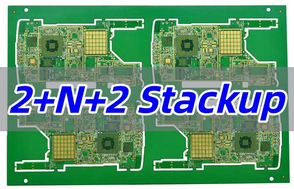
A 2+N+2 stackup is a specific high-density interconnect (HDI) printed circuit board configuration, characterized by two sequential lamination cycles building up HDI layers on either side of a core. This architecture is fundamental for creating the dense, reliable, and high-performance interconnections required in modern electronics. This article will explore the structure, benefits, and design considerations of the 2+N+2 stackup, explaining why it is often the ideal choice for complex HDI PCB manufacturing.
Are you struggling to pack more functionality into a smaller PCB footprint while maintaining signal integrity and reliability? As devices shrink and performance demands soar, standard PCB constructions often hit a wall. Designers frequently encounter:
- Signal Integrity Issues: Increased crosstalk and impedance discontinuities in complex, dense layouts.
- Limited Routing Density: Inability to escape from fine-pitch BGAs and other advanced components with standard through-hole vias.
- Manufacturing Complexity and Cost: Difficulty balancing the performance needs of HDI with a cost-effective and reliable fabrication process.
- Reliability Concerns: Weak points in the via structure, especially when connecting multiple layers, leading to potential failures.
- Thermal Management Challenges: Effectively dissipating heat in a compact, multi-layer board.
Fortunately, the 2+N+2 stackup directly addresses these challenges. This HDI approach provides a structured path to higher performance without compromising on manufacturability. The key solutions it offers include:
- Superior Signal Integrity: Controlled impedance and reduced crosstalk through well-defined microvia structures and optimized dielectric spacing.
- Maximum Routing Density: Efficient component escape routing using stacked or staggered microvias, enabling HDI 1+n+1 and beyond.
- Optimized Manufacturing Flow: A balanced structure that leverages proven sequential lamination cycles, improving yield and controlling costs.
- Enhanced Reliability: Robust interconnects with stacked or staggered vias that are more reliable than complex through-hole via structures in thin boards.
- Effective Thermal and Power Distribution: A dedicated core section (
N) for solid power and ground planes, improving heat spreading and PDN stability.
At BEST Technology, we specialize in advanced PCB manufacturing, with deep expertise in HDI and complex stackups like 2+N+2. Our engineering support team can help you optimize your design for performance, reliability, and cost-effectiveness, ensuring your product succeeds in a competitive market. For inquiries, please contact us at sales@bestpcbs.com.
What is 2+N+2 Stackup?
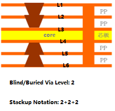
In essence, a 2+N+2 stackup describes the layer build-up of an HDI PCB. The notation breaks down as follows:
- The first and last “2” represent two HDI layers built sequentially on the top and bottom of the board. These layers typically use microvias (laser-drilled) for interconnection.
- The “N” represents the internal core, which can be any even number of layers (e.g., 2, 4, 6). This core is manufactured separately and contains standard mechanically drilled plated through holes (PTHs).
This structure requires two separate lamination cycles: first to create the core, and second to laminate the top and bottom HDI buildup layers onto it. This is a step beyond a simpler HDI 1+n+1 stackup, offering greater routing density and design flexibility.
As shown in the photo below:
- L1 build-up
- L2 build-up
- L3 core
- L4 core
- L5 build-up
- L6 build-up
What is a Typical PCB Stackup?
A typical PCB stackup refers to the arrangement of copper and insulating layers that make up a circuit board. Its primary functions are to:
- Control Impedance: Precise dielectric thicknesses and trace widths are used to achieve target impedance values (e.g., 50Ω single-ended, 100Ω differential), which is crucial for signal integrity. Using a PCB stackup impedance calculator is essential during design.
- Provide Shielding: Ground planes are strategically placed to shield sensitive signals from noise.
- Manage Heat and Power: Dedicated planes distribute power and help dissipate heat.
A standard stackup might be simple, like a 2-layer board, or complex, like the 2 n 2 stackup HDI used for advanced applications. The choice depends entirely on the circuit’s complexity and performance requirements.
What is a 2 Layer PCB Structure?
A 2-layer PCB, the simplest multilayer structure, is defined by the following key characteristics:
- Layer Structure: It is composed of three fundamental elements:
- A top copper layer for components and traces.
- A dielectric substrate core (e.g., FR-4) in the middle.
- A bottom copper layer for components and traces.
- Key Features:
- Components and routing traces can be placed on both the top and bottom sides of the board.
- Electrical connections between the two layers are made exclusively using plated through-hole (PTH) vias, which are holes drilled through the entire board and plated with copper.
What is the Standard 1.6 mm 2 Layer Stackup?
A common standard for a 2-layer PCB is a 1.6mm overall thickness. A typical build-up might be:
- Top Layer: 1 oz (35µm / 0.035mm) Copper
- Dielectric Core: ~1.5mm (e.g., FR-4)
- Bottom Layer: 1 oz (35µm / 0.035mm) Copper
This simple structure is cost-effective but offers limited routing space and cannot support the high-speed or dense designs that necessitate an advanced circuits stackup like 2+N+2.
What are the Standard HDI Stackups?
HDI stackups are classified by the number of sequential laminations and the via structures used. The most common standard HDI stackups are:
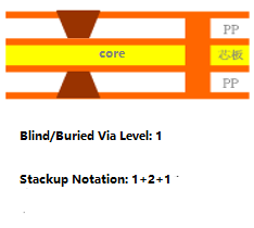
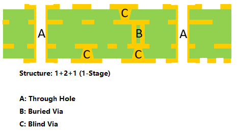
1+N+1: This is the simplest HDI type, featuring one HDI buildup layer on each side of the core. It primarily uses microvias to connect the surface layer directly to the first inner layer.
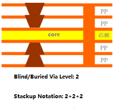
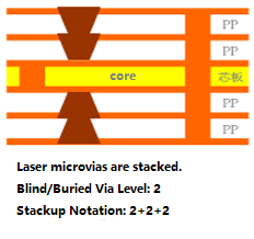
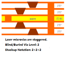
2+N+2: This stackup features two HDI buildup layers on each side of the core. This allows for more complex routing and a higher density of components. The microvias can be implemented in either a stacked or staggered configuration.
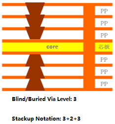
3+N+3 and Beyond: Used for extremely complex designs, these stackups require three or more sequential lamination cycles. They offer the highest possible density and component integration but at a significantly greater cost.
What is the Difference between Stacked and Staggered Via?
In a 2 n 2 stackup HDI PCB, microvias connecting different layers can be arranged in two primary ways:
- Stacked Vias: Microvias are placed directly on top of one another, creating a continuous vertical connection through multiple HDI layers. This saves horizontal space but can be more challenging to manufacture reliably due to potential voiding in the fill material.
- Staggered Vias: Microvias are offset from one another, connecting adjacent layers in a step-like pattern. This is often more reliable from a manufacturing standpoint but consumes more routing area on the inner layers.
The choice between stacked vs. staggered depends on density requirements, manufacturer capability, and reliability specifications.
What is V in PCB Board?
In the context of vias, “V” simply stands for “Via.” A via is a plated hole that provides an electrical connection between different layers of a PCB. In HDI discussions, you’ll encounter terms like:
- Microvia: A small via (typically <0.15mm diameter) laser-drilled, used in HDI layers.
- Through-Hole Via: A via that passes through the entire board.
- Blind Via: Connects an outer layer to an inner layer without going through the entire board.
- Buried Via: Connects inner layers only and is not visible on the surface.
How Much Current can a 0.2 mm Trace Carry?
The current-carrying capacity (ampacity) of a PCB trace mainly depends on its cross-sectional area (trace width × copper thickness) and how well the board dissipates heat. External traces carry more current than internal traces because they cool more efficiently.
For a 0.2 mm (≈8 mil) wide, 1 oz (≈35 µm) external copper trace on FR-4, a practical estimate for a 10°C temperature rise is around 1.0 A.
Below is a simplified calculation using clear text (no formulas that will break when pasted).
1. Define the trace geometry
- Trace width: 0.2 mm ≈ 8 mil
- Copper thickness (1 oz): 35 µm ≈ 1.37 mil
2. Calculate the cross-sectional area
Area = width (mil) × thickness (mil)
- Area ≈ 8 mil × 1.37 mil
- Result ≈ 11 mil²
3. Apply the IPC-2221 external-trace approximation
IPC-2221 uses an empirical relationship between:
- current
- trace area
- temperature rise
Using the simplified IPC-2221 external-layer approximation:
- At ΔT ≈ 10°C
- Area ≈ 11 mil²
- Copper thickness = 1 oz
The resulting ampacity is roughly 0.7–0.8 A.
4. Compare with IPC-2152 (newer standard)
IPC-2152 generally gives slightly higher allowable currents for the same conditions.
For a 0.2 mm (8 mil) external trace at 1 oz copper and 10°C rise:
- IPC-2152 calculators usually give 0.8–1.0 A
⭐ Practical design value
To keep it simple and safe:
A 0.2 mm external trace with 1 oz copper can typically carry about 1 A for a small temperature rise.
✔ Design Recommendations
1. Always confirm with an IPC-2152-based trace-width calculator
This is essential for power nets.
2. Consider environment and board conditions
- Higher ambient temperature reduces ampacity
- Inner layers can carry less current
- Thicker copper increases ampacity
3. Add margin for reliability
Even if the estimate suggests 1 A, many engineers will design it for 0.7–0.8 A continuous to improve safety and lifetime.
4. Separate power nets from small-signal nets
High-current rules matter only for power distribution, not for tiny loads (like a 2N2222 transistor’s base current).
How to Reduce Crosstalk in PCB?
Crosstalk is unwanted coupling of energy between adjacent signals. In dense 2 n 2 stackup PCB designs, reducing it is critical. Key methods include:
- Increase Spacing: The most effective method; follow the 3W rule (center-to-center spacing should be at least 3x the trace width).
- Use Guard Traces: Placing grounded traces between sensitive lines can isolate them.
- Maintain a Continuous Reference Plane: Signals routed over a solid ground plane experience far less crosstalk than those crossing plane splits.
- Minimize Parallel Run Length: Keep the length that signals run parallel to each other as short as possible.
- Controlled Impedance: Proper stackup design with controlled dielectric heights helps manage electric fields.
Why Choose EBest Circuit (Best Technology) for 2 N 2 Stackup HDI PCB Manufacturing?
Selecting the right manufacturing partner is critical for the success of complex HDI boards. BEST Technology offers distinct advantages for your 2+N+2 stackup projects:
- Advanced Process Capability: We possess state-of-the-art laser drilling and lamination equipment necessary for reliable microvia formation, whether stacked or staggered.
- Expert Engineering Support: Our team provides PCB stackup impedance calculator guidance and design-for-manufacturability (DFM) reviews to optimize your layout for performance and yield.
- Proven Quality and Reliability: We adhere to strict quality standards, ensuring the reliability of every via structure and layer-to-layer registration in your HDI printed circuit board.
- Material Expertise: We can recommend the optimal materials, from standard FR-4 to high-speed/low-loss laminates, to meet your electrical and thermal requirements.
In summary, the 2+N+2 stackup is a powerful HDI PCB architecture that provides the ideal balance of high routing density, superior signal integrity, and reliable manufacturability for today’s advanced electronic products. This article has detailed the structure, benefits, and key design considerations of the 2+N+2 stackup, demonstrating why it is a preferred choice for complex designs. For your next HDI project, partner with a HDI PCB manufacturer that has the expertise to bring your design to life reliably and efficiently. Trust BEST Technology to deliver high-quality 2 n 2 stackup HDI PCBs. A warm welcome to contact our team at sales@bestpcbs.com to discuss your requirements.
FAQs about 2+N+2 Stackup
1. How do you define the via steps for laser-drilled blind vias?
For laser blind vias, the step count is based on the build-up layers in the HDI stack-up.
- Each additional build-up layer corresponds to one laser via step.
- Example: A 1+N+1 structure is typically a 1-step HDI; a 2+N+2 structure is usually 2-step.
2. How do you define the via steps for mechanically drilled blind/buried vias?
Mechanical drilling follows a different logic. The step count depends on the number of drilling cycles required.
- If the hole can be drilled in one cycle, it is considered 1-step.
- If it must be drilled twice, it counts as 2-step.
- More drilling cycles = higher step count.
3. Why is step counting different for laser vs mechanical drilling?
- Laser vias are tied to HDI build-up technology, so the step count follows the build-up sequence.
- Mechanical drilling spans deeper layers and larger holes, so its step count is determined by how many drilling operations are required to complete the via structure.
4. How do you determine the step count when both laser and mechanical vias are used?
Engineers evaluate:
- The full stack-up,
- Which layers use laser vs mechanical drilling,
- The process order.
Laser vias are counted according to build-up layers, while mechanical vias follow drilling cycles. Both are combined to identify the overall HDI step level.
5. Does a higher step count increase manufacturing cost?
Yes.
More steps mean more lamination, drilling, and processing cycles. Costs can increase sharply:
- 1-step HDI adds roughly 20–30% to cost.
- 2-step HDI can be significantly higher, sometimes close to double, depending on factory capability.