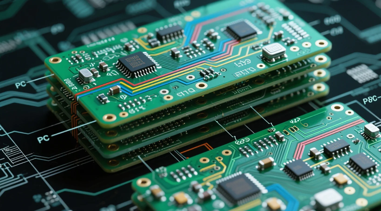
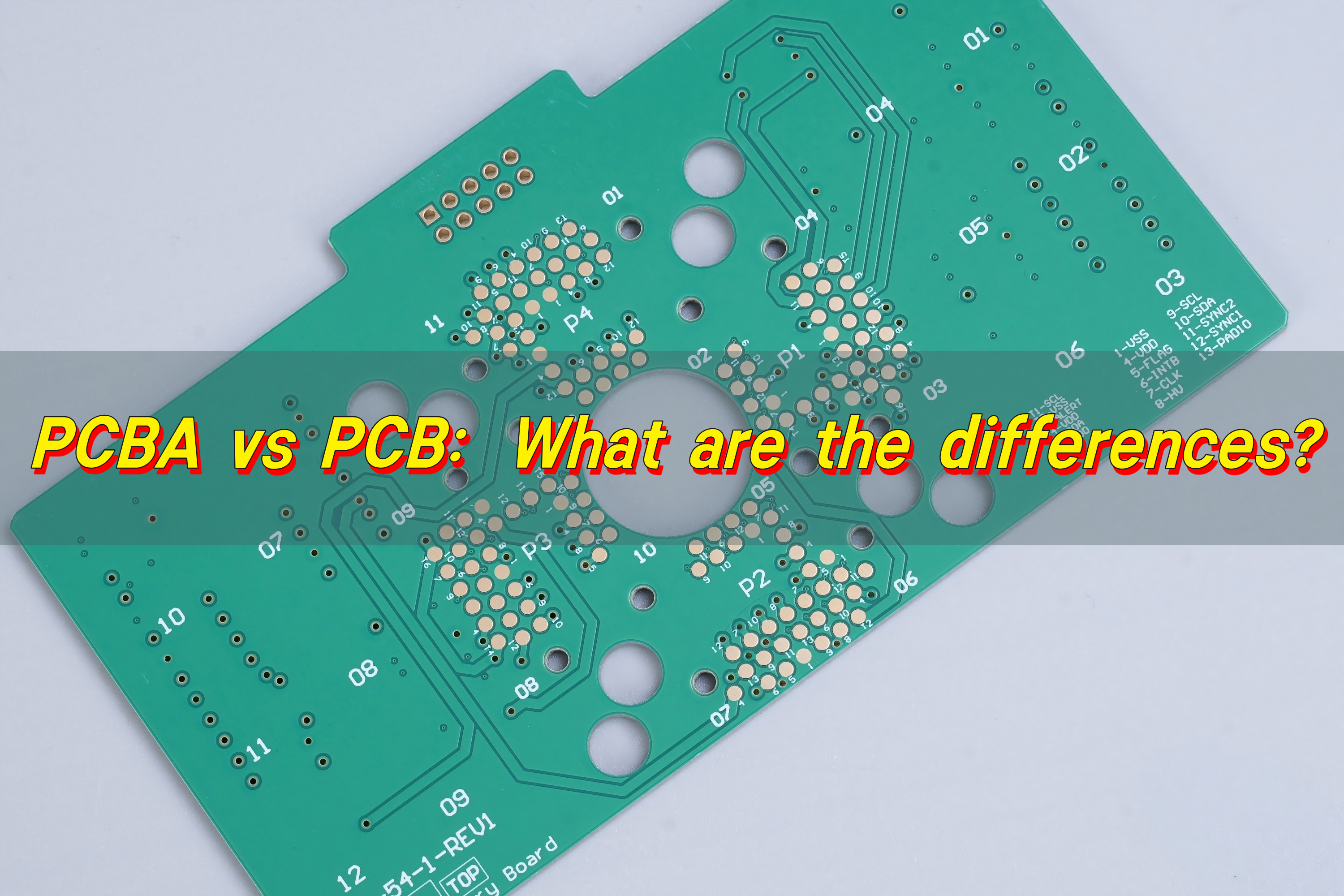
Looking for reliable PCB manufacturer in Kenya? This blog is mainly about challenges and solutions of Kenya PCB Manufacturer and why choose EBest Circuit (Best Technology) for your project.
Kenya’s thriving electronics sector, fueled by demand for smart agricultural sensors, affordable consumer electronics, and renewable energy equipment, is driving rapid growth in the local circuit board industry. With more and more local startups and international companies launching electronics projects in Kenya, the need for reliable, high-quality PCB solutions is more critical than ever. This is where EBest Circuit (Best Technology) stands out as a trusted PCB manufacturer in Kenya: with decades of experience providing customized, high-quality PCB solutions to the global market, we are perfectly positioned to meet the unique needs of Kenyan electronics businesses. Whether providing rapid prototyping services for IoT startups in Nairobi or large-scale production for industrial control systems, we have become a reliable partner, helping local businesses overcome industry challenges and ensure project success.
Top PCB Manufacturer in Kenya
| Company Name | Main Business | Core Advantages | Process Capability | Lead Time |
| EBest Circuit (Best Technology) Co.,Ltd | Custom PCB manufacturing, PCB prototyping, multi-layer PCB production, PCB assembly supporting services | International quality certification, global supply chain support, 24/7 technical service, no minimum order quantity restriction | 1-40 layers PCB, 3mil/3mil line width/spacing, 0.1mm laser drilling, HDI/flexible/rigid-flex PCB support | Prototyping: 24-48h (expedited)/3-5 day (standard); Mass production: 5-10 day (standard)/7-15 day (complex) |
| Webwave Electric Manufacturing (K) Co.,Ltd | Single/double-layer PCB manufacturing, industrial control PCB production, PCB maintenance | Familiar with local industrial standards, flexible payment terms, on-site technical guidance | 1-2 layers PCB, 8mil/8mil line width/spacing, 1-2oz copper thickness, simple hole processing | Prototyping: 7-10 day; Mass production: 12-20 day |
| Power Controls Ltd | Control system PCB manufacturing, PCB testing services, electronic control component matching | Strong control system professional matching ability, reliable quality testing, long-term cooperation with local electrical enterprises | 1-4 layers PCB, 7mil/7mil line width/spacing, ±10% impedance control, standard surface treatment | Prototyping: 6-8 day; Mass production: 11-18 day |
| Synkron International | Small-batch PCB prototyping, custom PCB for IoT devices, PCB design supporting | Focus on emerging electronic fields, close cooperation with local tech startups, flexible customization | 1-4 layers PCB, 5mil/5mil line width/spacing, FR-4/flexible material support, simple HDI processing | Prototyping: 4-6 day; Mass production: 9-14 day |
| HISTOTO Limited | Industrial PCB manufacturing, high-temperature PCB production, PCB maintenance and renovation | Rich experience in industrial field, strong environmental adaptability of products, professional after-sales team | 1-4 layers PCB, 6mil/6mil line width/spacing, high-temperature/thick copper material support | Prototyping: 8-10 day; Mass production: 14-21 day |
| Jong Indu General Contractors | PCB manufacturing for construction electrical systems, custom large-size PCB, supporting installation services | Integration of production and installation, familiar with construction industry norms, large-size product processing capacity | 1-3 layers PCB, max 600mm×1200mm size, 10mil/10mil line width/spacing, standard surface treatment | Prototyping: 10-14 day; Mass production: 18-25 day |
| Cloud On Earth HVAC & R Limited | PCB for HVAC control systems, custom electronic control board production, PCB testing | Professional matching for HVAC industry, stable product performance, on-time delivery guarantee | 1-4 layers PCB, 7mil/7mil line width/spacing, moisture-proof surface treatment, impedance control | Prototyping: 6-9 day; Mass production: 12-17 day |
Challenges of PCB Manufacturer in Kenya
- Unstable supply of raw materials, high dependence on imports, leading to frequent delays in production scheduling due to material shortages.
- Insufficient precision of production equipment, difficulty in meeting the processing requirements of high-density, multi-layer PCB products.
- Long lead times for prototyping and mass production, unable to keep up with the progress of urgent electronic projects.
- Inconsistent product quality, frequent occurrence of problems such as line oxidation, poor conduction, and solder pad deviation.
- High production and material costs, limited pricing competitiveness due to small production scale and high import logistics costs.
- Lack of professional technical support, unable to provide effective solutions for custom PCB design and process optimization.
- Unreliable energy supply and inadequate infrastructure, which affect the stability of continuous production and product yield.
- Difficulty in complying with international environmental and quality standards, restricting the export of products to regional and global markets.
Our Solutions to These Challenges
- Stable Global Supply Chain Support: To address the instability of raw material supply and heavy reliance on imports in Kenya, EBest Circuit (Best Technology) has established long-term partnerships with renowned raw material suppliers such as Shengyi Technology. We maintain a 30-day safety stock of commonly used materials to ensure a stable supply for all PCB projects in Kenya, preventing production delays due to material shortages.
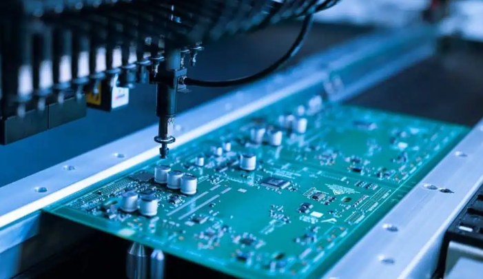
- Cutting-Edge Equipment for High-Precision Requirements: We are equipped with advanced equipment such as high-precision exposure machines and AOI automatic optical inspection systems, with laser drilling accuracy less than 0.1mm. This enables us to produce 1-40 layer HDI boards, fully meeting the processing requirements for high-density, multi-layer PCB products in Kenya’s rapidly developing electronics industry.
- Efficient Production to Meet Tight Deadlines: Our optimized production management system ensures fast turnaround times – 24-48 hours for expedited prototypes and 3-5 days for standard prototypes. The standard lead time for mass production is 5-10 days. We also reserve 15% of our capacity specifically for urgent orders, ensuring your projects stay on schedule.
- Rigorous Quality Control for Product Reliability: EBest Circuit (Best Technology) is ISO 9001 certified. We implement full-process quality inspection from raw material warehousing to finished product delivery, strictly controlling key indicators such as line width tolerance (±10%) and solder mask alignment accuracy (≤50μm). Each batch of products comes with a detailed quality traceability report, giving you peace of mind.
- Cost-Optimized Solutions Tailored for Kenya: Leveraging our large-scale production advantages, we reduce unit costs without compromising quality. We also provide customized logistics solutions for Kenya, including multimodal transportation and tax optimization, reducing import logistics costs by 15-20% compared to local Kenyan manufacturers.
- 24/7 Dedicated Technical Support for Kenya: We have established a dedicated technical team to serve Kenyan customers, providing one-on-one solutions for customized PCB design, process optimization, and other related issues. Our average response time for inquiries is within 2 hours, ensuring timely resolution of technical problems throughout your project.
- Reliable Production Stability: Our production system is unaffected by Kenya’s unstable energy supply and inadequate infrastructure. We maintain a product yield rate of over 99.5%, ensuring consistent and reliable delivery of your orders.
- Meeting international standards and facilitating global expansion: All our products fully comply with RoHS 2.0 and REACH regulations, and we provide official certification documents. This helps our Kenyan customers successfully enter regional and global markets to expand their business scope.
Why Kenya Clients Choose EBest Circuit (Best Technology) for PCB Manufacturer?
Reasons Why Kenya Clients Choose EBest Circuit (Best Technology) for PCB Manufacturer:
- 19 Years of Industry Expertise Driving Cost Efficiency: Decades of experience enable precise prediction of cost loss points in design and production, optimizing schemes in advance to shorten R&D cycles by 20% and reduce time-related costs.
- Free DFM Analysis Service: Professional Design for Manufacturability analysis provides optimization feedback within 2 hours, reducing design iterations and prototype failure rates to enhance R&D efficiency.
- Comprehensive Certifications for Diverse Industries: Holding ISO 9001, IATF 16949 automotive electronics, medical-grade production, and RoHS certifications to meet compliance needs in industrial, medical, automotive, and other high-end sectors.
- Competitive Pricing Strategy for Cost-Sensitive Needs: Leveraging large-scale production advantages, our PCB products are priced 10-15% below Kenya’s local average while maintaining premium raw material quality, significantly reducing overall project procurement costs.
- 24-Hour Rapid Prototyping Service: Emergency orders achieve 24-hour delivery for single/double-layer PCB prototypes and 48-hour delivery for 8-layer or fewer multilayer boards, addressing urgent R&D iteration timelines.
- Customized Cost-Sensitive Design Solutions: Tailor material substitution and process optimization recommendations to project budgets, helping clients reduce production costs by 15-20% on average and eliminate wasteful over-design.
- Guaranteed On-Time Delivery with 99.2% Accuracy: Standard batch production lead times of 5-10 days and complex multilayer boards within 7-15 days ensure 99.2% of orders are delivered as scheduled, preventing project delays.
- 100% Batch Inspection Coverage for Zero Quality Concerns: All batch orders undergo dual AOI automatic optical inspection and manual verification, maintaining a 99.8%+ pass rate to minimize rework costs from defects.
- End-to-End Strict Quality Control: Full-cycle systems cover incoming raw material checks, in-process controls, and outgoing product testing with ±10% tolerance on critical parameters for performance consistency.
Our PCB Prototyping Service
EBest Circuit (Best Technology)’s PCB prototyping service for Kenya provides a comprehensive range of options to address diverse project requirements. This includes single-layer, double-layer, multi-layer (1-40 layers), flexible, rigid-flex, and HDI PCBs. Material customization is supported, featuring FR-4, aluminum substrates, and high-temperature resistant materials tailored to industrial control, IoT, consumer electronics, and other application-specific needs.
The service eliminates minimum order constraints, accommodating quantities as small as one unit. This flexibility is ideal for small-batch R&D and trial production projects, reducing unnecessary cost burdens while supporting agile development cycles.
Surface treatments are customizable to meet environmental adaptability and reliability standards, with options like lead-free tin, immersion gold, and OSP. Each completed prototype is accompanied by a detailed test report that covers critical parameters including impedance, continuity, insulation, and other key indicators, ensuring full alignment with design specifications and performance expectations.
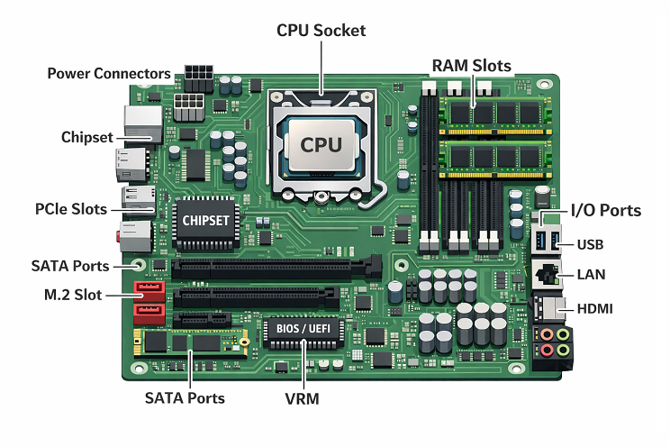
Our PCB Manufacturing Capabilities
| Item | Capabilities |
| Layer Count | 1 – 32 Layers |
| Max Board Dimension | 2424″ (610610mm) |
| Min Board Thickness | 0.15mm |
| Max Board Thickness | 6.0mm – 8.0mm |
| Copper Thickness | Outer Layer: 1oz~30oz, Inner Layer: 0.5oz~30oz |
| Min Line Width/Line Space | Normal: 4/4mil (0.10mm); HDI: 3/3mil (0.076mm) |
| Min Hole Diameter | Normal: 8mil (0.20mm); HDI: 4mil (0.10mm) |
| Min Punch Hole Dia | 0.1″ (2.5mm) |
| Min Hole Spacing | 12mil (0.3mm) |
| Min PAD Ring(Single) | 3mil (0.075mm) |
| PTH Wall Thickness | Normal: 0.59mil (15um); HDI: 0.48mil (12um) |
| Min Solder PAD Dia | Normal: 14mil (0.35mm); HDI: 10mil (0.25mm) |
| Min Soldermask Bridge | Normal: 8mil (0.2mm); HDI: 6mil (0.15mm) |
| Min BAG PAD Margin | 5mil (0.125mm) |
| PTH/NPTH Dia Tolerance | PTH: ±3mil (0.075mm); NPTH: ±2mil (0.05mm) |
| Hole Position Deviation | ±2mil (0.05mm) |
| Outline Tolerance | CNC: ±6mil (0.15mm); Die Punch: ±4mil (0.1mm); Precision Die: ±2mil (0.05mm) |
| Impedance Controlled | Value>50ohm: ±10%; Value≤50ohm: ±5ohm |
| Max Aspect Ratio | 0.334027778 |
| Surface Treatment | ENIG, Flash Gold, Hard Gold Finger, Gold Plating(50mil), Gold finger, Selected Gold plating, ENEPIG, ENIPIG; HAL, HASL(LF), OSP, Silver Immersion, Tin Immersion |
| Soldermask Color | Green/White/Black/Yellow/Blue/Red |
Our Lead Time for Kenya PCB Prototyping
| Layers | Normal Service | Fastest Service |
| 1 | 7 Days | 24 H |
| 2 | 8 Days | 24 H |
| 4 | 10 Days | 48 H |
| 6 | 10 Days | 72 H |
| 8 | 12 Days | 72 H |
| ≥10 | TBD | TBD |
Case Studies of Our Kenya PCB Manufacturing
Project Background
A Nairobi-based industrial automation company required rapid development of a high-reliability control module for smart factory equipment. The project demanded multi-layer (8-layer) PCBs with strict impedance control, high-temperature resistance, and compliance with industrial IoT standards. Key constraints included a tight 6-week R&D timeline and a 15% cost reduction target compared to local competitors.
Project Challenges
- Time Sensitivity: Design validation required 3 prototype iterations within 3 weeks.
- Technical Complexity: 8-layer HDI design with 0.1mm line/space and buried vias for compact form factor.
- Cost Pressure: Budget constraints necessitated material substitution (e.g., FR-4 to high-Tg FR-4) without compromising thermal performance.
- Quality Compliance: Must meet ISO 9001 and IATF 16949 standards for industrial control applications.
Our Solution
- Rapid Prototyping: Leveraged 48-hour 8-layer PCB prototyping to compress design validation cycles. Free DFM analysis identified 12 design optimization points (e.g., hole size adjustment, solder mask alignment), reducing first-article failure risk by 40%.
- Material Customization: Engineered high-Tg FR-4 substrate with aluminum heat sink integration, balancing cost savings and thermal performance. Surface treatments included ENIG for corrosion resistance.
- Process Optimization: Applied blind via drilling and impedance control techniques to meet signal integrity requirements. AOI + X-ray inspection ensured 100% defect detection.
- Pricing Strategy: Scaled production enabled 12% cost reduction versus local averages while maintaining premium raw material sourcing.
Project Outcomes
- Timeline Achievement: Full prototype validation completed in 18 days (vs. 21-day target), enabling 2-week early market launch.
- Cost Efficiency: 18% overall cost savings achieved through material optimization and process streamlining.
- Quality Excellence: 99.7% first-pass yield with zero field failures reported over 12-month deployment.
- Certification Compliance: Full adherence to ISO 9001 and IATF 16949 standards, validated by third-party audits.
How to Get A Quote for Your PCB Project?
8 Steps to Get A Quote for Your PCB Project:
1. Submit Your Project Requirements Clearly
- Provide detailed specifications of your PCB project, including dimensions, layer count, copper thickness, and required materials (e.g., FR-4, aluminum).
- Include technical drawings, Gerber files, or BOM (Bill of Materials) for accurate quoting.
- Specify any certifications needed (e.g., RoHS, ISO) and compliance with Kenyan regulatory standards.
2. Choose Suitable Material and Surface Finish
- Select materials based on your project’s application (e.g., high-frequency PCBs may require Rogers or Teflon).
- Decide on surface finishes like HASL, ENIG, or OSP, considering cost, conductivity, and environmental factors relevant to Kenya’s climate.
3. Define Quantity and Production Timeline
- Share your target order quantity (e.g., prototype, small batch, or bulk). Volume affects per-unit pricing.
- Indicate deadlines for prototyping, sample approval, and mass production. Lead times may vary based on complexity and logistics.
4. Clarify Packaging and Shipping Preferences
- Specify packaging requirements (e.g., anti-static bags, bulk boxes) to protect PCBs during transit to Kenya.
- Discuss shipping methods (air, sea, or express) and include port/destination details (e.g., Mombasa, Nairobi). Factor in local customs clearance and import duties.
5. Request Transparent Pricing Breakdown
- Ask for a detailed quote separating costs for materials, fabrication, assembly, testing, and shipping.
- Ensure pricing includes all taxes, tariffs, and fees applicable to Kenyan imports. Confirm payment terms (e.g., T/T, LC, or local currency options like KES).
6. Engage in Pre-Production Communication
- Collaborate with the supplier to address potential design or manufacturing challenges early.
- Confirm sample approval processes and quality control measures (e.g., visual inspection, AOI, or X-ray testing).
7. Leverage Local Partnerships or Agents
- Consider working with Kenyan-based agents or logistics partners to streamline communication, reduce costs, and ensure compliance with local business practices.
8. Review Terms and Conditions Thoroughly
- Evaluate warranty policies, after-sales support, and liability clauses.
- Ensure agreements align with Kenyan contract law and international trade regulations.
Welcome to contact us if you have any request for PCB design, prototyping, production and assembly: sales@bestpcbs.com.