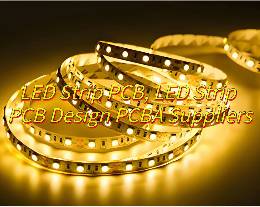
Why choose LED strip black PCB for professional lighting projects? This guide covers materials, thermal management, waterproofing, testing, and customization options for optimal performance.
EBest Circuit (Best Technology) excels in delivering high-quality waterproof LED strip black PCB with industry-leading advantages. Our production efficiency ensures fast lead times, with standard orders shipped within 7–10 days, reducing downtime for clients. The waterproof performance is unmatched, utilizing dual-layer silicone encapsulation and precision sealing to achieve IP67–IP68 ratings, ideal for outdoor, marine, and high-moisture environments. Customization options include adjustable LED density (30–144 LEDs/m), color temperatures (2700K–6500K), and compatibility with SPI/DMX controls. Rigorous quality testing guarantees longevity, while competitive pricing and responsive support make us a preferred partner for architects, engineers, and lighting designers. Welcome to contact us if you have any request for LED strip black PCB: sales@bestpcbs.com.
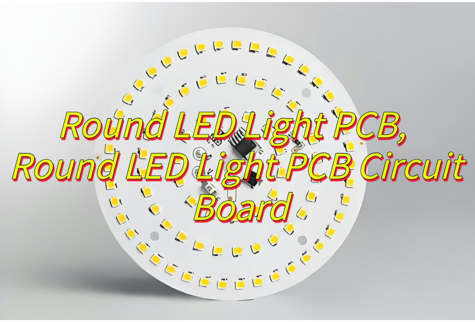
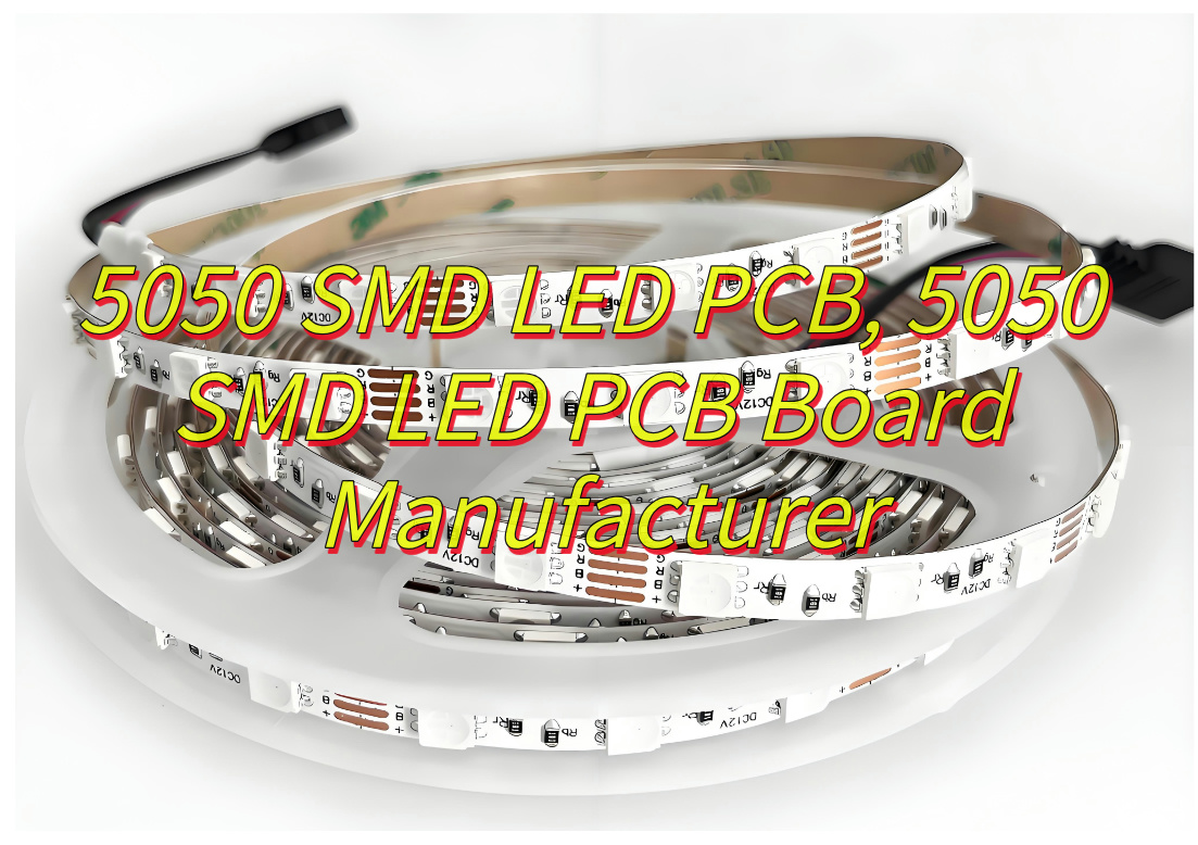
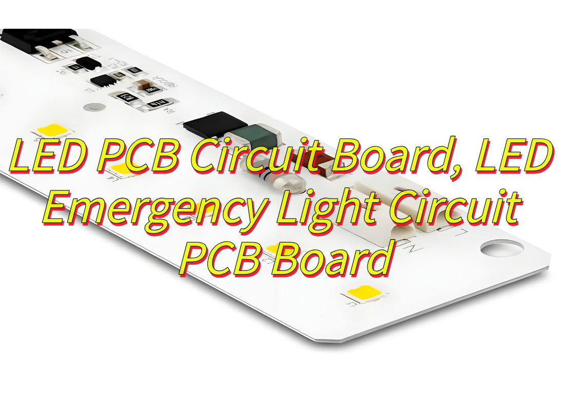
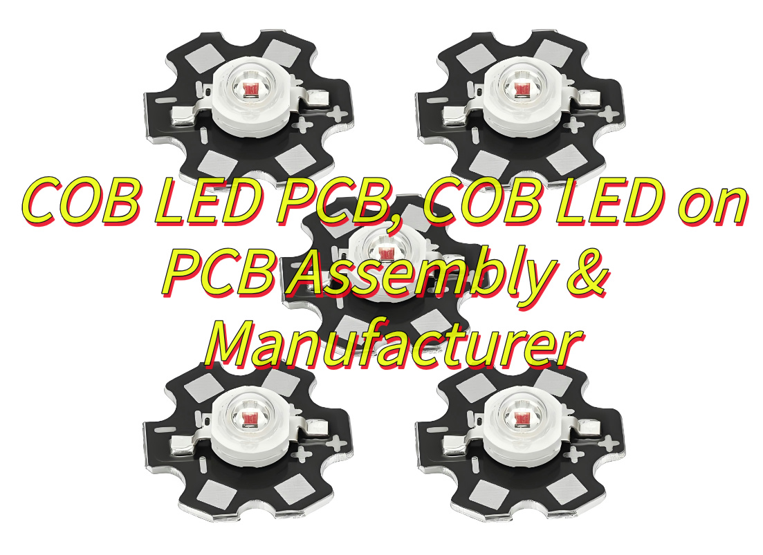
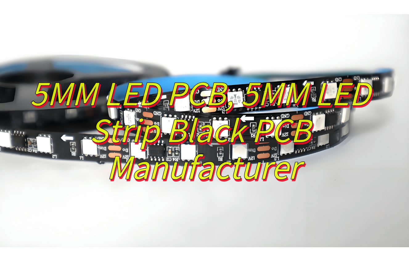
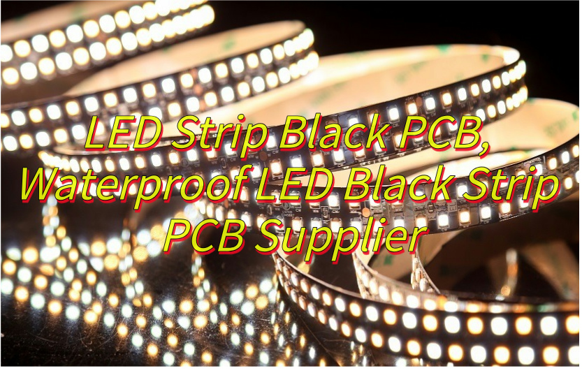
What Is LED Strip Black PCB?
A LED strip black PCB is a specialized printed circuit board designed specifically for LED strip lighting applications, characterized by its dark-colored substrate that serves both functional and aesthetic purposes. The black coloration typically comes from a dark solder mask or specialized substrate materials like black FR4 for rigid boards or black polyimide for flexible versions. This design enhances visual contrast with mounted LEDs while reducing light reflection between components, particularly beneficial for RGB lighting systems where color accuracy matters. The dark surface helps absorb stray light, preventing color distortion and improving overall light output quality in applications ranging from architectural lighting to automotive accents. Beyond optical benefits, the black PCB construction maintains standard electrical properties while offering improved heat dissipation for high-power LED arrays. Manufacturers produce these boards with precision trace layouts to ensure even current distribution along the entire strip length, supporting various LED configurations including 2835, 5050, and COB packages. The production process requires careful control of solder mask application to achieve consistent darkness without compromising insulation or conductivity. When combined with white silkscreen markings, the black PCB creates an optimized platform that balances technical performance with sleek visual appeal in modern lighting designs.
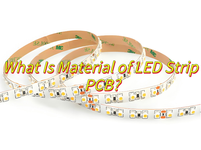
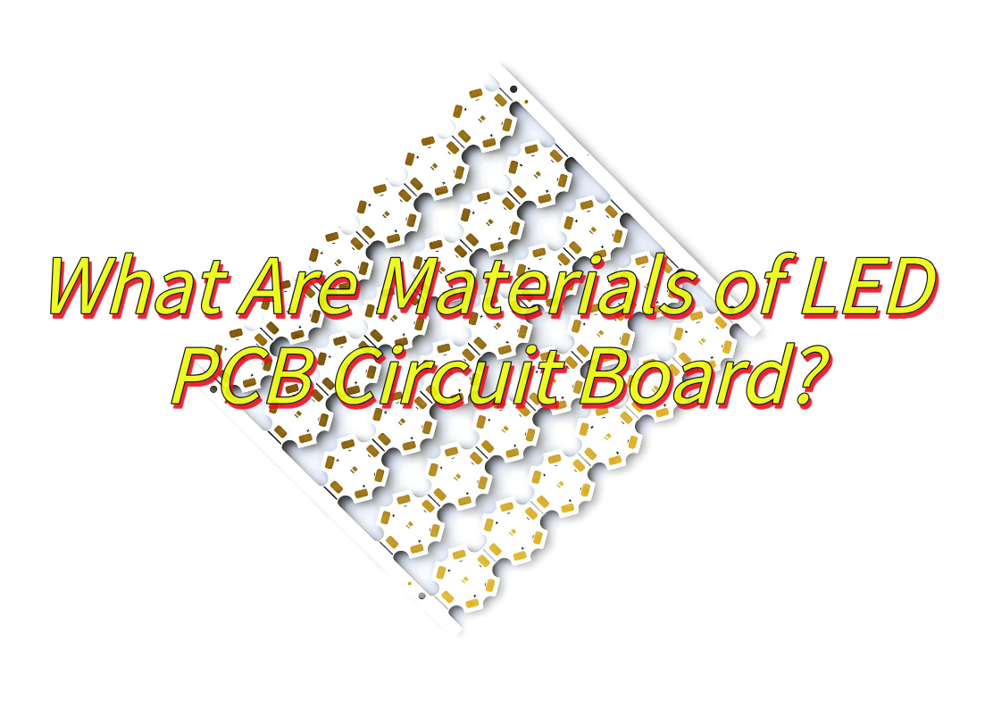
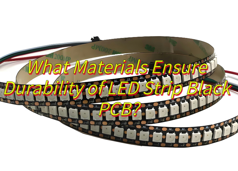
What Materials Ensure Durability of LED Strip Black PCB?
Here are materials ensure durability of LED strip black PCB:
Substrate Materials:
- FR-4 glass fiber epoxy laminates provide mechanical rigidity and thermal stability, essential for LED strips in indoor fixtures.
- Flexible polyimide (PI) substrates enable bending in curved installations like automotive interiors or signage.
Conductive Layers:
- Electroplated copper (1oz–2oz thickness) ensures efficient current distribution for high-density LED arrays.
- Rolled annealed copper foil reduces cracking risks during repeated flexing in wearable or kinetic lighting designs.
Solder Mask:
- High-temperature resistant black epoxy ink minimizes light bleed between LEDs while protecting traces from oxidation.
- UV-blocking additives prevent yellowing under prolonged LED exposure, maintaining aesthetic consistency.
Thermal Interface Materials:
- Thermal conductive pads or silicone-based greases improve heat dissipation from LED junctions to the substrate.
- Metal-core PCB variants (MCPCB) with aluminum layers enhance thermal management for high-power applications.
Protective Coatings:
- Conformal coatings (acrylic, polyurethane) shield against moisture, dust, and chemicals in industrial environments.
- Parylene deposition offers ultra-thin, pinhole-free protection for LED strips in medical or marine settings.
Adhesive Systems:
- Pressure-sensitive adhesives (PSA) with 3M 9448 or equivalent ratings ensure secure mounting on various surfaces.
- High-bond tapes resist cold flow under prolonged thermal cycling in outdoor LED installations.
Component Packaging:
- LEDs with silicone encapsulation resist UV degradation and temperature fluctuations.
- SMD resistors and capacitors rated for 120°C operation prevent premature failure in high-heat environments.
Connector Materials:
- Gold-plated pins on JST or Molex connectors prevent corrosion in humid conditions.
- Silicone-jacketed wires maintain flexibility at -40°C to +80°C for extreme climate applications.
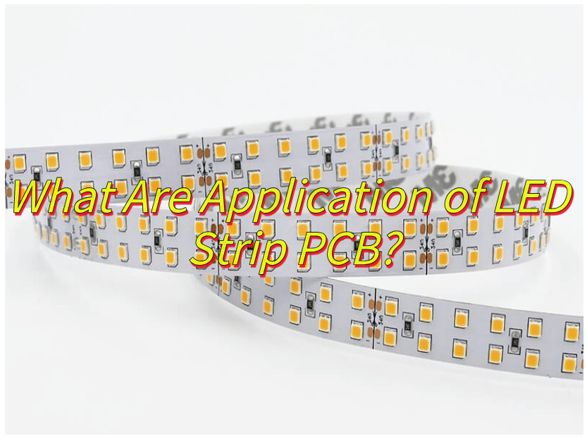
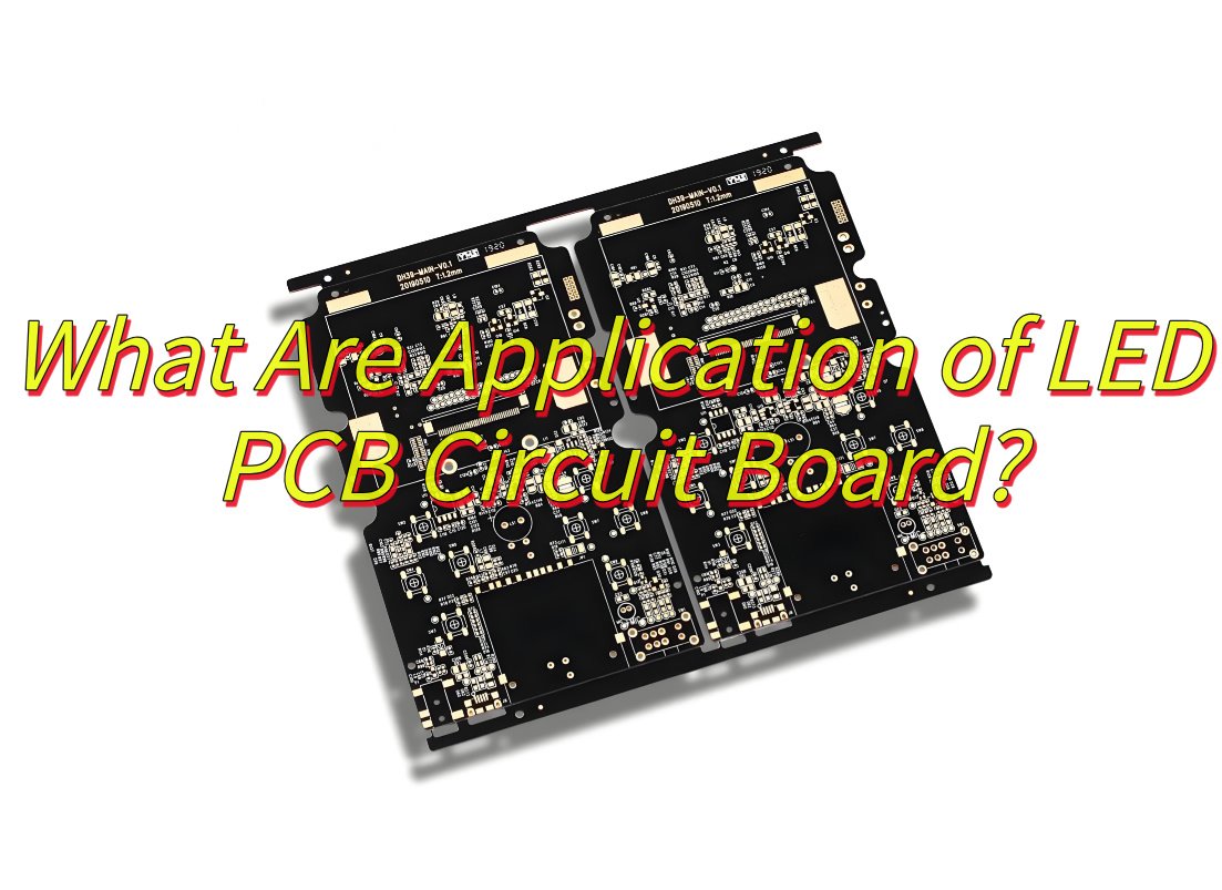
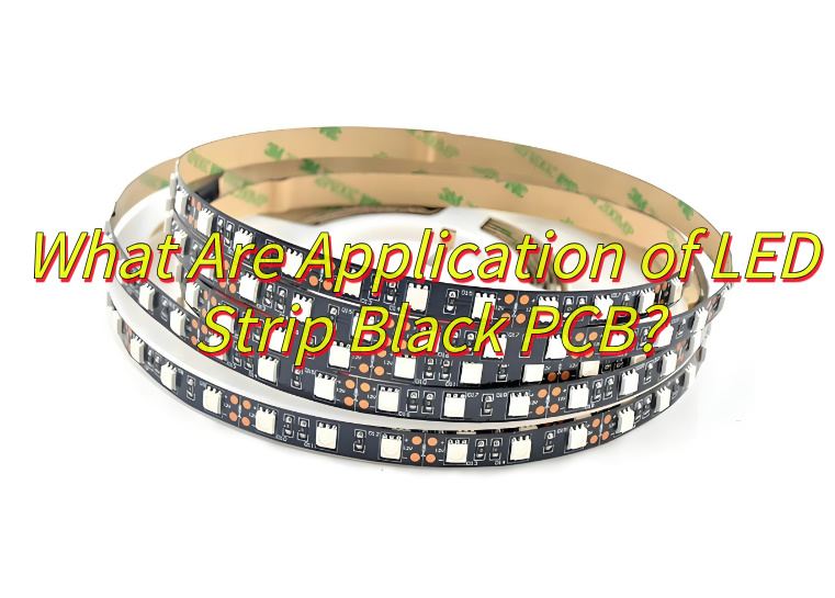
What Are Application of LED Strip Black PCB?
Application of LED strip black PCB:
- Architectural Lighting Systems: LED strip black PCBs enable discreet installation in coves and recesses where the dark substrate blends with shadows. The non-reflective surface prevents light pollution in high-end interior designs.
- Automotive Underglow Lighting: Vehicle manufacturers utilize black PCB strips for their heat resistance and sleek appearance. The dark background enhances color saturation in dynamic RGB lighting systems.
- Retail Display Enhancement: Black PCBs create focused illumination without visible circuit traces, making them ideal for luxury product showcases. The contrast makes LED colors appear more vibrant.
- Home Theater Lighting: Theater installers prefer black PCBs for their light-absorbing qualities that prevent screen glare. They maintain darkness when not in use while providing ambient lighting.
- Commercial Signage: Backlit letters and channel letters benefit from black PCB strips that disappear when viewed from certain angles. This creates floating light effects for business signage.
- Stage and Event Lighting: Production companies deploy flexible black PCB strips for truss lighting and set designs. The dark base minimizes unwanted light spill during performances.
- Marine and Pool Lighting: Waterproof black PCB strips withstand humid environments while providing underwater illumination. The dark color resists algae growth in pool applications.
- Museum Art Lighting: Curators select black PCB strips for their ability to highlight artworks without visible light sources. The precise beam control prevents damage to sensitive pigments.
- Industrial Machine Lighting: Factory equipment incorporates rugged black PCB strips for task lighting. The durable construction resists vibration and chemical exposure.
- Smart Home Integration: Black PCB strips pair with control systems for automated lighting scenarios. Their discreet appearance blends with modern interiors.
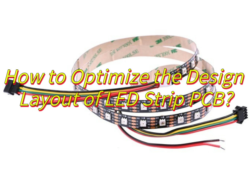
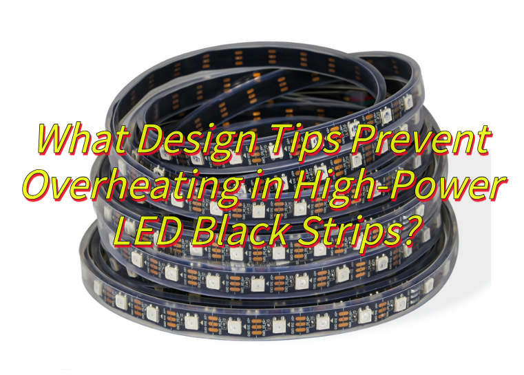
What Design Tips Prevent Overheating in High-Power LED Black Strips?
Here are design tips about how to prevent overheating in high-power LED black strips:
- Thermal Conductivity Optimization: Use aluminum-backed MCPCB (Metal Core PCB) substrates to enhance heat dissipation from LED junctions. The metal core acts as a heat sink, reducing thermal resistance compared to standard FR-4 boards.
- Copper Trace Width Enhancement: Increase copper foil thickness (e.g., 2oz vs. 1oz) and trace widths to lower electrical resistance. Wider traces minimize voltage drop and heat generation across high-power LED arrays.
- Thermal Vias Placement: Strategically position plated thermal vias beneath LED pads to transfer heat to the PCB’s opposite side. This improves vertical heat conduction to attached heat sinks or housing.
- Component Spacing: Maintain ≥5mm gaps between adjacent high-power LEDs to prevent heat pooling. Adequate spacing allows convective airflow and reduces localized temperature spikes.
- LED Driver Integration: Embed DC-DC converters directly on the PCB to minimize wiring losses. Onboard drivers reduce resistance-induced heat from external connections.
- Surface Finish Selection: Choose ENIG (Electroless Nickel Immersion Gold) over HASL to improve solder joint reliability under thermal cycling. ENIG’s flat surface also enhances heat transfer to components.
- Ambient Temperature Derating: Design circuits to operate at ≤80% of maximum rated current when ambient temperatures exceed 25°C. This compensates for reduced heat sink efficiency in hot environments.
- Thermal Simulation Testing: Validate designs using IR thermal cameras to identify hotspots pre-production. Adjust PCB layout or material thickness based on simulated worst-case scenarios.
How to Choose A Waterproof LED Black Strip PCB Supplier?
Here’s how to choose a waterproof LED black strip PCB supplier:
- Material Quality Assurance: Prioritize suppliers using high-grade substrates like FR-4 or flexible polyimide for 45cm LED strip waterproof black PCB variants. Ensure their black solder mask includes UV-resistant epoxy to prevent yellowing in outdoor RGB LED strip black PCB applications.
- Customization Flexibility: Confirm they offer length options (e.g., 1m Microcenter or 3ft strips) and LED density variants (e.g., 60cm yellow 600 LED flexible strips). Verify if they accommodate IP65-rated enclosures with silicone glue or potting compounds for moisture protection.
- Thermal Management Expertise: Evaluate if they optimize copper trace widths and thermal via placement for high-power RGB configurations. Ask about MCPCB (Metal Core PCB) options to improve heat dissipation in dense LED arrays.
- Waterproofing Processes: Inspect their conformal coating application methods for black PCB strip LEDs IP65. Ensure they use 360-degree silicone sealing on connectors and test under prolonged submersion or high-humidity conditions.
- Color Consistency Controls: Check if they employ automated optical inspection (AOI) to maintain uniform RGB color rendering across batches. Request binning reports for LEDs to ensure ≤3% brightness variation in white light outputs.
- Flexural Durability Testing: For ultra-thin designs, verify they conduct bend cycle tests (e.g., 10,000+ folds at 10mm radius) on polyimide-based strips. Confirm compatibility with aluminum channels to prevent delamination in curved installations.
- Certification Compliance: Ensure products meet UL 94V-0 flammability ratings and RoHS directives. For automotive or marine use, confirm AEC-Q102 qualification for LED components in 60cm yellow flexible strips.
- Lead Time & Scalability: Assess if they offer rapid prototyping (e.g., 24-hour turnaround for 1m samples) while maintaining lot-to-lot consistency. Check if their SMT lines handle mixed-technology boards (through-hole connectors + SMD LEDs) for hybrid designs.
How Do We Ensure Durability in Waterproof LED Black Strip PCB Production?
Here are methods about how do we ensure durability in waterproof LED black strip PCB production:
- Substrate Material Selection: Use high-TG FR-4 or polyimide substrates with moisture absorption <0.2% to prevent warping in humid environments. For flexible variants, specify 2-layer copper-clad polyimide with 35µm copper thickness for enhanced durability during bending.
- LED Chip Quality Control: Source SMD LED chips with LM-80 certification to ensure lumen maintenance >90% after 6,000 hours. Implement binning processes to maintain Δuv <0.005 color consistency across batches.
- Encapsulation Technology: Apply medical-grade silicone (Shore A hardness 30–40) via vacuum dispensing to eliminate bubbles. Cure at 150°C for 2 hours to achieve 1.5mm encapsulation thickness with >90% light transmittance.
- Solder Joint Reliability: Employ lead-free HASL finish with nickel barrier layer to resist corrosion. Perform 3D X-ray inspection to detect voids >5% in solder joints, ensuring compliance with IPC-A-610 Class 3 standards.
- Connector Sealing Method: Use overmolded M12 waterproof connectors with PBT housing and silicone O-rings. Validate IP67 compliance via 1 meter/30-minute submersion tests with 0.2MPa pressure.
- Flexural Endurance Testing: For ultra-thin 0.4mm boards, conduct dynamic bend tests at 5mm radius, 180° folds for 10,000 cycles. Measure resistance change <2% using micro-ohmmeter post-testing.
- Thermal Shock Resistance: Subject assemblies to -40°C/+125°C thermal cycling for 500 cycles. Verify functionality using integrated circuit testing, ensuring no failures in LED drivers or control chips.
- UV Exposure Mitigation: Apply UV-blocking conformal coating with 3% titanium dioxide content. Test via QUV accelerated weathering (ASTM G154) for 1,000 hours, measuring ΔE <2.5 color shift.
- Chemical Resistance Protocol: Test PCBs against 5% NaCl solution, automotive fluids, and cleaning agents. Ensure no delamination or corrosion using SEM analysis after 96-hour immersion.
- Electrical Safety Verification: Perform 1,500VAC Hipot testing for 1 second on final assemblies. Measure insulation resistance >100MΩ at 500VDC, ensuring compliance with IEC 60598-2-20 standards.
How to Test the Quality of Waterproof LED Black Strip PCB?
This is how to test the quality of waterproof LED black strip PCB:
Visual Inspection & Structural Integrity Verification
- Surface Analysis: Use a high-magnification microscope to inspect the black solder mask for uniformity, pinholes, or delamination. LED placement accuracy must be within ±0.1mm to ensure consistent light output.
- Encapsulation Review: Validate silicone coating thickness (≥1.5mm) and light transmittance (>90%) using a spectrophotometer. Check for bubbles or impurities that could compromise waterproofing.
Environmental Durability Testing
- Immersion & Pressure Resistance: Submerge the PCB in 1-meter-deep water for 72 hours (IP67 compliance). Monitor for internal condensation or insulation resistance drops (>100MΩ required).
- Thermal Cycling: Expose to -40°C to +85°C for 100 cycles at 85% RH. Measure LED color shift (Δu’v’ <0.005) and solder joint integrity via infrared thermography.
- UV Exposure: Test under QUV chambers for 1,000 hours (ASTM G154). Ensure yellowing index (ΔE) <3 and maintain optical performance.
Mechanical Endurance Trials
- Flexural Testing: Bend flexible strips 10,000+ times at a 5mm radius. Detect copper trace cracks using laser Doppler vibrometry and verify light output decay (<5%).
- Vibration Resistance: Subject to 20G RMS vibrations (10–2,000Hz) for 8 hours. Confirm no LED dislodgment or electrical failures using optical power meters.
Electrical Performance & Safety Assessment
- High-Potential Testing: Apply 1,500VAC for 60 seconds. Ensure no arcing or breakdown using partial discharge detectors; maintain insulation resistance >100MΩ.
- Thermal Shock: Cycle between -25°C and +125°C for 300 cycles. Validate LED lifespan (L70 >50,000 hours) and driver chip stability.
- Current Overload: Operate at 120% rated current for 24 hours. Log junction temperatures (Tj <120°C) and monitor luminous flux decay (<10%).
Connector & Interface Reliability
- Mating Cycle Test: Perform 1,000 insertions/withdrawals on waterproof connectors. Check contact resistance (<30mΩ) and seal integrity (compression set <10%).
- Salt Spray Corrosion: Expose to 5% NaCl solution for 96 hours. Assess metal components for corrosion (rating ≥9/10) and electrical continuity.
Optical Consistency Evaluation
- Spectral Analysis: Measure CIE 1931 coordinates across 25 points on 1-meter strips. Ensure batch-to-batch consistency (Δu’v’ <0.002) and CRI >80 for white LEDs.
- Luminance Uniformity: Test illuminance at 25 points; require >90% uniformity to eliminate dark spots or glare.
Long-Term Reliability Monitoring
- Accelerated Aging: Operate at 85°C/85% RH for 5,000 hours. Track luminous flux decay (<15%) and color temperature drift (<300K).
- Failure Analysis: Conduct SEM/EDS on failed samples to identify root causes (e.g., voids, cracks) and refine manufacturing processes.
Can LED Strip Black PCB Be Customized for Specialized Applications?
Yes, LED strip black PCB can be customized for specialized applications through a range of technical adaptations tailored to meet unique operational demands:
Material Flexibility:
- Substrates like high-TG FR-4, aluminum based MCPCB, or polyimide are selected based on thermal conductivity, flexibility, or moisture resistance requirements. Waterproof variants incorporate hydrophobic coatings or silicone encapsulation to achieve IP65–IP68 ratings.
Circuit Optimization:
- Trace widths, copper thickness, and thermal via placement are adjusted to manage current loads (e.g., 6A/meter for high-power strips). Metal-core layers improve heat dissipation in dense LED arrays.
LED Configuration:
- Customizable parameters include LED density (30–600 LEDs/meter), color temperatures (2700K–6500K), and spectral outputs (e.g., UV for curing or RGB for decorative lighting).
Connector & Interface Design:
- Waterproof connectors with silicone gaskets ensure IP67 compliance. Custom wire lengths, pinouts, and strain reliefs accommodate installation constraints.
Thermal Management Solutions:
- Integrated heat sinks, graphite layers, or aluminum housing reduce junction temperatures. For LED strip black PCB, thermal pads beneath LEDs enhance heat conduction through silicone barriers.
Control Integration:
- Onboard drivers support dimming protocols (0–10V, DALI, PWM) or wireless communication (Bluetooth, Zigbee) for smart automation in commercial or residential settings.
Optical Enhancements:
- Secondary optics (e.g., 120° lenses) or diffusers ensure uniform illumination. Anti-glare coatings minimize light trespass in architectural or automotive applications.
Environmental Resistance:
- Conformal coatings (parylene, acrylic) and triple-sealed edges protect against chemicals, UV, and extreme temperatures (-40°C to +125°C).
Certification Compliance:
- Designs adhere to UL, RoHS, or IEC standards. Automotive-grade variants meet AEC-Q102 requirements for vibration and thermal cycling resistance.
Form Factor Adaptations:
- Rigid-flex PCBs combine rigid sections (for connectors) with flexible zones (for curved installations). Ultra-thin (0.4mm) designs fit into narrow gaps in consumer electronics.
Conclusion
LED strip black PCB platforms are engineered for reliability, combining robust materials like FR-4 or aluminum-backed MCPCB with advanced thermal designs to resist heat and harsh environments. Their adaptability spans automotive, architectural, and industrial lighting, supported by customizable LED configurations and smart controls. Selecting a supplier requires evaluating certifications, material quality, and rigorous testing—such as submersion, thermal cycling, and UV exposure—to ensure performance. Manufacturers enhance durability through hydrophobic coatings, precise solder joint protocols, and optical consistency checks. For specialized needs, these PCBs integrate features like rigid-flex form factors or UV-resistant coatings, making them indispensable for demanding applications. By prioritizing technical expertise and quality assurance, suppliers deliver LED strip black PCB solutions that exceed expectations in functionality and longevity.