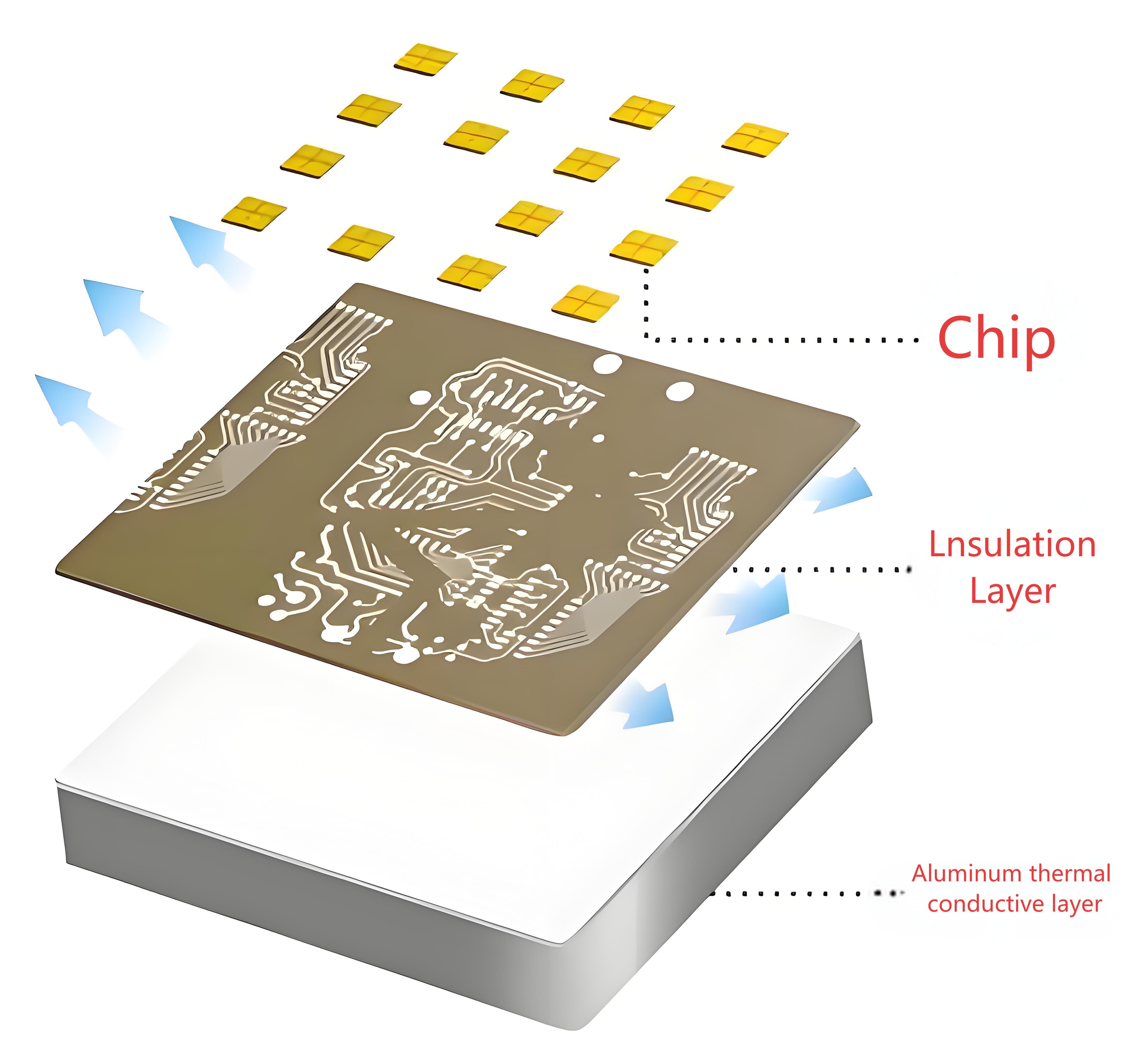
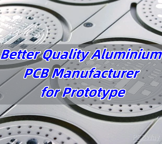
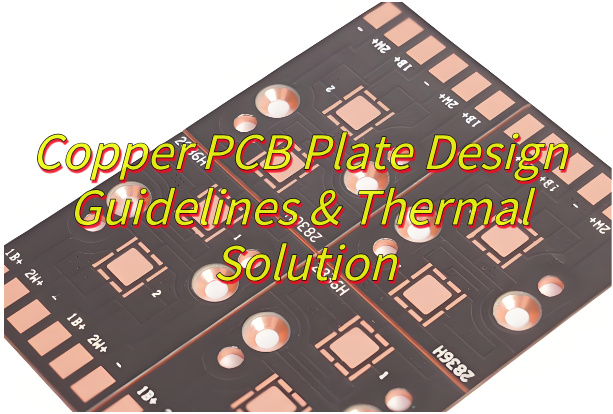
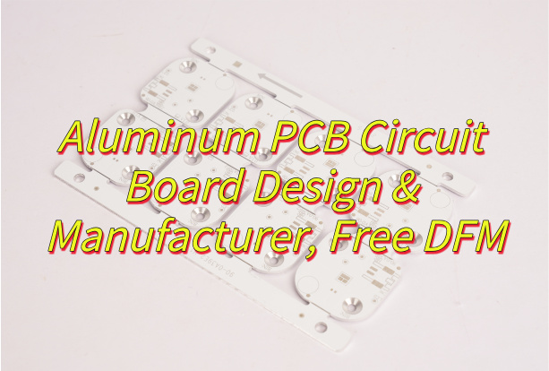
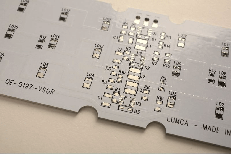
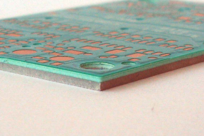
IMS PCB definition refers to a printed circuit board built on an Insulated Metal Substrate, primarily designed for excellent heat dissipation. This structure supports high-power components and keeps temperatures under control. While many boards rely on FR4, IMS stands out where thermal stress is high.
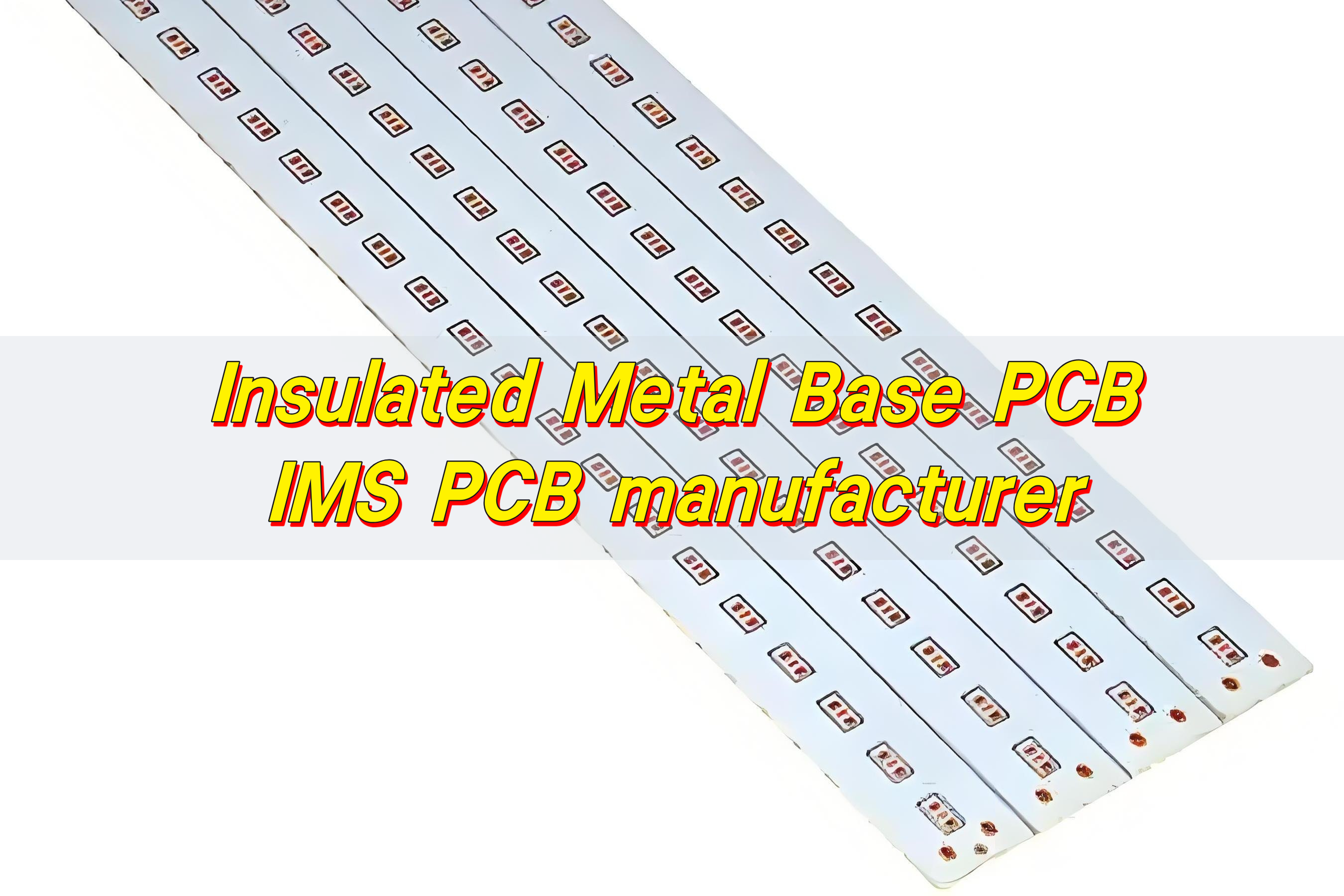
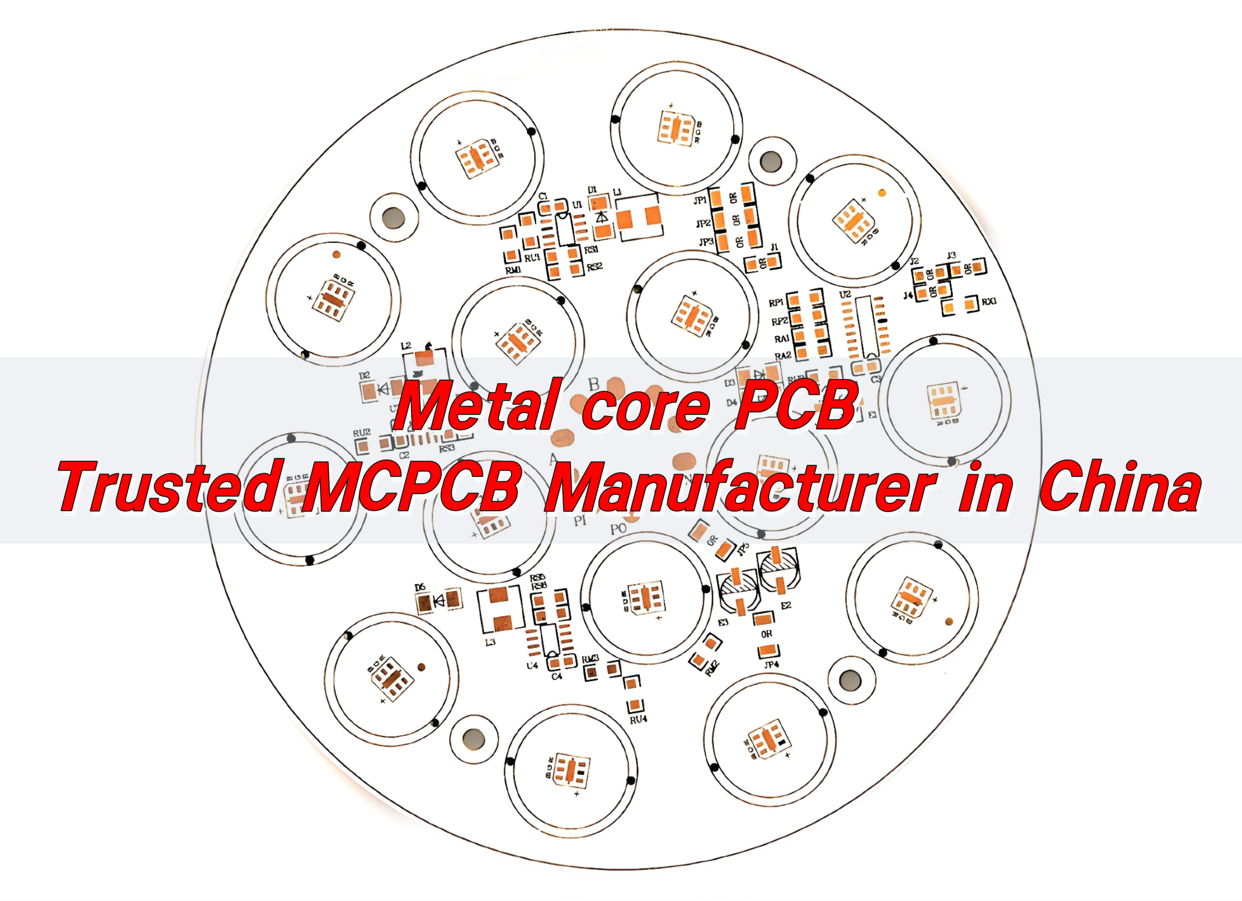
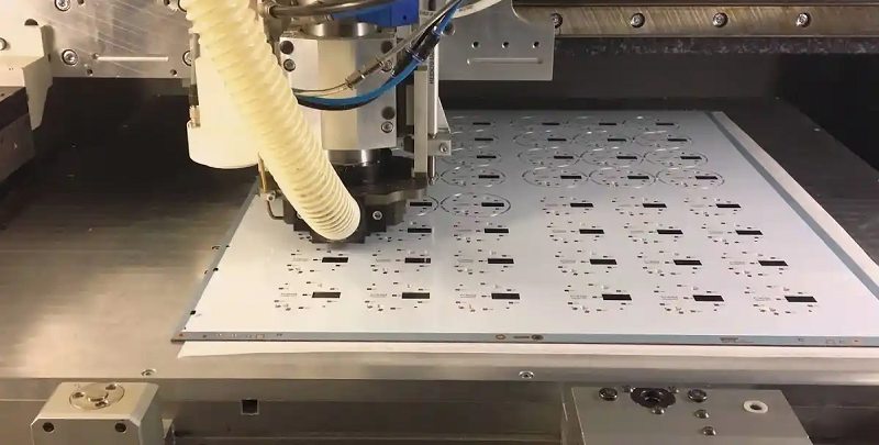
EBest Circuit (Best Technology) is a top-tier IMS PCB manufacturer and PCBA service provider in China. Since 2006, we have gained great first-hand experience in dealing with thermal management challenges in customers’ compact designs and providing full solutions to customers for their inadequate heat dissipation in high-power applications. Our factory has passed certifications like ISO 9001, ISO 13485, IATF 16949, AS9100D. Our factory has the full qualification to manufacture reliable IMS PCBs and PCBA to the market.
IMS PCBs stand out through their metal-core structure, thermal dielectric layer, and suitability for high-power applications—delivering up to 80% better heat dissipation than FR4. If you have any doubts about the IMS PCB definition or you require more advice from us, please make a call to +86-755-2909-1601 or send your Gerber file and special requirement details to us at sales@bestpcbs.com.
What is IMS PCB Definition?
To understand the IMS PCB Definition, we need to break it down into three main aspects:
- Metal-core construction: IMS PCBs use a metal base such as aluminum or copper. This helps draw heat away from components faster than FR4 materials.
- Thermal dielectric layer: Between the copper circuitry and the metal base lies a special dielectric layer, usually 0.05–0.20mm thick. This layer balances electrical insulation and thermal conductivity.
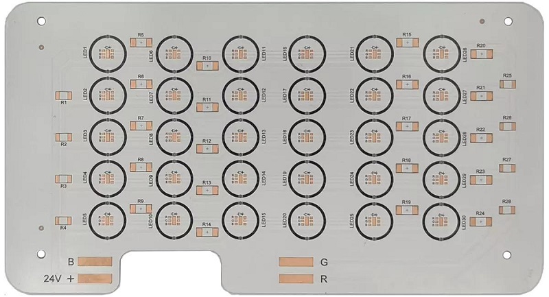
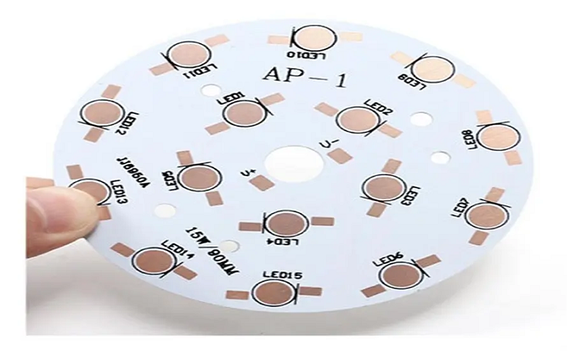
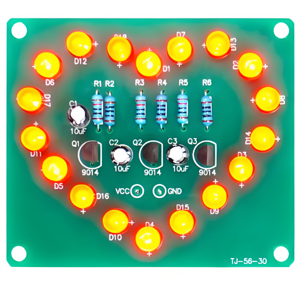
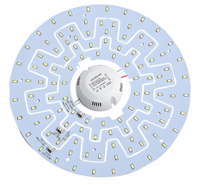
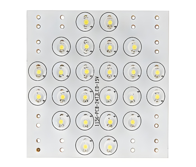
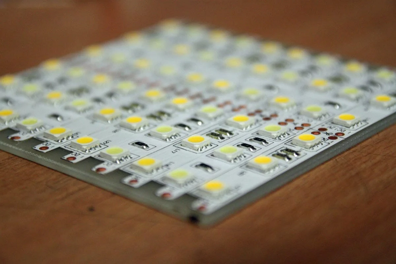
- High-power applications: IMS PCBs are built for products that produce significant heat like LEDs, power modules, and automotive electronics. Their construction makes them dependable even under high thermal load.
When these three focus areas are optimized, the thermal performance of IMS PCB can reach up to 80% better than FR4 PCBs. This is due to the metal base’s superior conductivity and the efficient stack-up structure. In short, IMS PCB is engineered for reliability in thermally demanding environments.
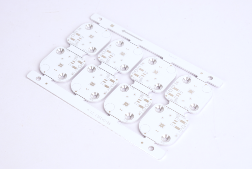
What Are the Types of IMS PCB?
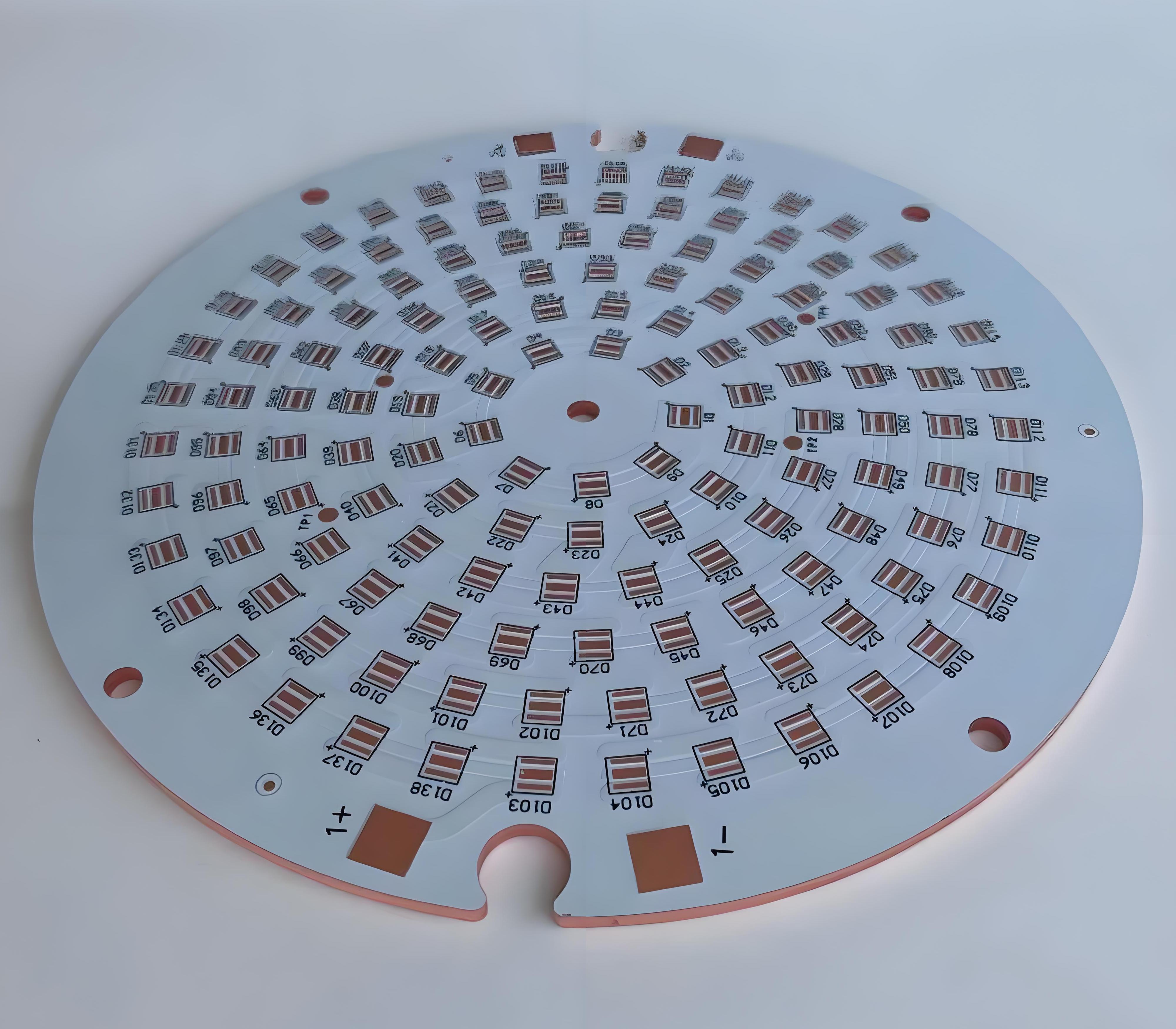
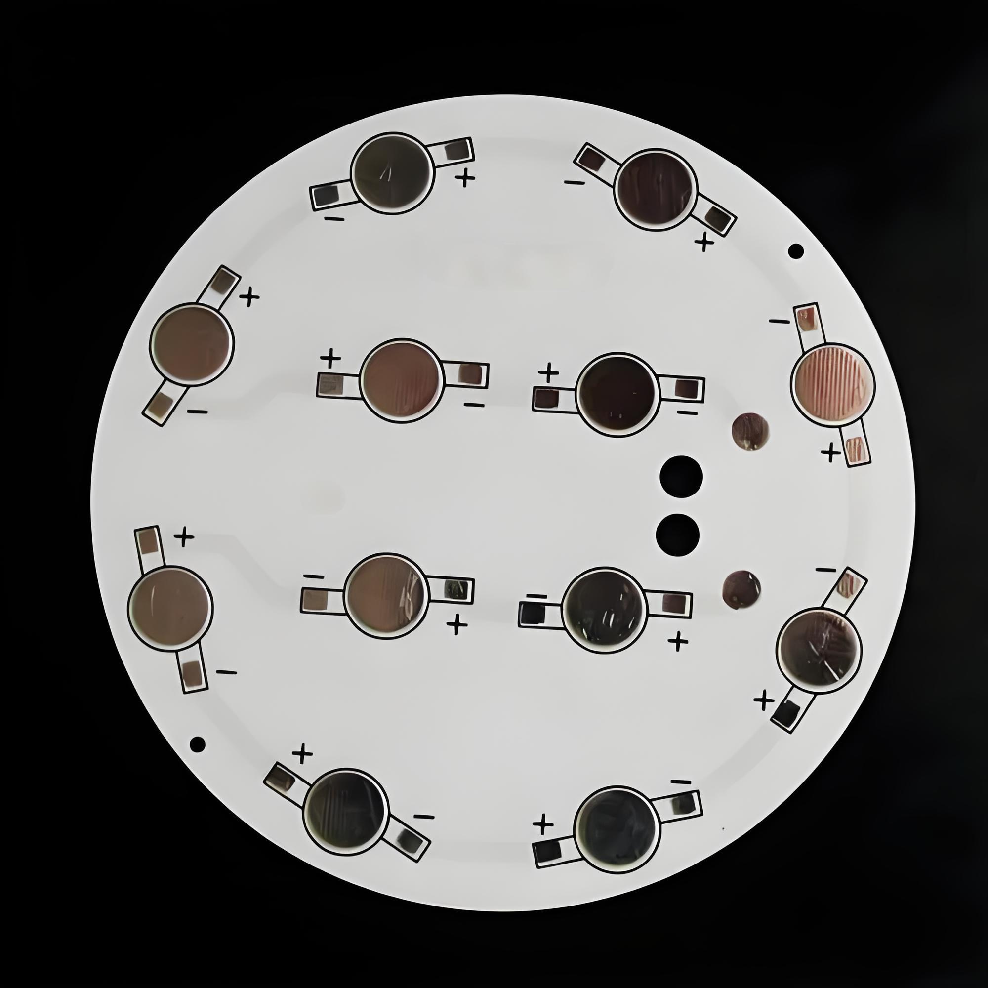
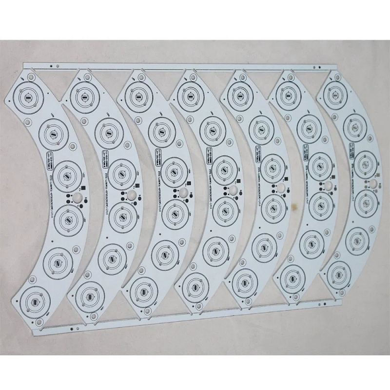
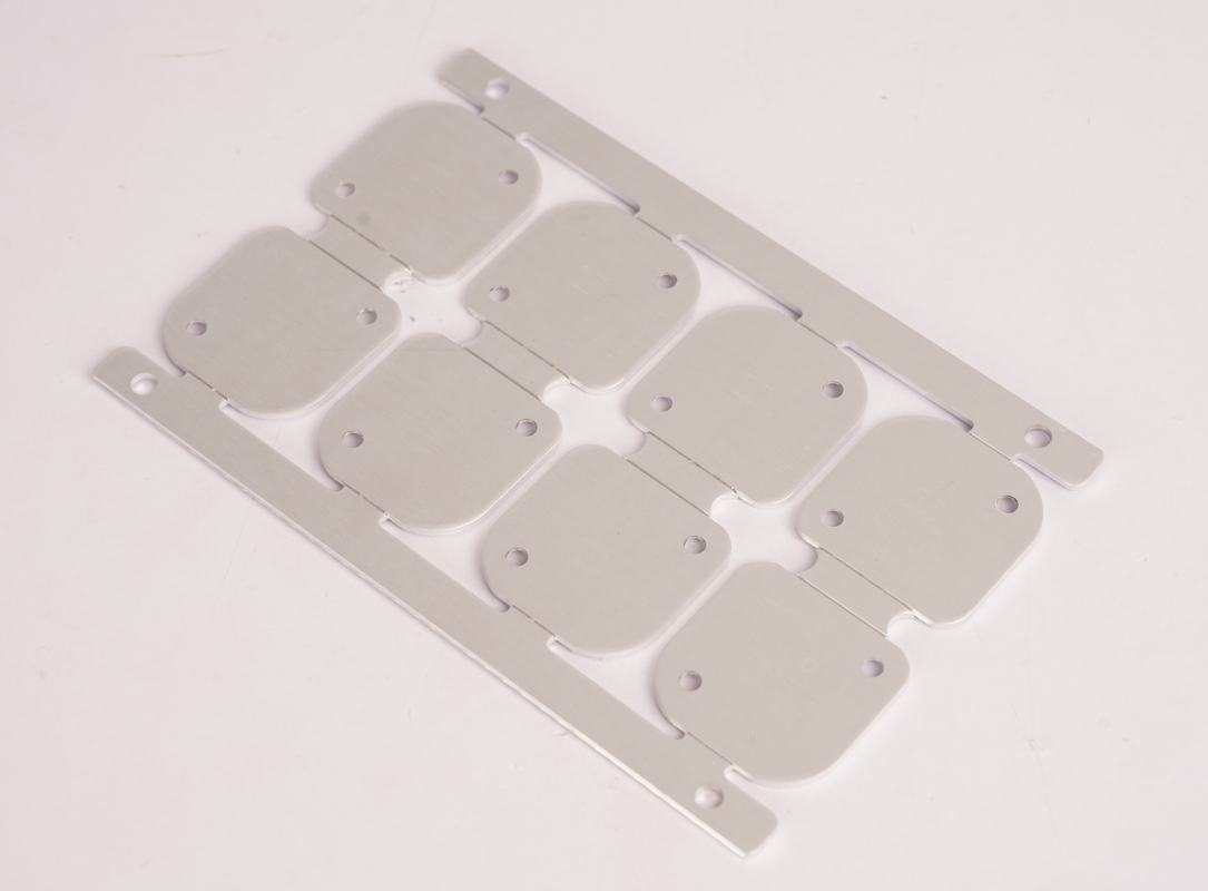
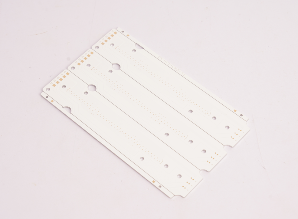
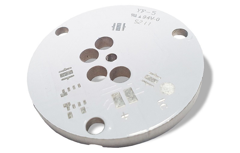
There are mainly two types based on the base metal: Aluminum-based IMS PCB and Copper-based IMS PCB. IMS PCBs (Insulated Metal Substrate PCBs) come in several types depending on their structure and application needs. Each type offers unique benefits to match specific electrical, thermal, and mechanical demands. Here are the most common ones:
1. Flexible Aluminum IMS PCB
This type uses a flexible dielectric layer combined with aluminum alloys such as 5754. It can bend and conform to curved surfaces without cracking, making it ideal for wearable devices, foldable modules, or curved LED lighting. The flexibility doesn’t sacrifice thermal performance, which makes it suitable for tight and dynamic installation spaces.
2. Hybrid Aluminum IMS PCB
Hybrid types combine traditional FR4 multilayer cores (like 2-layer or 4-layer boards) with an aluminum base using thermally conductive adhesives. This structure lowers cost while still improving heat dissipation over standard FR4. It’s commonly used in RF applications or areas that need better EMI shielding along with moderate thermal control.
3. Multilayer Aluminum IMS PCB
Designed for high complexity systems, this type stacks multiple dielectric layers and may include blind vias or thermal vias. It supports dense circuit routing, power management, and thermal paths within the same board. Applications include industrial power supplies and advanced motor controls where both thermal and signal integrity are critical.
4. Through-Hole Aluminum IMS PCB
Here, the aluminum base acts as a mechanical and thermal “core” for multilayer construction. Plated through holes enable either full electrical connection or insulation, depending on design. This type is well-suited for high-current modules, including automotive charging systems or power converters, where mechanical strength and efficient heat transfer are equally important.
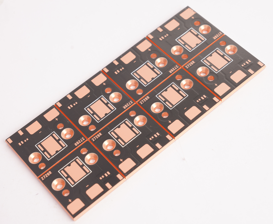
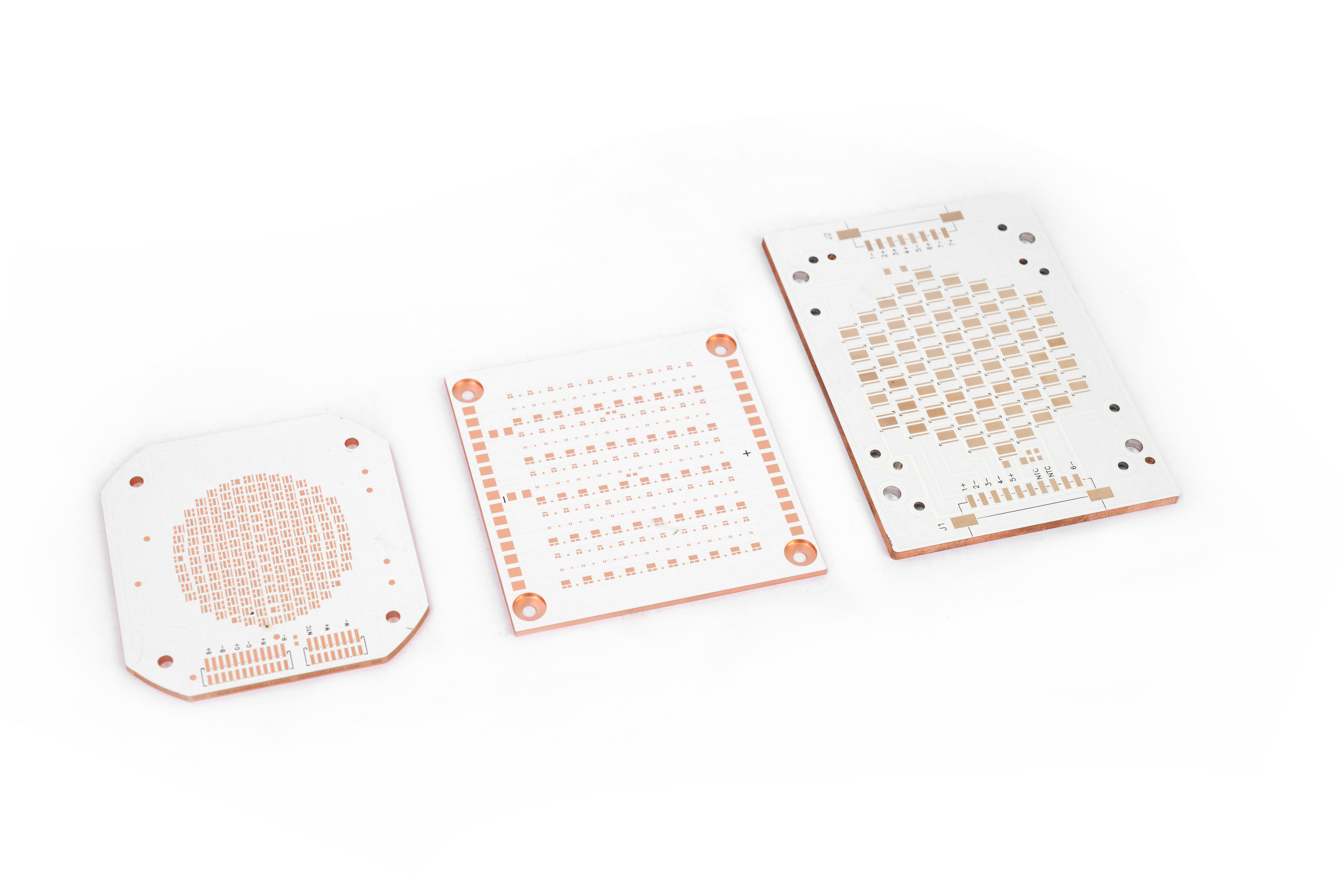
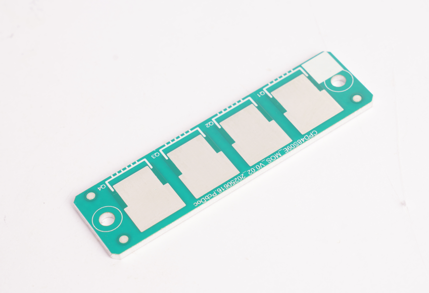
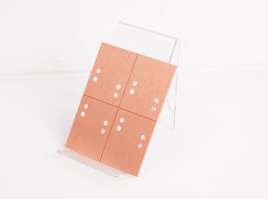
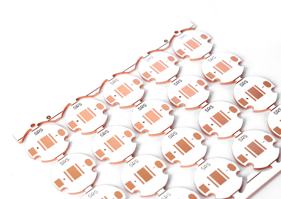
5. Copper-Based IMS PCB
Instead of aluminum, this version uses copper (like C1100) as the metal core, offering much higher thermal conductivity—around 400 W/m·K. Though more expensive, copper IMS PCBs are unmatched in heat management and are often used in extreme environments, such as high-frequency power electronics, laser systems, or high-intensity LED drivers.
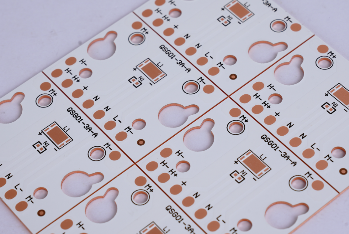
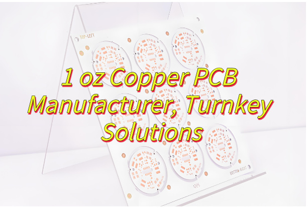
What Are the Common Thicknesses of Copper Substrate IMS PCB?
Copper thickness matters in heat spreading and current capacity. Common thicknesses are:
- 1 oz (35μm) – standard, used in most designs
- 2 oz (70μm) – better for power and thermal needs
- 3 oz to 6 oz – for heavy-duty applications
Choosing the right copper thickness balances cost, weight, and performance. It depends on the device’s power level and thermal load.
What is a FR4 PCB in Electrical Terms?
FR4 PCB uses a glass-reinforced epoxy laminate as the core. It is widely used due to its low cost and electrical stability. But it is not built for heat-heavy conditions. FR4 struggles when components generate high thermal energy. Let’s take a closer look at its detailed features.
1. Material and Structure
FR4 stands for “Flame Retardant level 4,” a UL94 V-0 rated material that self-extinguishes when ignited, enhancing electrical safety. The board is constructed by laminating layers of glass fiber for mechanical strength and epoxy resin for electrical insulation. This results in a durable, uniform substrate that supports multi-layer circuit builds.
2. Electrical Properties
One of the main reasons FR4 remains a popular choice is its reliable electrical insulation. It provides an insulation resistance between 10¹² to 10¹⁵Ω, effectively separating circuit paths.
Key dielectric characteristics include:
- Dielectric constant (Dk) between 4.0 to 4.7 – this affects how fast signals move through the PCB.
- Dissipation factor (Df) between 0.01 to 0.03 – indicating low signal loss, suitable for medium to high-frequency applications.
These properties help maintain signal clarity, especially in digital and RF circuits.
3. Thermal and Mechanical Performance
FR4 PCBs generally operate within a temperature range of 130°C to 180°C, which covers most consumer and industrial electronics.
They also exhibit excellent mechanical stability, showing minimal warping under humidity or temperature fluctuations. This consistency makes FR4 a solid choice for high-precision multilayer PCB manufacturing.
4. Manufacturing and Application Benefits
- Cost-Effective: FR4 is one of the most affordable and widely available materials. Its mature production process supports mass production with consistent results.
- Good Workability: It can be easily cut, drilled, and etched to fit complex layouts, which speeds up prototyping and full-scale fabrication.
- Versatile Applications: It’s used in everything from mobile phones and computers to control boards, sensors, and consumer electronics.
However, when the circuit involves high power or heat—such as in LED drivers, automotive modules, or power converters—FR4 may fall short in thermal performance. In those cases, materials like IMS offer better thermal conductivity and system reliability. IMS PCB transfers heat 80% faster than FR4 in many setups.
| Material | Thermal Conductivity (W/mK) | vs. FR4 |
| FR4 | 0.1–0.5 | Baseline |
| IMS Dielectric | 1.0–12.0 | 8–12× higher |
| Aluminum Core | ~200 | 400–1000× higher |
| Copper Core | ~400 | 800–1600× higher |
Why is IMS Needed?
Electronics are smaller, faster, and more powerful. This generates more heat in tighter spaces. FR4 boards can’t always manage that heat. When parts overheat, performance drops or fails entirely. IMS provides a way out. It pulls heat away from hot spots and extends product life. It keeps temperatures low and improves reliability.
Also, IMS helps reduce the size of heatsinks or external cooling. This saves space and weight, especially in automotive and lighting systems.
What Factors Affect the Quality of Thermal Separation IMS PCB?
Several key elements decide how well IMS handles heat:
- Dielectric Layer Quality: The thinner and more thermally conductive the layer, the better the heat transfer.
- Copper Thickness: More copper helps move heat faster.
- Metal Base Type: Copper performs better but costs more.
- Bonding Strength: A strong bond between layers ensures stable performance and durability.
At EBest Circuit (Best Technology), we keep strict control over each of these steps. We use advanced testing tools like TDR and thermal shock tests to validate heat performance and bonding quality.
Why Choose EBest Circuit (Best Technology) as Your Major IMS PCB Manufacturer?
Customers face real concerns when sourcing IMS PCBs. Some suppliers deliver inconsistent quality. Others delay shipments or use low-grade raw materials. These issues cost time and damage trust.
EBest Circuit (Best Technology) solves these headaches:
- Traceability: Every board’s raw material can be traced through our MES system. This avoids counterfeit risks.
- Certifications: We hold ISO 9001, ISO 13485 for medical, IATF 16949 for automotive, and AS9100D for aerospace. This proves our strict quality control.
- Stable Lead Time: We stick to schedules, even in tight demand cycles. Our in-house capacity and vendor network help achieve this.
- Engineering Support: From DFM checks to prototype validation, our team gives solid advice and practical solutions.
- Full Solutions: We support a rich product line, such as IMS PCB, MCPCB, rigid, flex, rigid-flex, ceramic PCBs, and PCBA. Whatever substrate you need, such as FR-4, high Tg FR-4, halogen-free FR-4, metal core, copper core, ceramic, Low Dk/Df (ISOLA/ Rogers), our engineers have extensive experience to suggest viable PCBs for your projects.
We also offer fast prototype runs for new designs and flexible batch sizes for scale-up plans. That gives you agility in product launch and market testing.
In a nutshell, IMS PCB definition covers more than just structure—it’s about thermal efficiency, product lifespan, and system safety. With up to 80% better heat transfer than FR4, IMS PCBs have become the backbone of high-power, compact electronics. Choosing the right thickness, base metal, and supplier could increase your company’s competitive edge in the marketplace.
Partnering with EBest Circuit (Best Technology) means fewer delays, better quality, and a team that knows what you need. We understand the real challenges you face, and we deliver real solutions. For any quotes, please contact us at sales@bestpcbs.com or call +86-755-2909-1601.