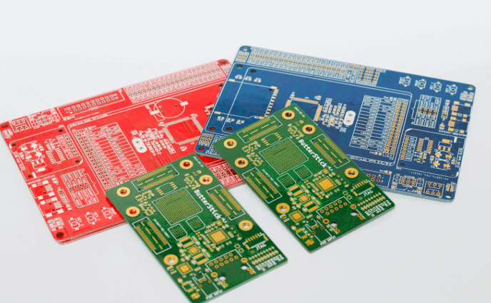
Looking for a reliable PCB manufacturer in Iraq? This blog will introduce the pain points of Iraq PCB manufacturing and how EBest Circuit(Best Technology) solve these problems.
Growing demand for reliable electronic components in Iraq has made professional PCB manufacturer in Iraq services increasingly vital. From infrastructure projects to industrial automation, high-quality PCB solutions act as a key enabler for operational efficiency. As a trusted PCB manufacturing partner serving Iraq, EBest Circuit(Best Technology) understand the unique market dynamics and local requirements, offering tailored services that bridge the gap between global manufacturing standards and regional needs. Whether you need small-batch prototyping or large-scale production, partnering with a reputable PCB manufacturer in Iraq ensures consistent quality and timely delivery for your critical applications.
Are You Facing the Following Challenges in Your PCB Project?
- Do frequent delays in PCB prototyping and production disrupt your project timelines, especially when dealing with local Iraq PCB suppliers?
- Is the quality of PCB products inconsistent, with issues like board warping, solder defects, or poor conductivity affecting your final products?
- Lack of professional support in PCB design optimization, leading to unnecessary material waste and increased production costs?
- Struggle to find a PCB partner that can handle urgent orders and ensure on-time delivery amid Iraq’s complex logistics environment?
- Concerned about assembly defects such as component misalignment or poor solder joints that compromise product reliability?
End-to-End Assurance from Requirement to Delivery
- Customized Production Planning: We conduct in-depth demand analysis to create personalized production schedules, avoiding delays by integrating flexible manufacturing processes and proactive supply chain management.
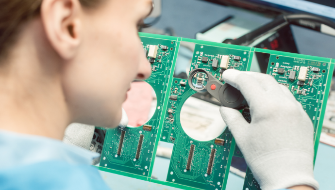
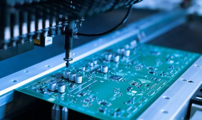
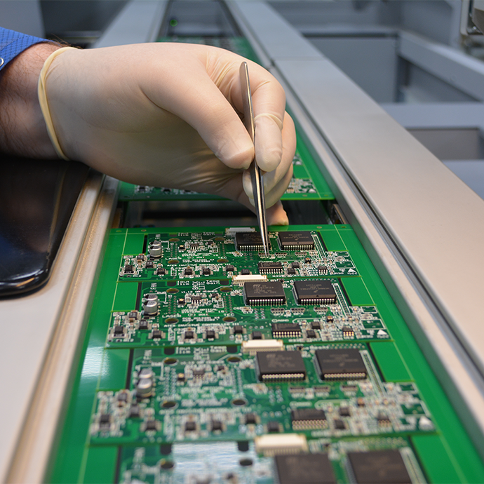
- Strict Quality Control System: Implement full inspection for mass production, combining advanced AOI and X-Ray testing equipment to eliminate defects like board warping and solder issues, ensuring consistent product quality.
- Professional Design Support: Provide free DFM analysis to optimize your PCB design, reduce material waste, and improve production feasibility while controlling costs.
- Urgent Order Response Mechanism: 24-hour rapid prototyping service and 99.2% on-time delivery rate, supported by optimized logistics solutions tailored to Iraq’s transportation characteristics to meet your tight deadlines.
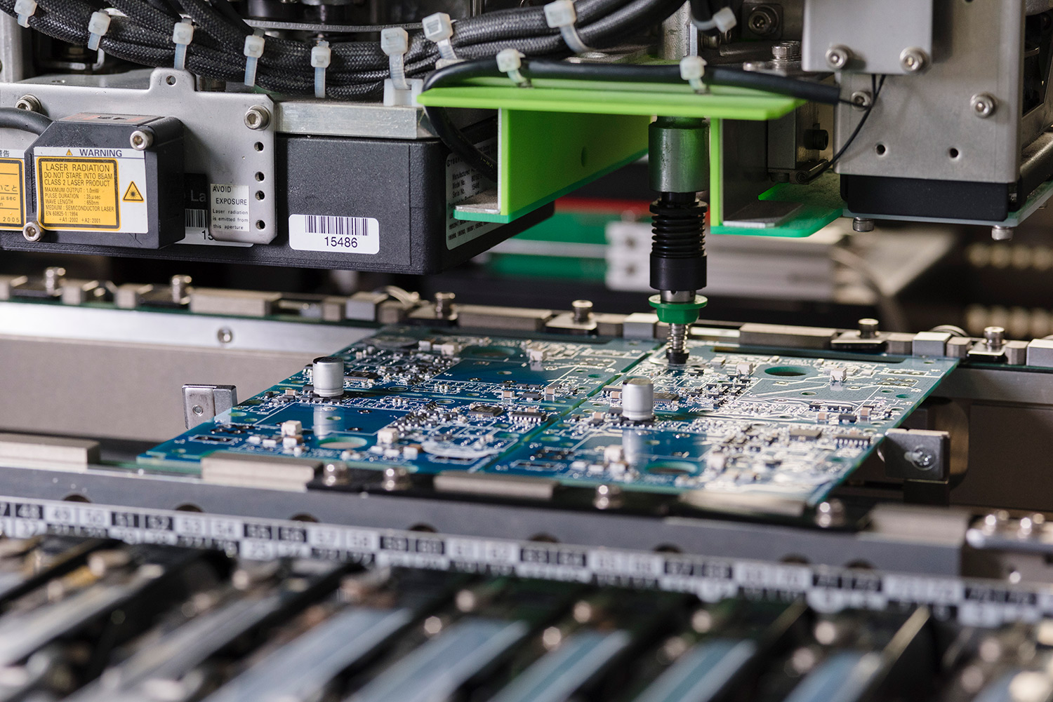
- Precision Assembly Process: Adopt standardized assembly procedures, strict solder paste printing control, and reflow soldering parameter optimization to minimize component misalignment and poor solder joint issues.
Why Iraq Clients Choose EBest Circuit(Best Technology) for PCB Manufacturer?
- 19 Years of Production Experience: With 19 years in the PCB manufacturing industry, we have rich experience in solving complex production problems and can help you reduce costs and improve efficiency.
- Free DFM Analysis: Provide free design for manufacturability analysis to identify potential issues in your design early, ensuring smooth production and reducing rework costs.
- Complete Certification Portfolio: Hold ISO9001:2015, ISO13485:2016, REACH, RoHS, and IATF16949 certifications, meeting the quality and compliance requirements of various industries in Iraq.
- Competitive Pricing: As a professional Iraq PCB Manufacturer, we leverage bulk material procurement and optimized production processes to offer competitive prices without compromising quality.
- Cost-Sensitive Solutions: Customize cost-saving plans based on your project requirements, optimizing design and material selection to reduce overall production costs.
- 24-Hour Rapid Prototyping: Efficiently respond to urgent orders with 24-hour turnaround for PCB prototyping, accelerating your product development cycle.
- High On-Time Delivery Rate: Boast a 99.2% on-time delivery rate, supported by a mature supply chain and customized logistics solutions for Iraq’s market to ensure timely order fulfillment.
- Superior Quality Assurance: Implement full inspection for mass production with a strict quality control process covering material incoming, production process, and finished product testing to ensure product reliability.

Our Professional Iraq PCB Design Services: Free DFM & Technical Support
As a trusted Iraq PCB company partner, our design services are centered on two core advantages: free DFM (Design for Manufacturability) analysis and professional technical support. These services directly address key pain points in the design process, delivering tangible value to your projects.
Our free DFM analysis acts as a proactive quality gate for your designs. We identify potential flaws early such as unreasonable component spacing, improper pad layout or non-compliant line widths which are prone to causing production issues. By optimizing these aspects, we enhance product reliability while cutting down rework costs and material waste significantly.
Backed by 19 years of industry experience, our comprehensive technical support covers the entire design lifecycle. We provide end-to-end assistance from design optimization to full custom design solutions, ensuring every design meets Iraq’s local regulations and global industry standards. This professional guidance guarantees seamless manufacturability and market acceptance for your products, all at no additional cost.
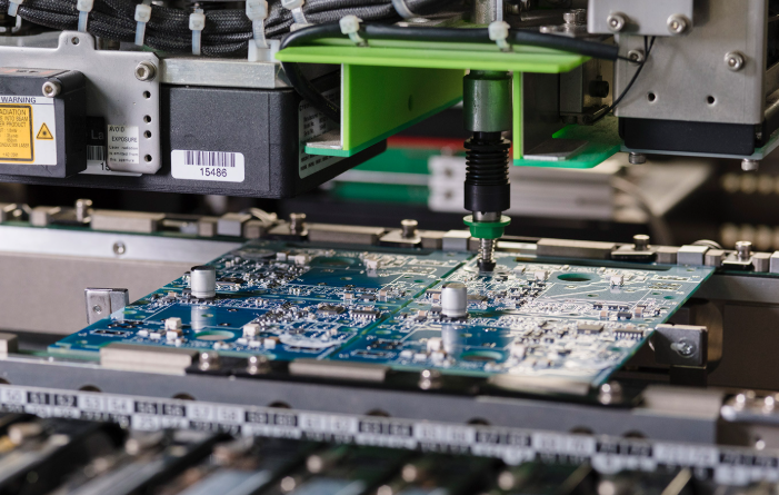
Our Iraq PCB Prototyping Services: Fast Delivery & Reliable Quality
As a professional PCB Manufacturer in Iraq focus partner, we are not a local PCB producer but specialize in providing high-efficiency prototyping services tailored for Iraq’s market needs. Our core advantage lies in ultra-fast lead times, with 24-hour rapid prototyping and delivery as our key commitment to you.
We realize that urgent project schedules demand timely prototyping support. Our 24-hour rapid prototyping service ensures test-ready PCBs are delivered within one business day, eliminating long waiting periods and accelerating your project progress. This speed is backed by our advanced production lines and dedicated urgent order response team, which prioritize your prototyping needs to meet tight deadlines.
While emphasizing speed, we never compromise on quality. Our Iraq PCB prototyping service uses cutting-edge high-precision equipment to ensure pinpoint accuracy in line widths and hole positions. Every prototype undergoes strict multi-stage inspections, including AOI and X-ray testing, to fully comply with your specifications. We also have optimized logistics solutions for Iraq, ensuring that even as a non-local provider, our 24-hour prototyping delivery commitment is reliably fulfilled. Whether it’s simple single-layer boards or complex multi-layer PCBs, our fast and high-quality prototyping services fully support your diverse project requirements.

Our Lead Time for Prototyping
| Layers | Normal Service | Fastest Service |
| 1 | 7 Days | 24 H |
| 2 | 8 Days | 24 H |
| 4 | 10 Days | 48 H |
| 6 | 10 Days | 72 H |
| 8 | 12 Days | 72 H |
| ≥10 | TBD | TBD |
Case Studies of Our Iraq PCB Project
Project Background: An Iraq cement plant needed high-reliability PCB products for its DCS (Distributed Control System), the core of its automated production line, and its ongoing smart upgrade also required these PCBs to support stable data transmission and equipment control to avoid production interruptions.
Requirements: The PCBs were required to withstand 120℃ sustained high temperatures in the kiln area and resist heavy dust, while also needing urgent delivery within 7 days to prevent production downtime with zero tolerance for performance failures in the harsh industrial environment.
Difficulties: The high-temperature and high-dust environment of the cement plant easily caused PCB warping and solder joint corrosion, while Iraq’s complex logistics and customs clearance processes posed risks to the 7-day urgent delivery timeline; additionally, the DCS system required ultra-low error rates for PCB line width and hole position.
Our Solutions:
- Material selection: Selected FR-4 high-Tg (170℃) material for thermal stability, matched with enhanced solder mask and sealed edge treatment to achieve dust resistance.
- Design optimization: Conducted free DFM analysis to adjust line spacing and pad layout, improving dust-proof performance and reducing signal interference.
- Urgent production: Activated 24-hour rapid prototyping service to complete sample validation in 1 day, then arranged a dedicated production line for mass production.
- Logistics guarantee: Cooperated with local trusted logistics partners in Iraq to customize door-to-door delivery, completing customs clearance in advance to meet the 7-day deadline.
Output Results: The delivered PCBs passed 100-hour high-temperature dust chamber testing with zero performance anomalies, were delivered 12 hours ahead of the 7-day schedule to ensure uninterrupted production line operation, and maintained stable operation for over 6 months with a 0% failure rate after installation, leading the customer to sign a 2-year long-term supply contract with our PCB Manufacturer in Iraq.
FAQ of Iraq PCB Manufacturing
Q1: How to solve the problem of delayed PCB delivery caused by complex logistics in Iraq?
A1: We cooperate with local reliable logistics partners in Iraq to customize multi-modal transportation schemes. We also strictly abide by PSP compliance requirements to ensure smooth customs clearance. With real-time logistics tracking and 99.2% on-time delivery rate, we effectively avoid delivery delays.
Q2: What measures are taken to ensure the quality of PCB products in mass production?
A2: Our PCB Manufacturer in Iraq implements full inspection in mass production. We use advanced AOI and X-Ray testing equipment to inspect each PCB, covering solder joints, line width, and hole position accuracy. Strict quality control processes from material incoming to finished product delivery ensure stable product quality.
Q3: Can you provide support for optimizing PCB design to reduce production costs?
A3: Yes, we provide free DFM analysis services. Our professional team will optimize your design from the perspective of manufacturability, such as reasonable layout and material selection, to reduce material waste and rework costs, achieving cost savings under the premise of ensuring performance.
Q4: How to meet the demand for urgent PCB prototyping orders?
A4: We have a dedicated urgent order response team and 24-hour rapid prototyping equipment. For urgent prototyping orders, we can complete sample production and delivery within 24 hours, helping you accelerate product development and testing progress.
Q5: Do your PCB products meet the compliance requirements of Iraq’s local market?
A5: Yes, our PCB products hold multiple international certifications including ISO9001:2015, ISO13485:2016, REACH, RoHS, and IATF16949. We fully understand Iraq’s local industry regulations and can ensure that our products meet the relevant compliance requirements of the Iraqi market.