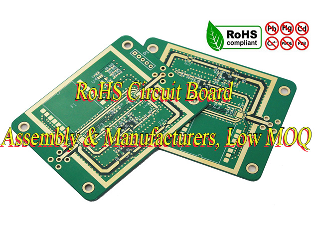
Why choose RoHS circuit board? Let’s discover its benefits, applications, compliant standard, design considerations, assembly process, Identification methods for RoHS PCB board.
Are you worried about these problems?
- High RoHS compliance design costs, budget hard to control?
- Slow prototyping for urgent projects, RoHS testing unable to keep up?
- Unstable RoHS indicators in mass production, quality hard to guarantee?
As a RoHS circuit board manufacturer, EBest Circuit (Best Technology) can provide you service and solutions:
- Cost Optimization: Leverage 19 years of RoHS material database and intelligent design to reduce costs by 15%-20% at the source, ensuring compliance without exceeding budgets.
- Rapid Prototyping: Complete 24-hour prototyping with full RoHS testing, real-time report sync, zero wait for validation.
- Quality Assurance: 100% full inspection + AI verification, indicator deviation <0.08%, cloud-traceable data, worry-free mass production.
Welcome to contact us if you have any request for RoHS circuit board: sales@bestpcbs.com.
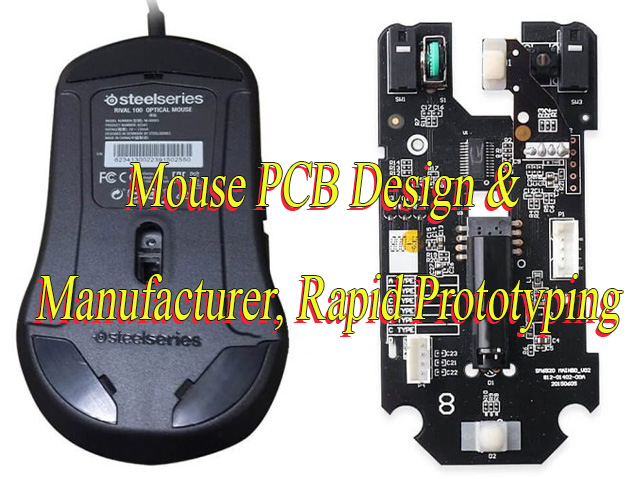
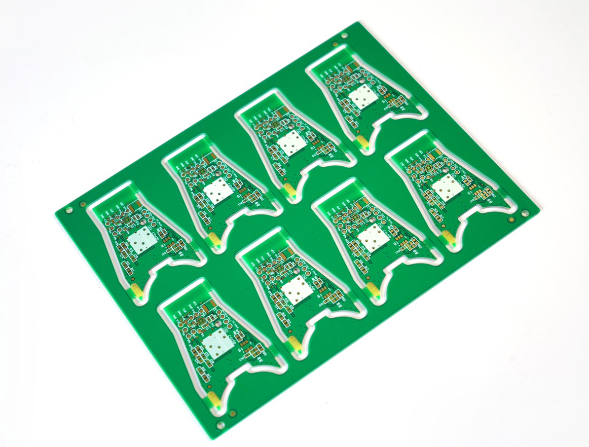
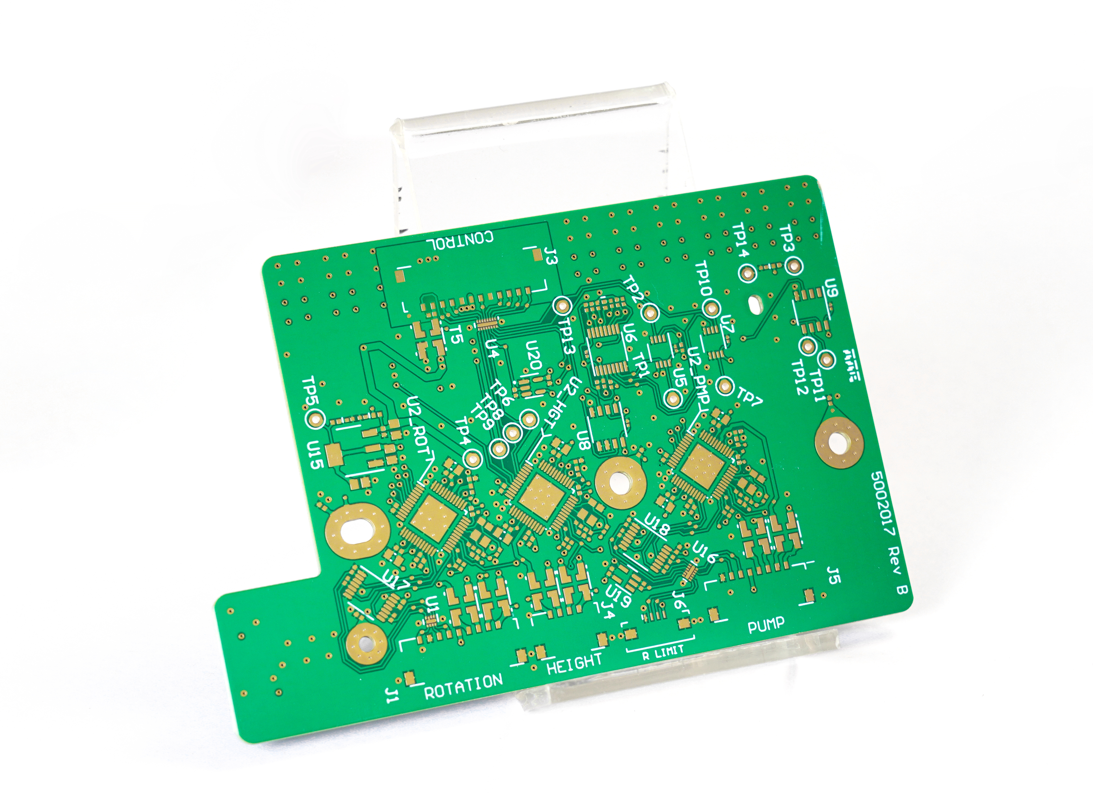
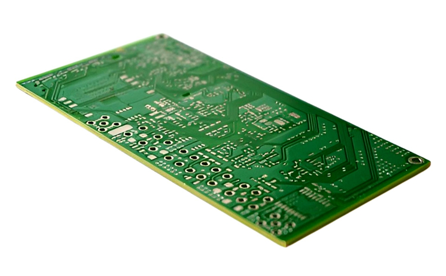
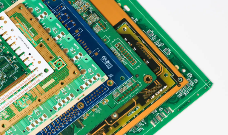
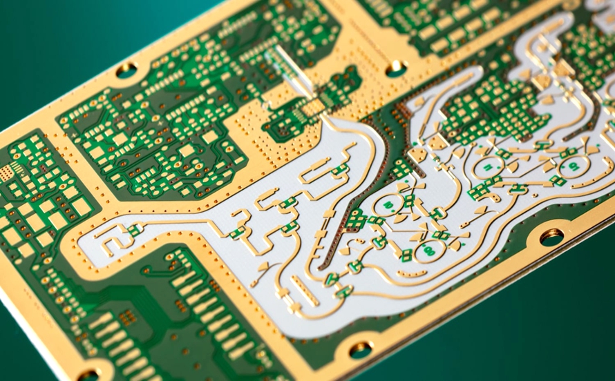
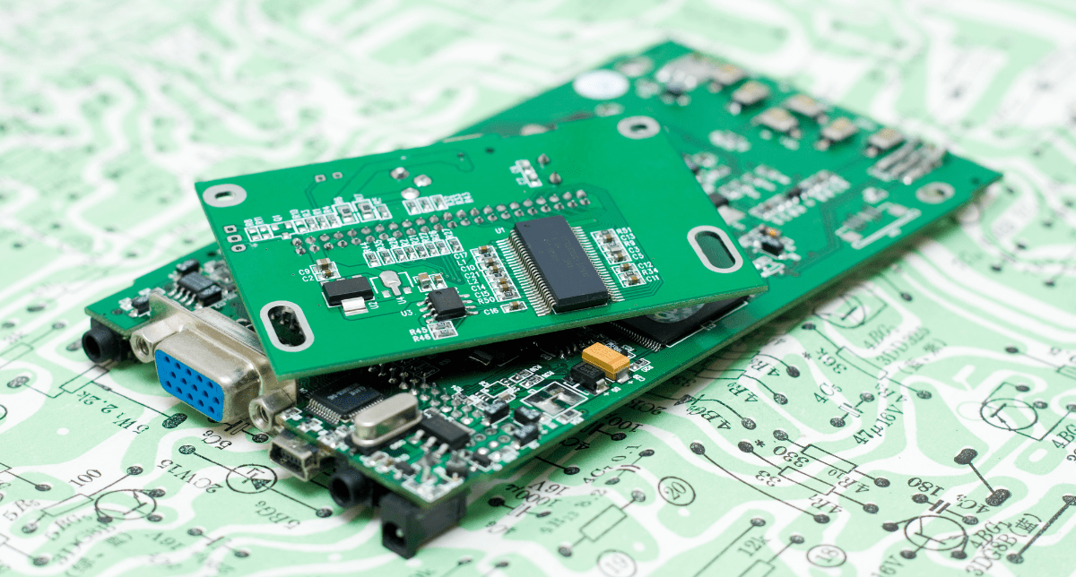
What Is RoHS Circuit Board?
RoHS Circuit Board refers to a printed circuit board compliant with the EU’s Restriction of Hazardous Substances Directive (latest RoHS 3). Its core requirement mandates that in homogeneous materials of the board, the content of 10 hazardous substances, including lead (Pb), mercury (Hg), cadmium (Cd), and hexavalent chromium (Cr6+), must remain below statutory limits (e.g., lead, mercury, and hexavalent chromium ≤0.1%; cadmium ≤0.01%).
Achieved through lead-free soldering (e.g., SAC305 alloy), halogen-free substrates, and eco-friendly surface treatments, this ensures electronic products do not pollute the environment post-disposal. It serves as a mandatory environmental compliance threshold for entering the EU and global mainstream markets.
What Are Advantages of RoHS PCB Boards?
Advantages of RoHS PCB Boards:
- Market Access and Compliance: RoHS certification is a mandatory requirement in markets like the EU. Uncertified products cannot enter the market and may be detained or fined. For example, the EU RoHS Directive requires that electrical and electronic equipment comply with the Restriction of Hazardous Substances Directive, otherwise they are prohibited from sale.
- Reducing Legal Risk: RoHS compliance can avoid fines, product recalls, or legal action. For example, the EU imposes strict penalties for non-compliant products, such as hefty fines and product returns.
- Enhancing Brand Image and Consumer Trust: Environmental certification aligns with international consumer preferences for sustainable products, enhancing brand reputation. For example, EU consumers are more inclined to purchase environmentally friendly products, making RoHS certification a “green business card.”
- Supply Chain Optimization and Cost Control: Reducing waste disposal costs through environmentally friendly supply chain management can potentially reduce material costs in the long term. For example, the large-scale application of environmentally friendly materials can reduce costs and enhance competitiveness.
- Technological Innovation and Product Upgrades: RoHS promotes the development of lead-free solder and environmentally friendly materials, improving product performance such as high-temperature resistance and corrosion resistance, and extending product life.
- Facilitating International Trade: RoHS certification simplifies customs clearance, reduces tariffs and trade barriers, and promotes cross-border cooperation. For example, many international buyers require suppliers to have RoHS certification to facilitate cooperation.
- Adapting to global environmental trends: Many countries have adopted similar regulations to RoHS, making it easier for certified products to enter other markets, such as China and Japan, and expand market share.
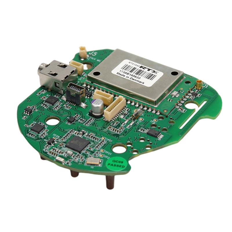
What Are Applications of RoHS Circuit Board?
Applications of RoHS Circuit Boards:
- Consumer Electronics: Mobile phones, tablets, laptops, TVs, digital cameras, Bluetooth headsets.
- Home Appliances: Refrigerators, washing machines, air conditioners, microwaves, vacuum cleaners, toasters, LED lighting fixtures.
- Automotive Electronics: In-car entertainment systems, ECUs (Electronic Control Units), sensors, wiring harnesses, battery management systems.
- Medical Devices: Blood pressure monitors, blood glucose meters, X-ray machines, ultrasound equipment, cardiac pacemakers.
- Industrial Control & Automation: PLCs (Programmable Logic Controllers), industrial robots, sensors, motor drives, automation production line control boards.
- Communication Equipment: Routers, switches, 5G base stations, fiber-optic communication modules, telephone exchanges.
- Lighting Devices: LED lamps, smart lighting systems, energy-saving bulbs, fluorescent tubes.
- Toys & Children’s Products: Electronic toys, game controllers, remote-controlled cars, smart educational devices.
- Green Energy & Renewables: Solar inverters, wind energy controllers, energy storage systems, smart grid equipment.
- Aerospace & Military Equipment: Satellite communication devices, military radars, aerospace electronic systems.
RoHS Circuit Board Compliant Standard
| Element Category | Specific Content |
| International Standard Reference | RoHS 3 (EU Directive 2015/863) |
| Restricted Hazardous Substances | Lead (Pb), Cadmium (Cd), Mercury (Hg), Hexavalent Chromium (Cr⁶⁺), Polybrominated Biphenyls (PBB), Polybrominated Diphenyl Ethers (PBDE), Phthalates (DEHP, BBP, DBP, DIBP) |
| Maximum Concentration Limits | Cadmium (Cd) ≤ 0.01% (100 ppm); Other 9 substances ≤ 0.1% (1000 ppm) (measured in homogeneous materials) |
| Scope of Application | All electrical and electronic equipment (EEE) placed on the EU market, covering 11 categories. Global regulations such as China RoHS and California SB 20/50 (USA) are highly similar or based on EU RoHS |
| Homogeneous Material Definition | The level of a single material that cannot be mechanically separated into different materials |
| Technical Documentation Requirements | Technical Construction File (TCF) and Declaration of Conformity (DoC) must be prepared and retained as proof of RoHS compliance |
| Exemption Clauses | Exemption lists exist for specific applications or materials (e.g., lead in high-temperature soldering). Continuous monitoring of EU Official Journal updates is required |
| Testing Standards Reference | IEC 62321 series (preferred standard for hazardous substance testing), EN 14372 (phthalates), etc. |
| Supply Chain Management | Establish a hazardous substance control system in the supply chain, systematically collect and verify suppliers’ compliance declarations and test reports |
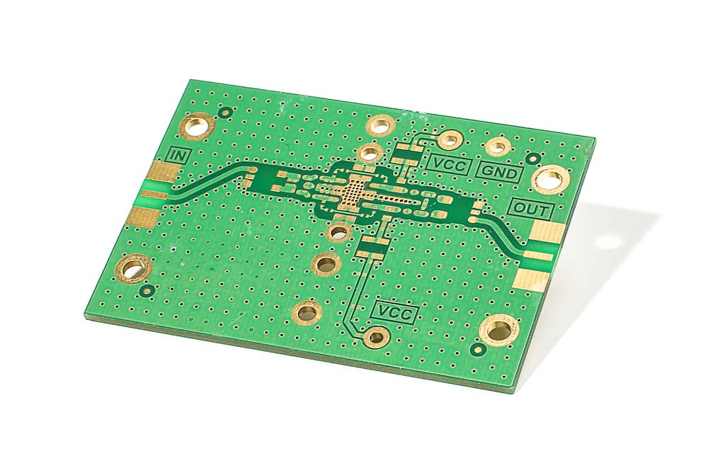
RoHS Circuit Board Design Considerations
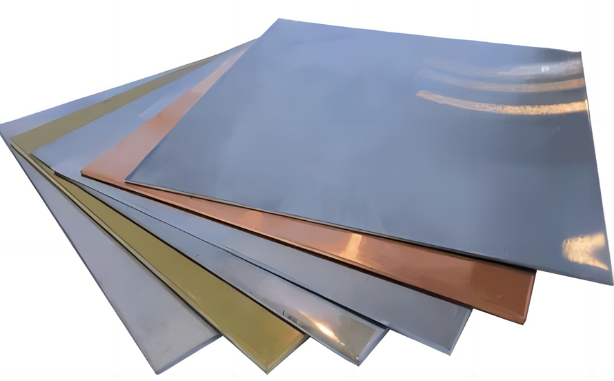
Environmental-Friendly Substrate Parameter Selection Strategy
- Halogen-Free Substrate Design Adaptation: Prioritize IEC 61249-2-21 certified halogen-free FR-4 materials, requiring suppliers to provide chlorine/bromine content reports (<900ppm). Verify Tg ≥170℃ to withstand 260℃ peak temperature in lead-free SMT processes. Conduct TMA testing to match substrate CTE with copper foil and solder, preventing delamination or via cracking post-soldering.
- Material Optimization for High-Frequency/High-Power Scenarios: For high-frequency PCBs, select PTFE/ceramic substrates to minimize signal loss (Dk=2.9~3.2, Df=0.002~0.005). For high-power applications, adopt aluminum/copper substrates with thermal conductivity ≥1.5W/mK. Utilize 3D thermal modeling in design tools (e.g., Altium Designer) to simulate heat dissipation paths.
Lead-Free Soldering Compatibility Design Essentials
- Pad and Via Design Specifications: When using SnAgCu (e.g., SAC305) solder, increase pad size by 10-15% to compensate for reduced wettability. For via-in-pad designs, reinforce solder mask thickness (≥0.1mm) to prevent solder wicking. Optimize via placement to mitigate thermal stress from lead-free solder expansion.
- Surface Finish Selection Based on Application: Choose ENIG for high-frequency/fine-pitch devices (BGA), maintaining Ni 3-5μm/Au 0.05-0.1μm layers. For short-lifecycle products, select OSP with validated solderability retention (>6 months). Exclude leaded finishes entirely.
Solder Mask and Legend Ink Compliance Standards
- Solder Mask Selection Criteria: Use RoHS-compliant water-based or UV-curable solder masks, passing 260℃/10-reflow tests with adhesion ≥5B (ASTM D3359). Specify heavy metal content: Pb/Cd <1000ppm (Cd<100ppm). Verify compatibility with substrate CTE through thermal cycling tests.
- Legend Ink Environmental Requirements: Employ lead-free legend inks resistant to high humidity/temperature (85℃/85%RH/1000h). Avoid phthalate-containing inks, complying with REACH SVHC restrictions. Ensure legibility under harsh conditions.
Design-Stage Environmental Compliance Verification
- Simulation and Testing Protocols: Validate thermal distribution via thermal simulation (e.g., ANSYS Icepak) to prevent hotspots under lead-free soldering conditions. Verify signal integrity metrics (±10% impedance control, <5% crosstalk) through HyperLynx simulations.
- Material Traceability in Design Documentation: Annotate environmental material specifications (substrate model, surface finish, solder mask type) in Gerber files. Establish BOM-design document linkage for traceability to compliance reports.
Reliability Enhancement Design Strategies
- Thermal-Mechanical Stress Mitigation: Optimize layout to reduce thermal concentration in high-density areas. Implement thermal via arrays and BGA thermal pads connected to internal planes to dissipate heat. Adjust solder mask thickness and via spacing based on accelerated life test results (thermal cycling: -40℃~125℃/1000 cycles; humidity: 85℃/85%RH/1000h; salt spray: 5% NaCl/96h).
RoHS Compliant Circuit Board Assembly Process
1. Material Preparation & Compliance Verification
- Lead-Free Solder Selection: Use Sn-Ag-Cu (SAC305) or Sn-Bi solder paste/wire with Pb ≤0.1%, certified by IEC 62321.
- Flux & Cleaning Agents: Adopt halogen-free no-clean flux (e.g., rosin-based) and water-based cleaners compliant with REACH (pH 7-9); prohibit CFC/trichloroethylene.
- Component Pre-Screening: Validate RoHS declarations, MSDS, and XRF test results for components (e.g., ENIG/OSP surface finishes).
2. PCB Pretreatment & Solder Paste Printing
- PCB Baking: Bake moisture-sensitive PCBs at 120°C for 4 hours to prevent soldering delamination; ensure surface finishes (e.g., ENIG) withstand ≥260°C.
- Printing Parameters: Use 304 stainless steel stencil (0.1-0.15mm thickness), print speed 20-50mm/s, squeegee pressure 0.2-0.4MPa. SPI verifies paste thickness (0.12-0.18mm) and alignment (≤±15μm).
- Nitrogen Protection: Inject 99.99% N₂ in printing/reflow ovens to reduce oxidation and enhance wettability.
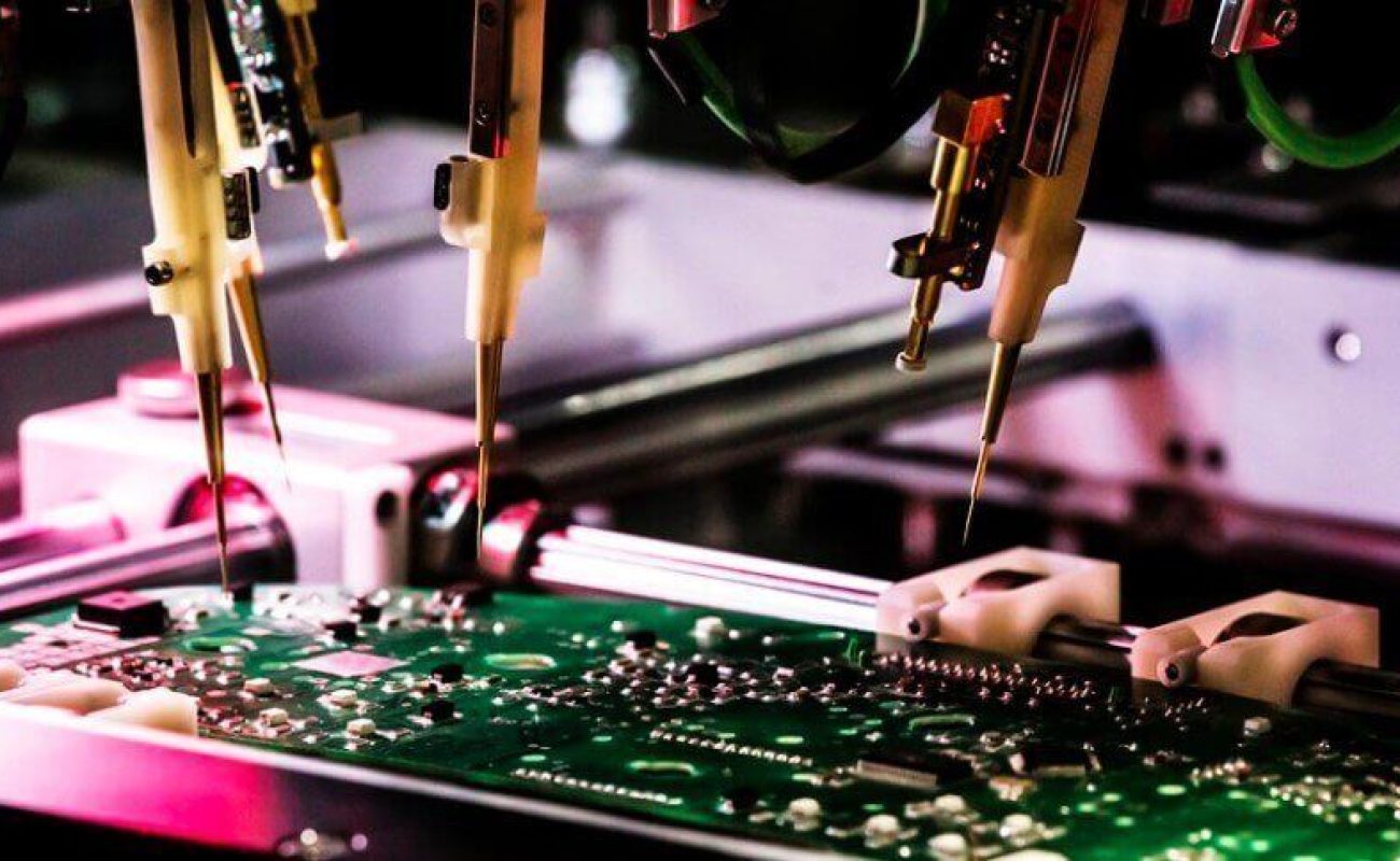
3. Surface Mount Technology (SMT) Process
- Placement Accuracy: High-precision pick-and-place machines (±0.05mm) handle 01005 components via vision alignment; BGA/QFN devices require preheating to ≥150°C.
- Reflow Profile:
- Preheat Zone: 150-180°C (1-3°C/s ramp), 90-120s duration for flux activation.
- Reflow Zone: Peak 235-245°C (SAC305 melting point 217°C), 60-90s above liquidus.
- Cooling Zone: ≤4°C/s slope to avoid thermal shock.
- AOI Inspection: Automated Optical Inspection detects defects (e.g., bridges, tombstoning) with ≤50ppm failure rate; X-Ray checks BGA voids (≤20%).
4. Through-Hole Technology (THT) & Wave Soldering
- Component Preparation: Bend leads at 45-60° for long-pin devices; maintain height tolerance (±0.2mm).
- Soldering Parameters: Solder bath temperature 250-260°C, immersion time 3-5s; adjust wave height (1/2-2/3 board thickness) and angle (5-10°). Nitrogen protection ensures smooth solder fillets without cold joints.
- Trimming & Cleaning: Cut leads to 2-3mm; no-clean processes proceed to testing; water-based cleaning uses 40-50°C for 2-3min to avoid corrosion.
5. Post-Soldering & Rework
- Manual Soldering: Use temperature-controlled irons (350-380°C) with lead-free wire and no-clean flux; limit soldering time to ≤3s.
- Rework Guidelines: BGA rework employs hot air guns (150°C preheat/235°C reflow) with X-Ray verification; QFN devices require precision hot air + tweezers.
6. Inspection & Functional Testing
- ICT Testing: In-circuit tests verify electrical connections (open/short detection) with ±0.1% accuracy.
- FCT Verification: Functional tests simulate real-world conditions (e.g., power/signal integrity); aging tests (40°C/48h) screen early failures.
- RoHS Re-Testing: XRF fluorescence analysis (heavy metals) and ICP-OES/MS quantification ensure compliance with EU/China RoHS limits.
7. Packaging & Traceability
- ESD Packaging: Use conductive bags/foam or moisture-barrier bags labeled “RoHS Compliant” and CE mark.
- Batch Traceability: Record production date, supplier data, and test results for recall management.
- Compliance Documentation: Include RoHS declarations, test reports, and MSDS with shipments for customer audits.
How to Identify and Verify RoHS Circuit Boards?
1. RoHS Compliance Marking Identification
- Verify presence of “RoHS compliant” or CE marking (with RoHS Declaration of Conformity) on product body, packaging, or accompanying documentation. EU products must display CE mark concurrently. Markings must be legible, durable, and traceable to specific production batches.
2. Material Declaration and Conformity Documentation Review
- Require manufacturers to provide Materials Declaration (MD) or Declaration of Conformity (DoC) specifying chemical compositions of components. Confirm compliance of hazardous substances including lead (≤1000ppm), cadmium (≤100ppm), mercury, hexavalent chromium, PBB, and PBDE. Validate document authenticity through issuance date, manufacturer details, and third-party certification numbers.
3. Laboratory Testing Verification Protocol
- Utilize X-ray fluorescence spectrometer (XRF) for non-destructive testing of metal content in circuit boards. For critical components like solder joints and connectors, employ wet chemical analysis or inductively coupled plasma mass spectrometry (ICP-MS) for precise quantification. Sampling must cover substrates, solder materials, surface coatings, and compare results with manufacturer data. Non-conformances trigger supplier or process traceability audits.
4. Supply Chain and Manufacturing Process Audit
- Verify supplier ISO 14001 certification and RoHS compliance processes. Inspect solder materials for lead-free alloys (e.g., Sn-Ag-Cu), surface treatments using trivalent chromium instead of hexavalent chromium, and cleaning/flux agents free of prohibited substances. Confirm dedicated equipment for lead-free processes to prevent cross-contamination. Audit batch records and operational signatures for traceability.
5. Regulatory Updates and Third-Party Certification Monitoring
- Regularly monitor RoHS regulation updates (e.g., RoHS 3 phthalate restrictions) via EU Commission official channels or authoritative agency bulletins. Require manufacturers to provide annual third-party certification reports (e.g., UL, T?V) or verify EU conformity assessment database records for product registration compliance.
6. Alternative Material and Process Risk Assessment
- Evaluate safety risks of lead-free solders and halogen-free flame retardants. Validate circuit board reliability through thermal cycling and high-temperature/humidity testing. Review supplier stability data and failure analysis reports for alternative materials. Confirm no adverse impact on electrical conductivity, thermal resistance, or other performance metrics. Pilot small-batch production for verification if necessary.
7. End-of-Life Handling Requirements
- Check for recycling symbols (e.g., WEEE mark) and disassembly instructions with hazardous substance separation guidance. Verify recycling channels meet RoHS disposal standards to ensure safe handling of toxic materials in waste circuit boards, preventing environmental contamination.
Why Choose EBest Circuit (Best Technology) as RoHS Circuit Board Manufacturers?
Reasons Why Choose Us as RoHS Circuit Board Manufacturer:
Competitive Pricing Strategy:
- Utilizing a 19-year production error database and intelligent material ratio systems, cost-sensitive designs are precisely executed. Each circuit board employs RoHS-certified eco-friendly materials, reducing material costs by 15%-20% compared to conventional solutions. ISO 9001 process optimization ensures bulk production pricing advantages, enhancing client product market competitiveness.
24-Hour Rapid Prototyping for Urgent Orders:
- Leveraging intelligent production lines and dedicated RoHS testing pathways, urgent orders achieve 24-hour rapid prototyping. Samples undergo comprehensive inspection to meet RoHS 2.0 standards, enabling clients in high-compliance sectors like medical and automotive electronics to accelerate market entry and reduce product launch timelines by over 30%.
99.2% On-Time Delivery Guarantee
- Adopting IATF 16949 automotive-grade production management and intelligent scheduling systems, 99.2% of orders are delivered on schedule. Each batch includes RoHS test reports, ensuring dual assurance of environmental compliance and stable lead times while minimizing client supply chain risks.
100% Full Inspection Quality Control System
- Bulk production implements 100% full inspection standards, integrating Six Sigma quality control processes with AI visual inspection systems to maintain defect rates below 0.08%. Every circuit board passes RoHS-specific verification, ensuring zero environmental compliance risks for medical-grade and automotive-grade products.
Authoritative Certification Credentials
- Holding ISO 9001 quality management, IATF 16949 automotive standards, medical ISO 13485, and RoHS certification, forming a quadruple international certification barrier. Certificates are traceable, assisting clients in meeting global market environmental access requirements such as EU and North American regulations.
Free DFM Design Optimization
- Complimentary DFM analysis services provided by senior engineering teams optimize designs in conjunction with RoHS material characteristics. Through solderability testing and thermal design simulations, mass production risks are reduced, achieving over 99.5% yield rates.
Customized Cost Optimization Solutions
- Based on client product characteristics and market positioning, full-chain cost optimization solutions are developed by integrating the RoHS-compliant material library with intelligent quoting systems. Alternative material testing and process improvements achieve dual objectives of cost reduction and environmental compliance, maximizing client profitability.
Welcome to contact us if you have any request for RoHS circuit board: sales@bestpcbs.com.