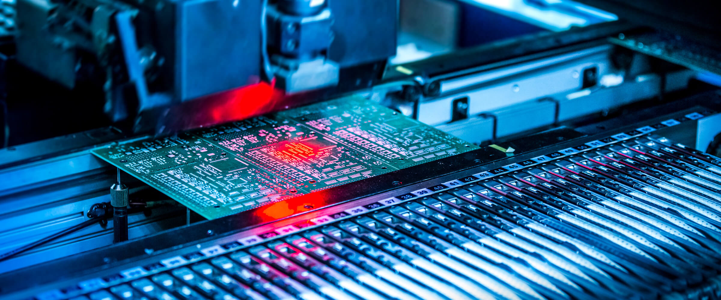
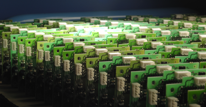
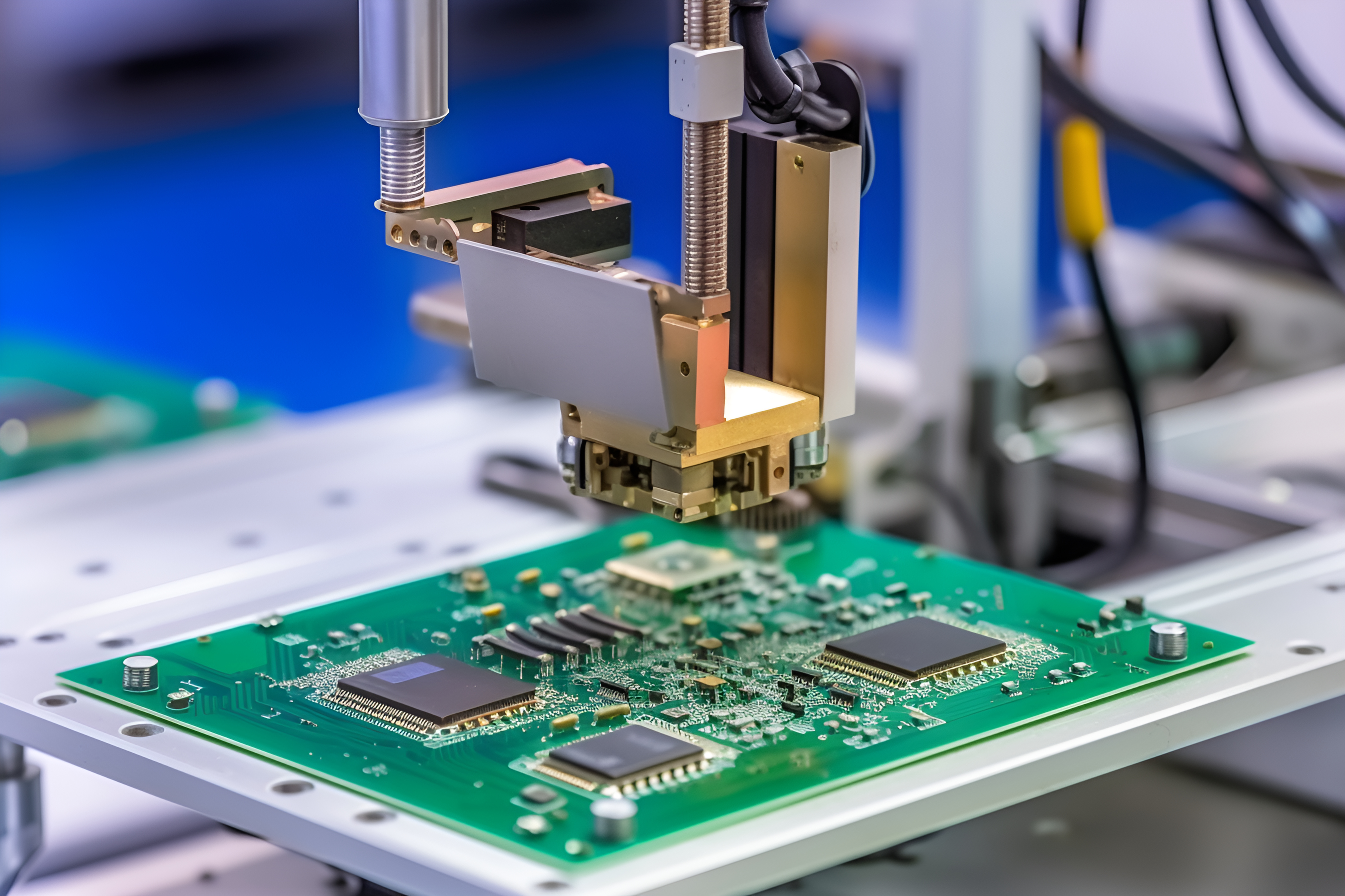
Circuit card assemblies sit at the core of modern electronics. A circuit card assembly is a printed circuit board that has been fully populated with electronic components and soldered into place. Once assembled, it becomes a working unit capable of controlling power, processing signals, and enabling communication within an electronic device.
What Is a Circuit Card Assembly?
A circuit card assembly, often shortened to CCA, is a printed circuit board that has electronic components mounted and connected to it. These components are not loose. They are fixed, soldered, and electrically linked according to a design.
The circuit card assembly definition focuses on function. It is not just a board with copper paths. It is a working electronic unit. Once assembled, it can process signals, control power, or manage data.
Many people use the term printed circuit board assembly in the same way. In daily use, they often mean the same thing. Still, some industries prefer “circuit card assembly” because it highlights the complete, functional state.
A bare board cannot do anything alone. A circuit card assembly can. This is why CCAs are central to electronics manufacturing.
What Are the Main Components of a Circuit Card Assembly?
A circuit card assembly is a system. Every part plays a role. Each component adds a specific function, and together they create reliable operation.
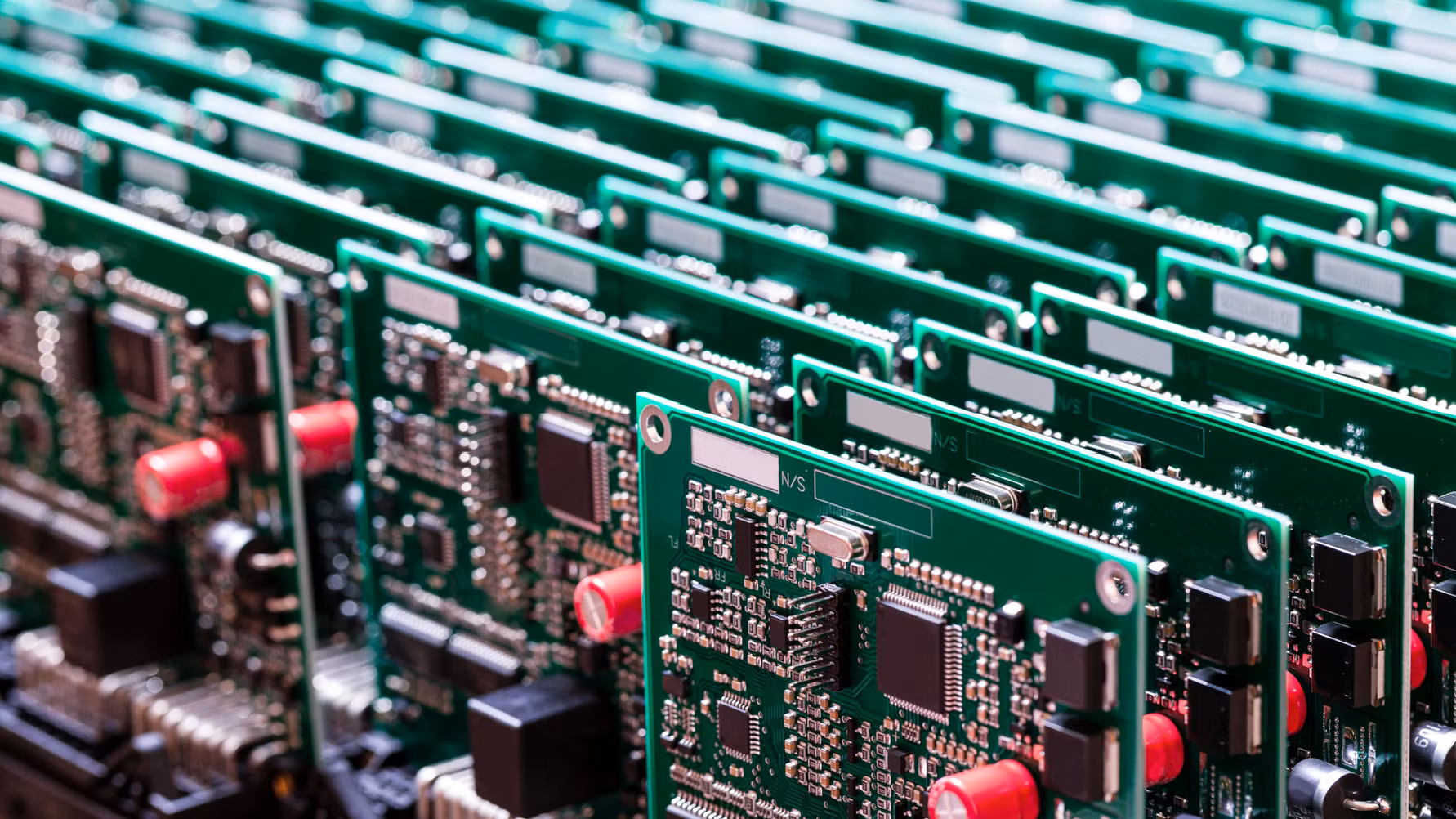
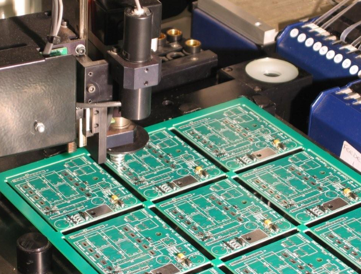
- The Printed Circuit Board: The printed circuit board is the foundation. It is usually made from fiberglass material like FR-4. Copper layers form electrical paths on the surface or inside the board. The board provides structure. It also controls signal flow.
- Passive Components: Passive parts include resistors, capacitors, and inductors. These components shape current and voltage. They store energy, limit flow, or filter noise.
- Active Components: Active components bring intelligence. These include microcontrollers, processors, and integrated circuits. They process signals. They make decisions. They control outputs.
- Connectors and Interfaces: Connectors link the assembly to other systems. They allow power input, data transfer, or mechanical connection.
- Solder Materials: solder joints connect everything. The quality of solder paste, reflow profile, and inspection determines long-term stability. A strong joint survives vibration and heat.
Each component matters. Together, they turn a simple board into a reliable circuit card assembly.
What Are the Different Types of CCA Assembly?
Different products need different assembly styles. Choosing the right type affects cost, size, and performance.
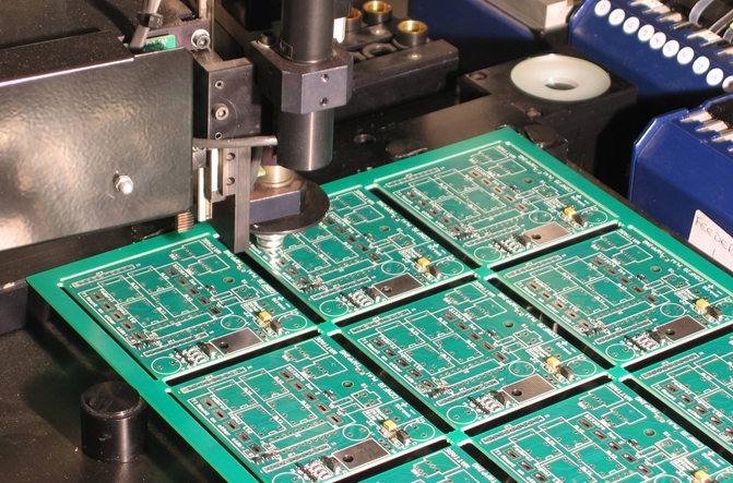
Through-Hole Assembly
Through-hole assembly uses components with long leads. These leads pass through holes in the board and are soldered on the opposite side.
This method offers strong mechanical bonds. It works well for large components and connectors. However, it takes more space. It also increases labor.
Surface Mount Assembly
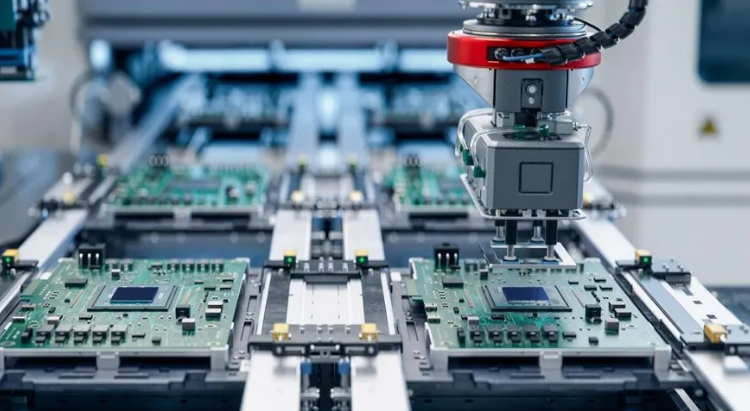
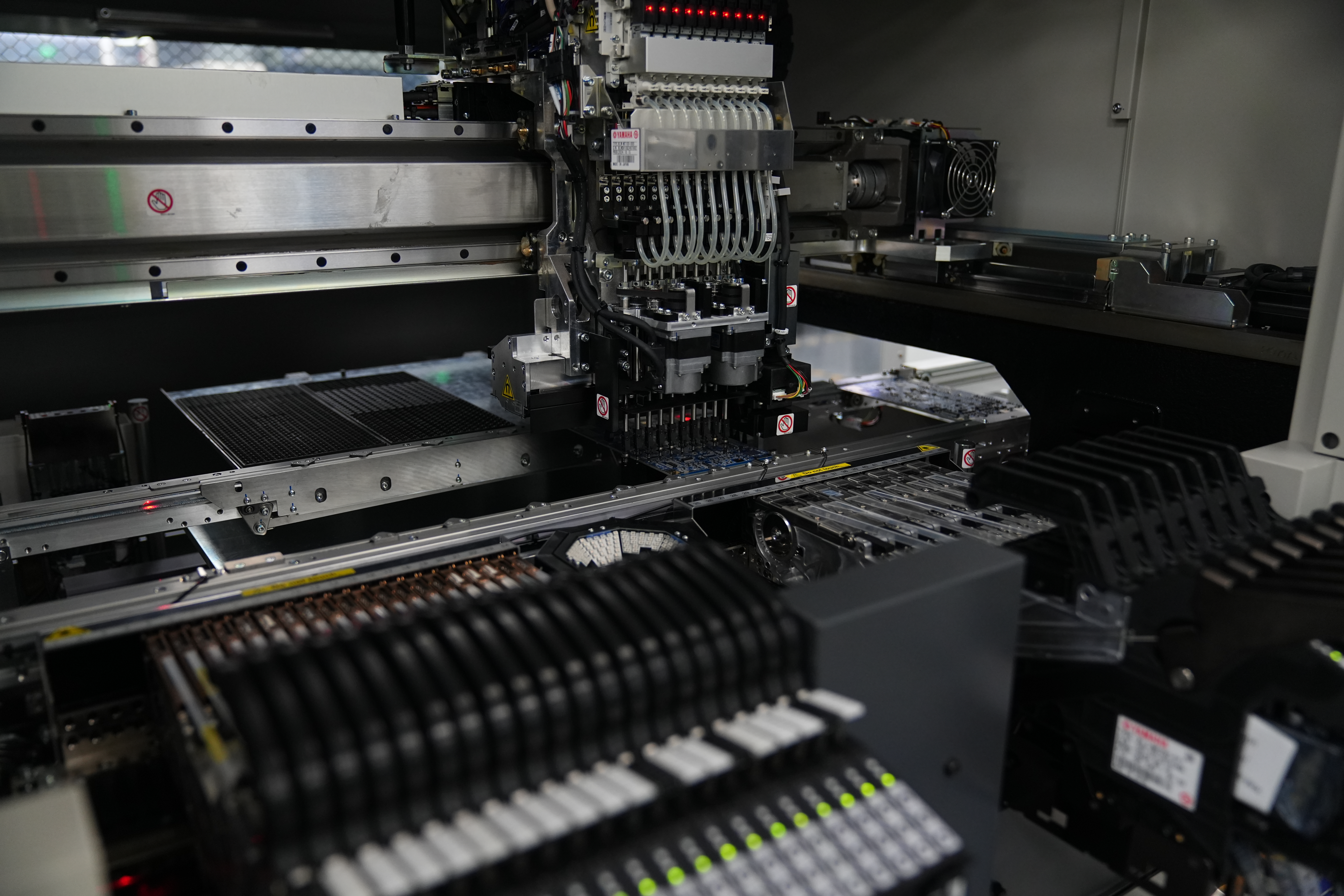
Surface mount technology places components directly onto the board surface. No holes are needed for most parts.
This approach allows higher density. Boards can be smaller and lighter. Most modern printed circuit board assembly manufacturers focus on this method. It suits automation and high-volume production.
Mixed Technology Assembly
Some assemblies combine both methods. Sensitive or heavy parts may use through-hole, while smaller parts use surface mount.
Prototype Printed Circuit Board Assembly
Prototype assembly focuses on early design stages. Volumes are low. Speed matters more than cost. This type supports testing and refinement. Many printed circuit board assembly services specialize in fast prototype builds.
Each type serves a purpose. The best choice depends on product goals, budget, and lifecycle.
How Does a Circuit Card Work?
A circuit card assembly works by guiding electrical signals along designed paths. These paths connect components in a precise sequence.
Power enters through a connector or contact. It flows through regulators and filters. These parts stabilize voltage.
Signals then move into active components. Processors read inputs. Logic circuits decide actions. Outputs leave the board through connectors, displays, or motors. Signal integrity matters. Layout matters.
Even small design choices affect performance. Trace width, spacing, and grounding all play roles. A circuit card does not act alone. It interacts with firmware, mechanical housing, and external systems.
What Does a Circuit Card Assembly Do?
A circuit card assembly acts as the control center of an electronic device. It manages power, data, and interaction.
In some products, it handles simple switching. In others, it runs complex software. Its job is to turn input into output. Buttons become actions. Sensors become data. Signals become results.
A well-built assembly delivers stable performance. It handles heat. It resists vibration. It lasts for years.

What Are Circuit Card Assemblies Used For?
Circuit card assemblies appear almost everywhere. If a device uses electricity, it likely includes one.
- Consumer Electronics: Phones, laptops, and wearables rely on compact assemblies. Surface mount printed circuit assembly manufacturing supports this demand.
- Industrial Equipment: Factories use assemblies for control systems and automation. These environments demand durability.
- Medical Devices: Medical equipment depends on accuracy and safety. Circuit card assemblies control imaging, monitoring, and diagnostics. Quality standards are strict. Traceability matters.
- Automotive Systems: Vehicles contain dozens of assemblies. They manage engines, safety systems, and infotainment. Temperature resistance and long life are critical.
- Communication Systems: Routers, base stations, and networking gear rely on high-speed assemblies. Signal integrity and layout design play major roles.
What Is the Difference Between Circuit Card Assembly and PCB Assembly?
This question comes up often. The terms are closely related, yet they emphasize different stages.
A printed circuit board is the bare board. It has copper traces and holes, but no components.
- A printed circuit board assembly includes components mounted and soldered. It is functional.
- A circuit card assembly usually refers to the same assembled board. The term highlights readiness for use.
In many industries, people use these terms interchangeably. Still, “circuit card assembly” often appears in defense, aerospace, and industrial sectors.
What Are the Applications of Circuit Board Assemblies?
Circuit board assemblies support modern life. Their applications keep expanding as technology evolves.
- They power smart homes.
- They control renewable energy systems.
- They drive automation.
- They support innovation.
As demand grows, so does the need for skilled manufacturers. Printed circuit board assembly manufacturers now offer advanced inspection, testing, and box build options. Box build printed circuit board assembly services go even further. They deliver complete systems, not just boards.
In global markets, China printed circuit board assembly plays a key role. Scale, experience, and supply chain strength support competitive production. With long-term manufacturing experience and a mature supply chain, BEST Technology combines regional strengths with consistent quality control, supporting both high-mix projects and volume production.
Conclusion:
A circuit card assembly is a fully populated and functional electronic board. It combines a printed circuit board with mounted components to create real performance. From consumer electronics to industrial systems, these assemblies power modern life.
For professional printed circuit board assembly services and reliable manufacturing support, contact our team at sales@bestpcbs.com