Many times, when PCB engineer or purchaser seek for a PCB manufacturer to make circuit boards, that always think the price is too high, but don’t know where makes the price is so high and how to optimize the cost on the premise of ensuring the quality of the circuit board. Herein, we share a very useful guideline about “Ten tips to reduce the PCB manufacturing cost”, welcome to read on!

- Substrate
Different brands of substrate have different price. For a simple example, if you require a multi-layer PCB, Tg should greater than 150o, and PP need to over 0.20mm, then use GDM will cheaper than KB or SL. But GDM is usually used for making single or double-sided PCB, it is not recommended to make multi-layer circuit board. If you need to fabricate an 8 layers of multi-layer PCB, KB Tg170 is ideal for your choice since it has good performance and relatively cost-efficient.
- Solder mask oil
In generally, what we should consider about the solder mask (S/M) are color and brand.
For the solder mask color, the most commonly used are green, white and black, if you would like to choose other special colors such as blue, yellow, gray, the price will be a little more costly.
From the brand aspect, currently the best brand is Taiyo solder mask, because it has high viscosity, stable dielectric constant, good insulation and oxidation resistance properties, but it is more expensive than others. Other brands of solder mask oil will be relatively cheap, but the quality is not particularly stable and can’t be guaranteed. So if the circuit boards need to used on bulk products, we recommend to use Taiyo to get a stable quality.
- Printing film
If it is a bulk order with simple design and trace width/space >= 5/5mil, almost manufacturers will use printing film to generate traces. But please remember: the larger the board size, the higher cost of film. (Generally speaking, Prototypes or small orders are use LDI exposure machine to generate the trace, but for mass production, manufacturer will priority choose film and then use LDI.)
- Line width/space
The thinner traces, the higher manufacturing price. Because the line is thinner, the accuracy of the equipment and the quality of the chemical solution are required to be relatively high, and the yield will be relatively low, resulting in higher costs. Each manufacturer has its capability, so choose a suitable supplier is most important, view Best’s website to check our capability.
- Drill holes
The smaller the hole, the higher the price, the diameter of less than 0.3mm will increase the price. The more holes there are, the higher the price will be. Other special holes will also increase the cost, such as half holes, blind holes, PTH holes larger than 6.0mm, etc. Because the hole is small, only one board can be drilled at a time when drilling the hole on PCB material, which is low efficiency and the possibility of drilling a broken drill bitter is also large, resulting in higher cost.
- Finished copper thickness
Finished copper thickness ≥2oz, and hole copper >25μm board will increase the cost. Because the price of copper itself is relatively expensive, the thicker the copper, the higher the price, coupled with the cost of additional electric copper, leads to the overall price rise.
- Finished board thickness
There is little difference in the price of PCB with board thickness of 1.2mm and 1.6mm, but if the board thickness is 2.0mm or even thicker, its cost will increase correspondingly. The thicker the board, the more sheets of fiberglass, so the cost will increase accordingly.
- Outline
If there are more slots, and the slots are less than 1.0mm, the cost will increase. This is because the gong groove of the board is more shaped, resulting in the processing time is elongated. In addition, if the width of the groove is small, processing can not be too fast, easy to break the milling cutter, so the processing efficiency is low, the natural production cost increases.
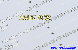
- Surface treatment
Our common surface treatment processes are: OSP(antioxidant), lead HASL, lead-free HASL (environmental protection), gold plating, immersion gold, ENEPIG and some combination processes. The price of the above process is more expensive in turns, that is, OSP (antioxidant) < lead HASL < lead free HASL < gold plating < immersion gold < ENEPIG.
- Tooling fee and testing fee
Tooling fee: in generally most of manufacturers use milling cutter to punch outline if this is a prototype order or small order. But if bulk order, it is needed to use a tooling jig, so there is a tooling fee need to pay.
Testing fee: flying probe tester is usually for small order, mass production need to use testing jig, and there is a different testing fee for both.
Above elements can affect the cost of making a board, you can try to follow those guidelines if you have a limited budget. Or if you want to know a exactly cost, please send RFQ to Best Technology, our sales will give you a best price.