

Gold circuit board designs integrate a thin layer of gold onto specific conductive areas of a PCB, leveraging gold’s exceptional properties to ensure superior signal integrity, reliability, and corrosion resistance in demanding applications. This article provides a comprehensive guide to everything you need to know about gold in PCBs, from its fundamental role and locations to design considerations and how to choose the right manufacturing partner.
Engineers and procurement specialists specifying gold for their PCB designs often face significant challenges in balancing performance with cost and manufacturability. Are you struggling with these common dilemmas?
- Uncertain ROI: The high material cost of gold raises questions about its true necessity and long-term value for a specific application.
- Inconsistent Plating Quality: Varying gold thickness, porosity, or nickel underlayer quality from suppliers leads to unreliable solderability and contact performance.
- Supplier Capability Gaps: Many standard PCB manufacturers lack the specialized expertise for consistent, high-quality gold plating on circuit boards, especially for complex designs.
- Design for Manufacturing (DFM) Hurdles: A lack of clear guidelines for circuit board gold traces and circuit board gold fingers results in suboptimal designs that are difficult or expensive to produce.
- Confusion on Sourcing & Value: Uncertainty about what parts of circuit boards contain gold, what circuit boards have the most gold, and whether it is worth scrapping circuit boards for recovery complicates material and end-of-life decisions.
The solution lies in partnering with a manufacturer that provides not just plating services, but complete engineering support and transparency. Here is how a specialist addresses these core issues:
- Application-Specific Justification: We provide clear analysis on when gold is essential (e.g., for reliable signal transfer in high-frequency or low-voltage applications) versus when alternatives may suffice, ensuring optimal cost-performance.
- Guaranteed Plating Consistency: Our controlled ENIG (Electroless Nickel Immersion Gold) and electroplated hard gold processes ensure uniform thickness, minimal porosity, and a robust nickel barrier, directly solving issues of how to test circuit board for gold quality—we do it for you.
- Specialized Production Expertise: As a factory equipped for advanced finishes, we master the technical challenges of gold circuit board manufacturing, from precise bath chemistry control to automated plating lines.
- Proactive DFM Guidance: Our engineers offer expert gold circuit board design review, specifying optimal gold thickness for traces and fingers, and recommending beveling where needed to prevent wear and ensure smooth mating.
- Full Transparency & Support: We educate clients on where is the gold on a circuit board, its purpose, and even the recoverable value, turning confusion into clear strategic knowledge.
At BEST Technology, we are a specialist in advanced PCB surface finishes, including high-reliability gold plating on circuit boards. We combine rigorous process control with greater technical expertise to deliver boards where the gold layer is not just a cost, but a guaranteed performance enhancer. For your custom gold circuit board needs, pls feel free to contact us at sales@bestpcbs.com.
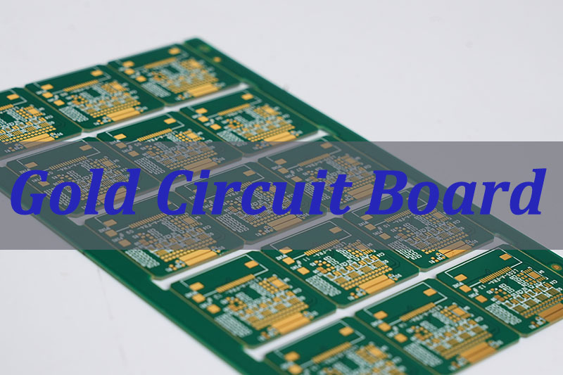
What a Gold Circuit Board Is?
A gold circuit board is not a board made of solid gold, but a standard PCB (typically FR-4) that has critical copper features—such as contact pads, edge connectors (gold fingers), or bonding areas—plated with a thin layer of gold. This gold layer acts as a protective and performance-enhancing coating over a nickel underlayer (in the case of ENIG) or directly over copper (for selective hard gold).
Key Characteristics:
- Construction: A thin gold surface finish (0.05-3.0 µm) applied to specific areas.
- Primary Types:
- ENIG (Electroless Nickel Immersion Gold): The most common. A thin, flat gold layer over nickel, excellent for soldering and wire bonding.
- Electroplated Hard Gold: A thicker, harder gold-cobalt/nickel alloy used on circuit board gold fingers for high-wear applications like card edge connectors.
- Purpose: To provide a non-oxidizing, highly conductive, and reliable surface for electrical contact, soldering, or wire bonding.
Why Is Gold Used in Circuit Boards?
Gold is specified in PCB designs for its unmatched combination of physical and chemical properties, directly enabling strong conductivity and long-term reliability where other metals fail.
- Exceptional Corrosion & Oxidation Resistance: Gold does not oxidize or tarnish in air. This ensures a perfectly reliable, low-resistance contact surface indefinitely, unlike copper or silver.
- Superb Electrical Conductivity: While slightly less conductive than copper or silver, gold’s surface remains pristine, guaranteeing stable, low-contact resistance—critical for low-voltage signals and high-frequency applications.
- Excellent Solderability & Wire Bondability: Gold surfaces wet easily with solder and are ideal for fine gold wire bonding in chip-on-board (COB) and semiconductor packaging, forming reliable interconnections.
- High Durability & Wear Resistance (Hard Gold): Electroplated hard gold withstands the repeated insertion and removal cycles of connectors (gold fingers), preventing wear and maintaining signal integrity.
- Long-Term Shelf Life: PCBs with gold finishes can be stored for years without degradation of their solderability or contact performance.
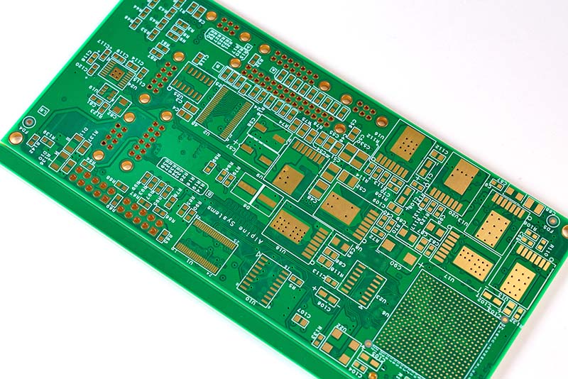
Where Is the Gold on Circuit Boards?
The gold on a PCB is not visible everywhere; it is selectively applied to specific functional areas. Knowing where is the gold on circuit boards helps in design, inspection, and even identifying gold circuit board components for recycling.
| Location | Purpose | Typical Gold Type | Visibility |
|---|---|---|---|
| Edge Connectors (Gold Fingers) | For repeated insertion. | Electroplated Hard Gold (3–50 µ”) | Visible gold tabs on board edge. |
| Surface Mount (SMT) Pads | Supports clean soldering. | ENIG (2–5 µ”) | Matte gold pads on surface. |
| Through-Hole (PTH) & Via Holes | Prevents oxidation. | ENIG | Inside holes; seen up close. |
| Test Points & Probe Contacts | For stable test probing. | ENIG or Selective Hard Gold | Small gold pads. |
| Wire Bonding Pads | For chip wire bonding. | ENIG (tight control) | Near main chip area. |
What Parts of Circuit Boards Contain Gold?
Not all components or boards are created equal in terms of gold content. This is a key consideration for both design and end-of-life recovery. The highest concentrations are found on:
- High-Performance Connectors & Backplanes: Server motherboards, communication backplanes, and high-reliability industrial controls use gold-plated connectors extensively.
- Memory Modules (RAM, DIMMs): The gold fingers on these modules are a classic example of hard gold plating for wear resistance.
- Central Processing Units (CPUs) & Chip Packaging: The substrate and lid of high-end CPUs often have gold plating. The chip die itself may use gold bonding wires and bumps.
- Older & High-Reliability Electronics: Vintage computers, military, aerospace, and medical electronics historically used more gold. Cell phone circuit boards contain some gold, but the amount in modern, miniaturized devices is minuscule.
- Network Switches & Telecom Equipment: Equipment designed for 24/7 operation in data centers frequently uses gold finishes for maximum reliability.
To directly answer a common query: what PC part has the most gold? Historically, the CPU and specialized connector cards held the highest value, but by weight, the concentration on any single modern board is very low (typically less than 0.1 grams per kg of board).
Do All Circuit Boards Contain Gold?
No, not all circuit boards contain gold. The use of gold is a deliberate and costly design choice for specific performance needs.
- Boards WITHOUT Gold: The vast majority of consumer electronics (e.g., TV remotes, basic appliances, low-cost toys) use lower-cost finishes like HASL (Lead-Free Solder), Immersion Silver (ImAg), or OSP (Organic Solderability Preservative). Is there gold in a TV remote? Almost certainly not.
- Boards WITH Gold: Gold is used where its properties are economically justified:
- High Reliability Needs: Medical, automotive, aerospace, and industrial controls.
- Fine-Pitch Components: Where superior solder joint quality is critical.
- Frequent Connection Cycles: Anywhere with connectors that are repeatedly plugged/unplugged.
- Signal Integrity Demands: High-frequency RF and high-speed digital applications.
What Are Circuit Board Gold Traces and Why Do Electronics Use Them?
Circuit board gold traces refer to conductive pathways on the PCB that have been plated with gold, typically via the ENIG process over the underlying copper trace.
- How They’re Made: The entire copper circuitry is coated with a thin layer of nickel and then immersion gold.
- Why Use Them?
- Surface Preservation: Precludes oxidation of the copper, ensuring perfect solderability and bondability even after long storage.
- Flat Surface: Essential for the precise soldering of modern, fine-pitch components like BGAs and QFNs.
- Reliable Connectivity: Guarantees stable contact resistance for test points and exposed circuitry.
- Wire Bonding Compatibility: The gold surface is ideal for creating gold wire bonds directly from semiconductor chips.
How Do Circuit Board Gold Fingers Improve Reliability and Signal Transfer?
Circuit board gold fingers are the gold-plated contacts along the edge of a PCB designed to plug into a matching socket. They are critical for reliable signal transfer.
- Material: Made with “hard gold” (an alloy of gold with cobalt or nickel), which is much more wear-resistant than pure, soft gold.
- Benefits for Reliability & Signal Transfer:
- Low and Stable Contact Resistance: Gold’s oxide-free surface ensures consistent electrical connection, vital for high-speed data buses (e.g., PCIe, RAM interfaces).
- High Durability: Withstands hundreds or thousands of insertion cycles without significant wear or corrosion.
- Corrosion Resistance: Immune to environmental factors that would degrade tin or copper contacts.
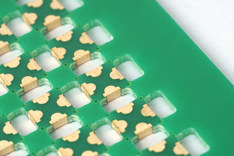
How Does Beveling Improve the Performance of Circuit Board Gold Fingers?
Beveling is the process of machining the leading edge of the circuit board gold fingers into a smooth, angled slope—commonly 30°, 35°, or 45°. This tapered edge guides the gold fingers into the mating connector with minimal friction, preventing harsh impact and mechanical scraping during each insertion.
Primary Purpose
To create a smooth lead-in surface that allows low-force entry into the connector, avoiding damage to both the gold plating and the connector’s internal contacts.
Performance Improvements
1. Prevents Physical Damage
The beveled edge protects the plated hard gold surface from being scraped or chipped, helping maintain low contact resistance and long-term signal stability.
2. Ensures Consistent Mating
The angled entry supports repeatable insertion—important for devices assembled by automated machinery, where connectors must align quickly and reliably.
3. Extends Connector Life
By reducing mating friction, beveling decreases wear on both the gold fingers and the connector socket, extending the cycle life of the entire interconnect system.
Bevel Depth (Chamfer Depth) Explained
In PCB engineering, bevel depth refers to how far the bevel cuts into the PCB thickness. This depth depends on the bevel angle and the board thickness.
Standard Formula
Bevel Depth = Board Thickness × tan(Bevel Angle)
Example Calculations (Based on 1.6 mm PCB Thickness)
At 30° Bevel:
Bevel Depth = 1.6 mm × tan(30°) ≈ 0.92 mm
At 35° Bevel:
Bevel Depth = 1.6 mm × tan(35°) ≈ 1.12 mm
At 45° Bevel:
Bevel Depth = 1.6 mm × tan(45°) = 1.6 mm
Practical Guideline in Manufacturing
Most PCB manufacturers (including EBest Circuit (Best Technology)) follow:
• 30° bevel → smooth entry, minimal cut depth
• 45° bevel → more aggressive slope, used for connectors requiring frequent insertion cycles
• Bevel depth typically kept between 0.8–1.2 mm for 1.6 mm boards unless otherwise specified.
Why Bevel Depth Matters
A proper bevel depth:
• Prevents the connector from catching the PCB edge
• Reduces pressure on plating during mating
• Avoids over-cutting that may expose inner copper layers
• Ensures mechanical alignment in high-cycle applications (e.g., PCIe, edge-card modules)
Why Choosing EBest Circuit (Best Technology) for Gold Circuit Board Production and PCBA Services?
Selecting the right partner for gold circuit board manufacturing is crucial, as the process requires precision and expertise to ensure the gold’s value translates into performance, not waste.
- Guaranteed Process Control: We maintain strict control over our ENIG and hard gold plating baths, ensuring consistent thickness, composition, and minimal porosity—key to answering how to test circuit board for gold quality with efficiency. We always keep in mind that quality is the most important factor in improving our customer retention rate.
- Expert Application Guidance: We help you determine the optimal gold type (ENIG vs. Hard Gold) and thickness for your specific application, preventing over-specification and unnecessary cost.
- Advanced Manufacturing Capability: Our facilities are equipped for high-precision beveling of gold fingers and handling complex designs with mixed surface finishes. All of our PCB fabrication process are fully compatible with ISO 9001, ISO 13485, IATF 16949, AS9100D, UL, REACH, and RoHS.
- Full-Spectrum PCBA Service: We provide turnkey PCB assembly (PCBA), handling the sensitive soldering processes onto gold-plated pads with expertise, preventing issues like gold embrittlement in solder joints. We have PCB and PCBA plants in China. And to meet different needs from different PCB projects, we have set up an SMT factory in Vietnam.
- Transparency & Technical Support: From design review (DFM) to final testing, we provide clear communication and data, demystifying the process and ensuring you get a reliably performing product.
All in all, gold circuit board technology is a strategic engineering choice that provides unmatched surface reliability, solderability, and signal integrity for high-performance and mission-critical electronics. This guide has explored its purpose, application, and the critical design and manufacturing considerations.
For gold circuit board designs that truly deliver on the promise of strong conductivity and long-term reliability, partner with a specialist who masters the art and science of advanced surface finishes. BEST Technology combines rigorous process control with deep technical expertise to ensure your gold-plated PCBs perform flawlessly. Pls feel free to contact us to discuss your project requirements via sales@bestpcbs.com.