

PCB warpage is one of the most common yet misunderstood defects in electronics manufacturing. Whether you are designing, fabricating, or assembling PCBs, understanding pcb warpage meaning, its causes, how to measure it, and how to prevent it is critical to ensuring product quality and assembly reliability. Excessive warpage can lead to component misalignment, soldering defects, mechanical stress, and even field failures.
This guide explains everything you need to know about PCB warpage, including IPC standards, calculation methods, inspection techniques, and practical prevention strategies.

What Is Warpage in PCB?
PCB warpage refers to the maximum vertical deviation of the board surface from an ideal flat plane and is typically expressed as a percentage. The standard calculation formula is:
Warpage (%) = (Maximum warpage height H ÷ Board diagonal length D) × 100%
According to IPC requirements, general-purpose PCBs should have warpage ≤ 0.75%, while carrier boards or backplanes have stricter limits, typically ≤ 0.50% for Class 3 products. During evaluation, it is important to distinguish between bow (cylindrical bending of the board) and twist (three corners lying in one plane while the fourth corner deviates), as this helps identify the underlying cause of deformation.
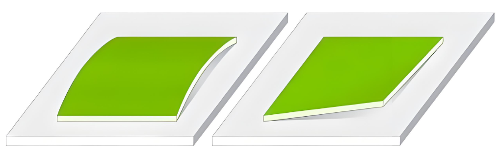
Warpage typically appears in three structural forms:
- Bow – curvature along the length or width
- Twist – diagonal deformation where corners lift unevenly
- Bow + twist – the most common condition in multilayer PCBs
Unlike elastic bending, warpage is often residual, meaning the board does not return to flatness after stress is removed.
What Causes Warpage?
PCB warpage is typically the result of combined effects from material properties, design weaknesses, manufacturing processes, and environmental influences. These factors interact throughout fabrication and assembly, gradually introducing internal stress that exceeds the board’s mechanical stability. Below is a structured engineering explanation of the primary causes.
- CTE mismatch
Copper has a coefficient of thermal expansion (CTE) of approximately 17 ppm/°C, while FR-4 resin systems typically range from 50 to 70 ppm/°C. During heating and cooling cycles, these materials expand and contract at different rates, generating internal stress that leads to bending or twisting.
- Moisture absorption
Resin-based laminates absorb moisture during storage. When exposed to high temperatures during reflow soldering, absorbed moisture rapidly vaporizes. This phenomenon, often described as the “popcorn effect,” creates localized internal pressure that can cause deformation or permanent warpage.
- Asymmetrical copper distribution
When one side of the PCB contains large copper planes (such as solid ground layers) and the opposite side has sparse routing, thermal contraction during cooling becomes uneven.
- Unbalanced layer stack-up
In multilayer boards, asymmetry in core thickness, prepreg count, or material type above and below the neutral axis leads to uneven stress during lamination. For example, a 6 layer PCB with thicker inner layers on one side will deform more easily during heating and cooling.
- Lamination issues
Rapid heating rates (greater than 3 °C per minute), uneven pressure distribution, or insufficient curing time during lamination can leave residual stress trapped inside the PCB after press release.
- Soldering thermal impact
Excessive reflow temperatures (above 260 °C) or overly aggressive cooling rates (greater than 4 °C per second) intensify CTE mismatch effects. This is particularly critical for lead-free assembly processes.
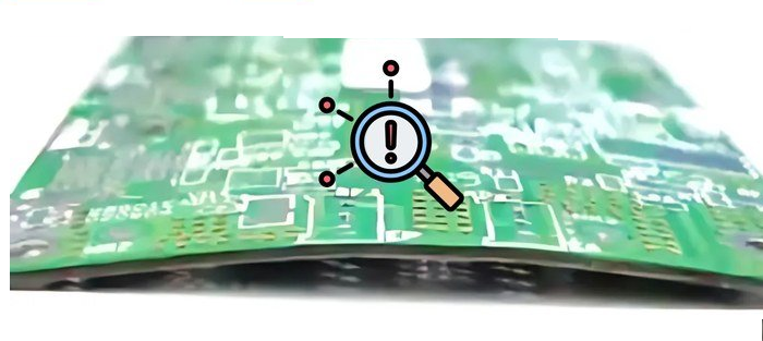
What Are the Signs of Warpage?
Warpage often manifests indirectly during fabrication or assembly.
Typical indicators include:
- Board does not sit flat on a surface
- Corners lifting off the table
- Twisting along diagonal axis
- Poor solder joints on one side
- Open or short circuits after assembly
- BGA or QFN soldering failures
- Difficulty during pick-and-place
In high-volume SMT lines, elevated defect rates are often the first signal that warpage exceeds process tolerance.
Is Warpage Considered a Defect?
Yes – excessive warpage is considered a defect.
However, small amounts of warpage are allowed within IPC standards. If warpage exceeds specified limits, the PCB is considered non-conforming and may be rejected.
Whether warpage is a defect depends on:
- IPC class (Class 1, 2, or 3)
- End application (consumer, industrial, medical, aerospace)
- Assembly process tolerance
This is why pcb warpage meaning must always be interpreted in the context of measured values versus acceptance criteria.
PCB Warpage in IPC Standard Datasheet
PCB warpage limits vary by industry, application, and assembly condition. International standards and sector-specific requirements define acceptable warpage ranges to ensure assembly reliability and mechanical integrity. The most commonly referenced standards are outlined below.
In IPC-A-600G, For bare rigid PCBs, the maximum allowable warpage is typically 1.5%. For assembled PCBs with components mounted, the allowable warpage is more stringent, generally limited to 0.75% to ensure SMT process stability. However, HDI (High Density Interconnect) boards usually require warpage to be controlled within 1.0%, and in many cases even lower depending on customer specifications.
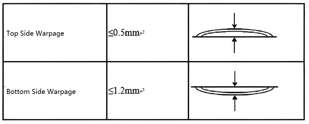
Here is a detailed table show the PCB warpage standards for each kind of PCB:
| PCB Application | Maximum Allowable Warpage |
| SMT assemblies | ≤ 0.75% |
| Through-hole boards | ≤ 1.5% |
| Fine-pitch / BGA designs | ≤ 0.5% (often tighter by OEM) |
| HDI PCB | ≤ 1.0% |
Many automotive, medical, and aerospace programs impose stricter internal limits, sometimes as low as 0.3%, to ensure solder joint reliability.
PCB Warpage Calculation
The standard pcb warpage calculation formula is:
Warpage (%) = (Maximum deviation ÷ Board length or diagonal) × 100
Example:
Board length = 250 mm
Maximum deviation = 1.25 mm
Warpage = (1.25 ÷ 250) × 100 = 0.5%
This calculation method is consistent with IPC acceptance practices and customer audit requirements.
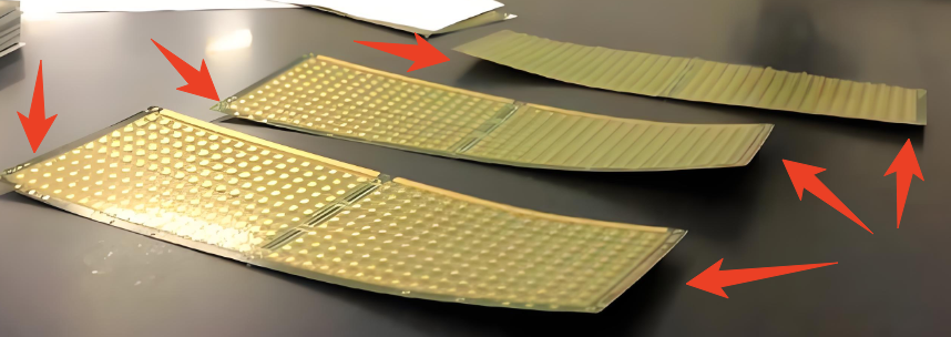
How to Check PCB Warpage?
Inspecting printed circuit board (PCB) warpage requires standardized methods, appropriate measurement equipment, and controlled procedures to ensure accuracy and repeatability. Several inspection methods are widely used, depending on accuracy requirements and production volume:
- Feeler Gauge Method
Suitable for quick sampling inspections on production lines. The PCB is placed horizontally on a flat platform, and a feeler gauge is inserted into the largest gap between the board and the surface to obtain height H. This method is simple but has limited accuracy and is often used alongside optical methods for confirmation.
- Optical Projector / Vision Measurement Method
The PCB outline is projected optically, and the height difference (ΔH) between the reference plane and the lifted corner is measured. This method offers high accuracy, up to 0.001 mm, and requires the board to stabilize for at least 4 hours under standard conditions (temperature 23 ± 3 °C, humidity 50% ± 10%).
- Laser Scanning Method
A matrix of laser displacement sensors scans the PCB surface to generate a 3D topography map. Software automatically calculates warpage values with typical accuracy of ±0.01 mm, making this method suitable for HDI boards and automated inspection lines.
- Non-Contact Optical Scanners
Advanced systems based on phase-measuring deflectometry (PMD) can rapidly capture full-board 3D data without surface contact, eliminating the risk of mechanical damage. High-end models also support dynamic warpage measurement at elevated temperatures.
How to Prevent PCB Warpage?
Prevention begins at the design stage and continues through fabrication and assembly.
Design-Level Prevention
- Use symmetrical stack-ups
- Balance copper distribution on all layers
- Avoid large, unbroken copper areas
Material Selection
- Choose laminates with stable thermal behavior
- Match prepreg and core thickness carefully
- Avoid unnecessary mixed material systems
Fabrication Controls
- Controlled lamination temperature ramps
- Uniform cooling after press cycles
- Stress-relief baking where appropriate
Assembly Controls
- Use proper pallet support during reflow
- Minimize unnecessary thermal cycles
- Control reflow profiles tightly
When these measures are combined, warpage risk drops significantly.
How Do You Fix a Warped PCB?
Once warpage occurs, options become limited. Correction is possible, but it is not always permanent.
Common Remediation Methods
- Controlled thermal flattening under pressure
- Fixtured re-baking processes
- Mechanical straightening for low-risk products
Practical Limitations
- Reworked boards may re-warp during operation
- Mechanical stress can reduce long-term reliability
- Not suitable for high-reliability applications
In most cases, prevention is far more effective than correction.
Why Choose Best Technology (EBest Circuit) as Your PCB Manufacturer?
Controlling PCB warpage is not only a design challenge; it is a manufacturing discipline. This is where Best Technology differentiates itself as a reliable PCB manufacturing partner for global customers.
Best Technology (EBest Circuit) has extensive experience producing multilayer PCBs, HDI boards, thick copper PCBs, metal core PCBs, and rigid-flex boards, all of which are naturally more susceptible to warpage if process control is weak. Our engineering team evaluates warpage risk at the quotation and DFM stage, not after defects appear.
We are certificated with ISO9001/13485, AS9100D, IATF16949, all of our PCB and PCBA products are strictly follow IPC class II and III. In additional to this, our facility has introduced MES system, this ensures the full traceability of all products.
If you are looking for a PCB manufacturer that truly understands pcb warpage meaning, prevention, and real-world assembly requirements, our engineering team is ready to support your next project.
FAQs
1. What is the acceptable PCB warpage limit?
Most standards allow ≤0.75%, while high-reliability boards typically require ≤0.50%.
2. Can PCB warpage affect BGA solder joints?
Yes. Even slight warpage can cause non-uniform solder collapse and early joint failure.
3. Does PCB thickness reduce warpage?
Thicker boards are generally more resistant, but thickness alone does not solve imbalance issues.
4. Is warpage more common in multilayer PCBs?
Yes. As layer count increases, stress imbalance becomes harder to control.
5. Can reflow soldering cause warpage?
Multiple reflow cycles and improper support frequently increase warpage risk.