

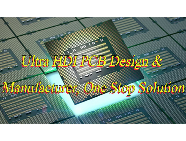
What is ultra HDI PCB? This blog cover technical parameter, typical applications, design consideration, production process and cost for ultra HDI PCB board.
Are you troubled with these problems?
- Are your ultra-high-frequency signals suffering from increased signal loss and crosstalk issues under micro-line widths?
- Repeated revisions of multi-stage HDI designs driving up both time and cost – how to break the cycle?
- Struggling with slow responses and yield fluctuations for small-batch, multi-variety orders from traditional HDI suppliers?
As a ultra HDI PCB manufacturer, EBest Circuit (Best Technology) can provide you service and solution:
- Design-Simulation-Manufacturing end-to-end rapid response service slashes product launch cycles by 30% with 48-hour design iteration validation!
- Leveraging LDI + electroplating via-filling technology to achieve 25μm line width/spacing precision – ensuring signal integrity even under high-frequency demands!
- Customizable mass production solutions for small-batch, multi-variety orders – 72-hour rapid delivery to flexibly support high-frequency iteration needs in consumer electronics and 5G devices!
Welcome to contact us if you have any request for ultra HDI PCB board: sales@bestpcbs.com.
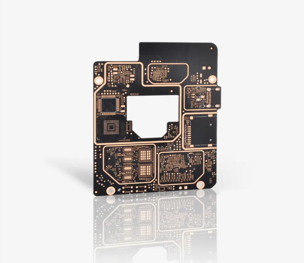
What Is Ultra HDI PCB?
Ultra HDI PCB represents the pinnacle of PCB manufacturing technology, characterized by extreme wiring density and interconnection complexity far exceeding conventional HDI boards. It achieves this through ultra-fine line width/spacing (typically ≤50μm, down to 30μm or smaller), micro-laser drilling (≤50μm microvias/blind vias), advanced any-layer interconnection or stacked microvia structures, and processes like via-in-pad plating.
Production requires top-tier materials (e.g., ultra-low loss substrates), precision equipment (e.g., ultra-fine laser drills), and rigorous process control. Its core value lies in providing essential signal integrity, power density, and ultra-miniaturization solutions for cutting-edge applications including 5G/6G communication, advanced AI servers, high-performance computing (HPC), miniaturized wearable/medical devices, and space-constrained aerospace electronics.
Ultra HDI PCB Technical Parameter
| Parameter Category | Technical Specifications |
| Layer Configuration | 4-20 layers |
| Thickness Range | 0.3mm–2.0mm |
| Line Width/Spacing | 30μm/30μm (minimum) |
| Microvia Technology | Diameter: 0.07–0.13mm (typical 0.10–0.40mm) |
| Aspect ratio | 1:1 |
| Materials | FR-4 high Tg, halogen-free, Rogers high-frequency |
| Surface Finishes | ENIG, OSP, immersion tin/silver |
| Impedance Control | ±5% tolerance (100Ω differential/50Ω single-ended) |
| Stack-up & Lamination | Any-layer HDI, sequential lamination |
| Laser Drilling | ≤50μm precision |
| Registration Accuracy | ±25μm |
Typical Applications of Ultra HDI PCB Board
- Smartphones and Tablets: Motherboards, camera modules, RF modules, etc., with flagship models prioritizing thinner designs and more powerful capabilities.
- Wearable Devices: Smartwatches, health monitoring devices, etc., facing extreme space constraints.
- High-End Laptops and Ultrabooks: Demand for lightweight and compact designs.
- Servers and Data Centers: High-speed computing cards, high-speed interconnection boards and carrier boards in switches and routers, requiring high-density routing to support high-speed signals (e.g., 56Gbps+ SerDes).
- Network Communication Equipment: Core boards for high-end routers, switches, and optical modules.
- Medical Electronics: Implantable devices, endoscopes, portable diagnostic instruments, etc., requiring miniaturization and high reliability.
- Aerospace and Defense Electronics: Radar systems, satellite communications, missile guidance, etc., needing high performance, high density, lightweight design, and high reliability.
- Automotive Electronics (High-End/ADAS/EV): Core control units in advanced driver assistance systems, infotainment systems, and battery management systems.
- IC Substrates: Critical interposer boards connecting dies to conventional PCBs, particularly serving advanced packaging technologies such as FCBGA, SiP, and 2.5D/3D IC.
Ultra HDI PCB Board Design Considerations
Below are considerations for ultra HDI PCB design:
1. Design Rules and Standards Enhanced Implementation
- IPC-2226 Level C+ Standard Precise Implementation: Conductor width strictly controlled at ≤50μm (tolerance ±5μm), isolation spacing ≤50μm (both intra-layer and inter-layer requirements), dielectric thickness ≤50μm with uniformity error ≤3%. 532nm ultraviolet laser drilling technology achieves microvia diameter ≤75μm (aperture tolerance ±2μm), combined with electroplating hole filling process to ensure hole wall copper thickness ≥15μm. 100% defect screening is achieved through AOI inspection system for consistency verification.
- Reliability Accelerated Verification System: Dual validation via 2000 cycles of -55°C to 150°C thermal shock and 1000 hours of 85°C/85%RH humid aging ensures no cracks in microvia filling areas and copper surface flatness error ≤2μm. CTE matching verification uses TMA thermal mechanical analyzer to ensure thermal expansion coefficient difference between copper foil and dielectric layer ≤3ppm/℃, avoiding delamination risks.
2. Stack-Up Structure and Material Selection Strategy
- Hybrid Stack-Up 3D Design: Core layer utilizes high-speed materials (e.g. Panasonic M7) with thickness 100-300μm; build-up layers adopt low-loss resin + ceramic filler system with thickness ≤50μm. ANSYS HFSS simulation optimizes interlayer dielectric thickness gradient to ensure Z-axis CTE decreases from inner to outer layers, reducing thermal stress concentration.
- High-Frequency Material Quantification: M7/M8 grade copper-clad laminates maintain Dk stability at 3.6±0.05 (1-10GHz range) with Df ≤0.004. HVLP (very low profile copper foil) ensures thickness uniformity error ≤5% and signal transmission loss ≤0.5dB/cm@10GHz.
3. Microvia Design and Layout Specifications
- Microvia Filling Process Control: Pulse electroplating achieves 100% microvia filling rate with surface flatness error ≤2μm, supporting Via-in-Pad+Plated Over (POV) design. Laser positioning system ensures microvia grid offset precision ≤15μm, preventing copper residue at pad edges causing short circuits.
- Blind/Buried Via Topology Optimization: Ground via arrays (spacing ≤100μm) are added at signal layer transitions to form low-impedance short loops. 2-stage blind vias replace 3-stage through-holes, reducing lamination cycles and increasing routing density by over 25%. Blind via bottom filling uses conductive adhesive + thermal curing process to ensure contact resistance ≤5mΩ.
4. Signal Integrity Control Measures
- Impedance Matching 3D Calculation: 2.5D/3D impedance simulation via SIwave software ensures trace width ≥3mil (76.2μm) with width tolerance ≤±0.5mil, dielectric thickness error ≤±2%, and copper thickness error ≤±10%. Differential pair impedance is controlled at 100±5Ω, single-ended line at 50±2Ω, with target deviation ≤±3Ω.
- Equal-Length Routing and Termination Strategies: High-speed signals use serpentine routing for length error ≤±5mil, combined with Thevenin termination resistors (e.g. 50Ω series + parallel network) to suppress signal reflection. Signal layers are sandwiched between two ground planes with layer spacing ≤80μm, reducing crosstalk to below -50dB and ensuring eye diagram opening ≥80%.
5. Power Integrity and Thermal Management Solutions
- Power Path Refinement Design: Power pins utilize nearby vias (aperture ≥0.25mm) and trace width ≥25mil (635μm) to reduce inductance to ≤1nH/cm. Decoupling capacitors in 0402 package are placed adjacent to power pins (spacing ≤5mm) with capacity error ≤3%, ensuring power noise ≤50mVpp.
- Thermal Management Integrated System: Heat dissipation via arrays (aperture 0.4mm, spacing 1.5mm) combined with thermal conductivity ≥3W/mK silicone grease ensures power device temperature rise ≤25°C. Low-impedance paths (impedance ≤0.5mΩ) between power and ground layers, paired with EMI filter capacitors, enhance EMC performance to CISPR 22 Class B standard.
6. Component Layout and Density Optimization Methods
- High-Density Component Layout Strategy: BGA pin pitch ≥0.4mm with trace width ≥3mil, using “dog bone” routing to reduce signal delay. Component-to-board edge distance ≥λ/8 (λ is signal wavelength) ensures electrical safety clearance. 0201 package components use “island” pad design to minimize soldering defects.
- PWB Density Quantitative Evaluation: Routing capacity is assessed via average trace length per square inch (≥5000mil/in²), with microvia grid technology (grid spacing ≤150μm) increasing routing density by over 35%. Critical signal areas feature density grading zones with 15% redundancy for later adjustments.
7. Manufacturing and Reliability Assurance System
- Process Capability Collaborative Verification: Joint validation with PCB manufacturers confirms LDI imaging system resolution (≥5μm) and AOI inspection system defect capture rate (≥99.9%). Back-drilling technology reduces stub length to ≤2mil, minimizing signal reflection.
- Test Point Intelligent Planning: Reserved X-ray inspection points (aperture ≥0.35mm) and electrical test points (spacing ≥0.6mm) support 100% in-line electrical testing and offline X-ray inspection. Test points use “cross” design for stable contact.
8. Cost and Performance Balancing Strategy
- Material Grading Selection Scheme: Critical signal layers use M7/M8 grade substrates (20% cost increase), while non-critical layers adopt FR-4 materials (35% cost reduction). Modular design (e.g. separate power modules) reduces process complexity, avoiding excessive cost escalation.
- Process Optimization Pathways: 2-stage blind vias replace 3-stage through-holes, reducing lamination cycles and manufacturing costs by over 18%. Non-critical areas relax impedance tolerance to ±10% for performance-cost balance. Critical zones implement “localized high-density” design, while non-critical areas use “global low-density” layout.
How to Make Ultra HDI PCB Boards?
1. Material Selection and Precise Parameter Setting
- Core board uses ultra-thin low-roughness specialized copper-clad laminate with thickness strictly controlled within 50-100μm range. Surface roughness ≤0.5μm, achieved through nanoscale polishing to ensure copper surface flatness, providing an ultra-high-definition base for subsequent LDI exposure.
- Prepreg (PP) selects high-performance materials with Tg ≥180℃ and CTE ≤20ppm/℃. Thickness tolerance is compressed to ±10%. Vacuum hot-pressing process eliminates interlayer bubbles, ensuring balanced thermal stress distribution in multilayer structures.
- Ultra-thin copper foil (≤12μm) undergoes plasma surface activation treatment, increasing bonding energy to ≥450mJ/m², effectively solving interfacial delamination issues during lamination.
2. Inner Layer Pattern Micron-Level Forming Process
- Dry film coating employs roller-type coater with thickness uniformity controlled at 15-25μm ±2μm. 355nm wavelength LDI laser achieves 5μm resolution exposure. Line width/spacing precision reaches 25μm/25μm with edge burr ≤0.1μm.
- Developing process uses dual-channel spray system with 0.5-1.0% sodium carbonate solution at 28-32℃. Developing time is precisely controlled to ±3 seconds. AI vision detection system dynamically adjusts developing gradient. Etching employs copper chloride-hydrochloric acid system with flow control achieving lateral etching ≤1μm. AOI detection with AI algorithm identifies 0.3μm level circuit defects.
3. Laser Microvia Drilling and Hole Wall Forming
- UV laser drilling machine equipped with high-precision galvanometer scanning system. Pulse energy density stable at 1-10J/cm². Processes blind/buried holes with diameters 50-100μm. Hole position accuracy ±2μm with circularity ≥95%.
- Hole wall quality verified by confocal microscope requires no molten residue or resin remnants, surface roughness Ra ≤0.2μm. For ELIC structures, dual-sided synchronous drilling with vacuum adsorption platform ensures board deformation ≤10μm.
4. Drilling Contamination Removal and Hole Wall Reinforcement
- Chemical desmearing uses potassium permanganate-sulfuric acid solution system at 30-50g/L concentration and 50-60℃ temperature for 3-5 minutes. Ultrasonic oscillation enhances cleaning efficiency. Post-treatment hole wall cleanliness meets ASTM D523 standard.
- Etchback process controls etching depth at 1-2μm via alkaline etchant, forming honeycomb micro-rough structure that increases surface area by >30%. Combined with pre-chemical copper activation treatment, copper plating adhesion improves to Grade 5B per ASTM D3359.
5. Hole Wall Metallization and 3D Filling Process
- Chemical copper plating uses formaldehyde-copper sulfate system at 25-30℃ and pH 11.5-12.5. Online conductivity monitoring ensures stable deposition rate of 0.1-0.2μm/min. Thickness uniformity ≤5%, hole wall coverage ≥99.8%.
- Electroplating filling employs pulse plating with forward current density 2-4A/dm² and reverse current density 0.1-0.3A/dm². Proprietary additives achieve complete microvia filling with void ratio ≤1%, density ≥99.5%, surface flatness ±2μm, meeting IPC-6012 standard.
6. Outer Layer Build-Up Pattern Precision Control
- Outer layer dry film uses high-resolution photosensitive material with 20-30μm thickness. LDI exposure achieves 20μm/20μm line width/spacing pattern transfer. Pattern plating copper thickness 20-30μm with uniformity ≤3%.
- Tin plating layer thickness 3-5μm serves as etching mask. Nitric-sulfuric acid system removes tin at 0.5-1μm/min rate, ensuring complete tin removal without damaging underlying copper traces. AOI detection with multispectral imaging system inspects 12 parameters including line width, spacing, and notches with 1.5μm precision.
7. Multilayer Structure Lamination and Alignment Control
- Lamination employs vacuum hot press with precise temperature curve control: preheat 120℃/30min, main press 190℃/90min, cooling rate ≤3℃/min, pressure gradient 50-300psi.
- Optical alignment system uses infrared and visible dual-mode positioning with interlayer alignment accuracy ≤25μm. Stress relief slot design ensures 2+N+2 structure post-lamination warpage ≤0.5%. Real-time monitoring of PP melt flow index ensures interlayer bonding strength ≥150N/cm.
8. Surface Treatment and Precision Outline Processing
- Surface treatment adopts ENIG process. Chemical nickel layer thickness 5-7μm with phosphorus content 8-10%. Gold layer thickness 0.05-0.1μm. Solderability meets J-STD-002 standard, passing 85℃/85%RH/168h high-temperature-humidity test without black pad phenomenon.
- Outline processing uses 5-axis CNC milling machine with diamond-coated tools. Cutting accuracy ±25μm, edge burr ≤5μm. Laser cutting enables micro-slot processing with slot width tolerance ±10μm. Final packaging uses vacuum moisture barrier bags with humidity indicator cards, ensuring transport humidity ≤5%RH.
9. Full-Process Quality Traceability and Verification
- Online AOI detection equipped with deep learning algorithms identifies defects such as shorts, opens, and uneven etching with 1.5μm precision and false call rate ≤0.1%. Electrical testing uses 100MHz flying probe system capable of detecting 5nS signal delays with 100% test coverage.
- Final verification includes microsection analysis with 5% sampling rate. Metallographic microscope verifies hole copper thickness ≥15μm and fill void ratio ≤2%. HALT/HASS testing validates product reliability, ensuring electrical performance degradation ≤5% after 1000 temperature cycles from -40℃ to 125℃, meeting long-term use requirements for high-end electronic devices.
How Much Does Ultra HDI PCB Cost?
| Product Type/Specification | Price Range (USD/㎡) |
| Basic type (4-8 layers) | $41–$110 |
| Advanced type (10+ layers) | $137–$685+ |
| High-end type (AI server grade) | $4,110–$6,850+ |
| Special material (high-frequency) | $116–$137 |
| Bulk pricing (>10㎡ order) | $27–$41 |
Why Choose EBest Circuit (Best Technology) as Ultra HDI PCB Manufacturer?
Reasons why choose us as ultra HDI PCB manufacturer:
- 19 Years of Industry Expertise with Over 10,000 Successful Project Cases: With 19 years of dedicated experience in ultra HDI PCB manufacturing, we have successfully delivered over 10,000 complex projects across 5G base stations, medical imaging equipment, consumer electronics, and aerospace applications. Our deep technical knowledge minimizes trial-and-error costs, ensuring optimal solutions from the start.
- End-to-End One-Stop Service for Cost and Time Efficiency: From design consultation, DFM optimization, and rapid prototyping to volume production, testing, and logistics, our integrated service chain eliminates the need for multiple vendor coordination. This reduces communication costs by 30% and accelerates time-to-market for your products.
- Complimentary Professional DFM Analysis to Mitigate Risks Early: Our free Design for Manufacturability (DFM) analysis identifies potential design flaws, such as line width/spacing issues, layer alignment errors, or impedance mismatches before production begins. This proactive approach saves over 50% of design iteration costs and prevents rework delays.
- 48-Hour Rapid Prototyping with Flexible Small-Batch Customization: We support 24-hour prototyping and 48-hour delivery for small-batch orders starting from just 5 pieces. This flexibility caters to startups, R&D teams, and low-volume high-mix production needs, reducing inventory pressure and capital tie-up.
- Transparent Pricing with No Hidden Costs: Our pricing model is based on layer count, material selection, and process complexity, ensuring clear and fair quotes. Volume orders qualify for tiered discounts, delivering industry-leading cost-performance without surprise fees.
- Robust Quality Control with Full Traceability: Certified under ISO 9001, ISO 14001, and IATF 16949, our 18-step quality control process includes AOI inspection, X-ray layer alignment checks, and flying probe testing. This ensures full traceability from raw materials to finished products, achieving a 99.8% yield rate.
- Precision Equipment for Micron-Level Process Accuracy: Equipped with global-leading LDI laser imaging systems, high-precision drilling machines, and plasma cleaning lines, we enable ultra-fine line/space (≤30μm), blind/buried vias, and any-layer interconnection to meet the highest density and reliability demands.
- Eco-Friendly Manufacturing Aligned with Global Standards: Our processes use lead-free techniques, water-based solder masks, and comply with RoHS, REACH, and ISO 14001 standards. This ensures products meet international environmental regulations, facilitating seamless global market entry.
Choosing EBest Circuit (Best Technology) means prioritizing experience, efficiency, quality, and value. We are committed to being your most reliable partner in ultra HDI PCB solutions. Welcome to contact us via email: sales@bestpcbs.com.