

What is Thermoelectric Separation Copper Based PCB?
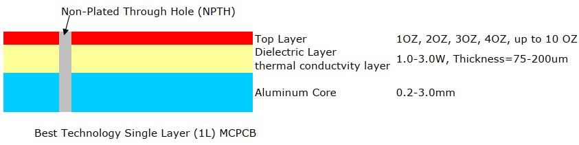
A thermoelectric separation copper based PCB is a special type of metal core PCB that uses thermoelectric separation technology to isolate heat and electrical pathways. Unlike traditional PCBs, this board is designed to separate heat flow from current flow, ensuring that the electronic circuit remains cooler even when high currents are running through it.
The board uses a thick copper layer to handle high current and a ceramic dielectric or polymer insulation to manage thermal conduction. This separation reduces thermal stress on components, improves reliability, and supports better performance in demanding applications such as power electronics, LED systems, and automotive electronics.
How to Distinguish Normal Copper Core PCB and Thermoelectric Separation Copper Based PCB?
1. Definition & Structure
- Regular Copper-Based PCB:
This type includes a metal base, insulating layer, and circuit layer. The copper foil is usually 35μm to 280μm thick to handle high current. The insulating layer is made of alumina, silicon powder, and epoxy resin, offering good thermal resistance and elasticity.
- Thermoelectric Separation Copper-Based PCB:
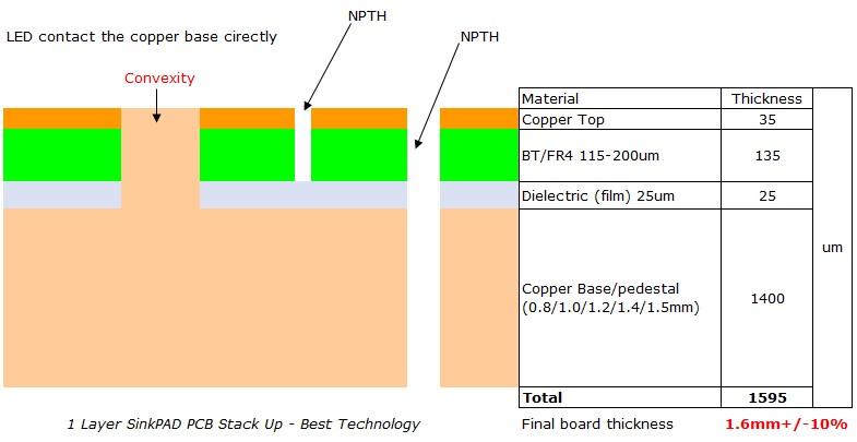
Uses a special process that separates the heat conduction layer from the electrical circuit layer. A copper convexity pad (heat-conductive bump) directly contacts the heat source, providing a direct heat path (zero thermal resistance). Typical structure: Circuit Layer – Convexity Pad – Insulation – Metal Base.
2. Performance Differences
- Thermal Conductivity:
Regular boards rely on insulation materials (1-3W/m·K), limiting heat transfer. Thermoelectric separation boards use copper convexity (up to 400W/m·K), reducing thermal resistance by over 80% and suiting high-power applications (50–500W+).
- Thermal Expansion:
Regular boards expand more with temperature, causing deformation. Thermoelectric boards have a lower coefficient of expansion.
- Dimensional Stability:
Thermoelectric separation boards resist size changes better under temperature shifts, improving assembly precision.
- Mechanical Strength:
Reinforced materials in thermoelectric boards provide higher strength against mechanical stress.
- Electrical Properties:
Thermoelectric boards offer more stable conductivity with fewer defects like uneven resistance or noise.
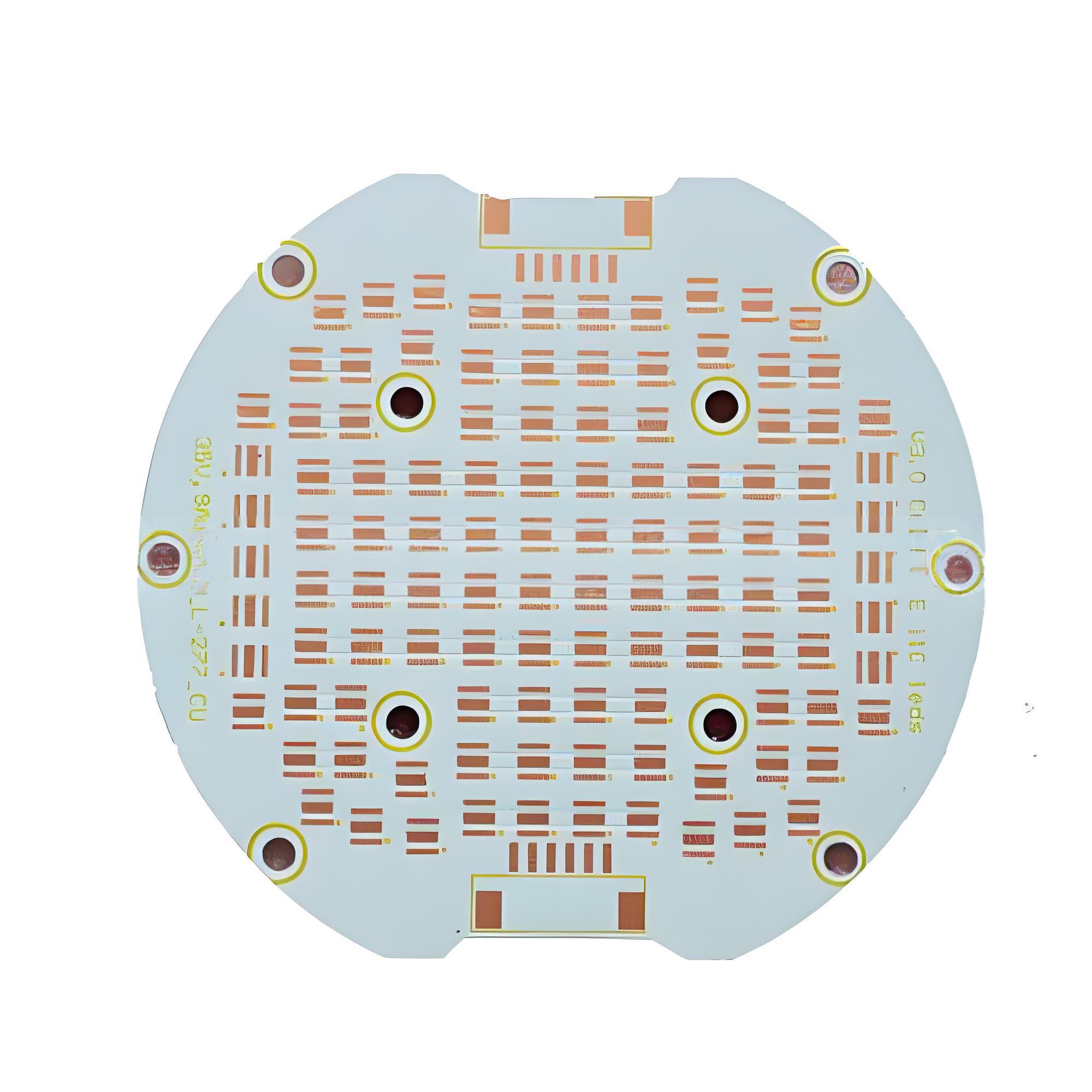
3. Appearance
- Regular PCB: Flat, layered, with no distinct structural features.
- Thermoelectric PCB: Includes visible heat-conductive convexities (usually square or polygonal) to directly touch heat sources.
4. Applications
Regular Copper PCBs:
- Ideal for low-power, general applications:
- Indoor lighting (e.g., ceiling lights, desk lamps)
- Automotive interior electronics
- Small consumer devices (e.g., chargers, smartwatches)
Thermoelectric Separation PCBs:
- Suited for high-power, high-heat devices:
- High-power LED lighting (e.g., automotive headlights, industrial lamps)
- Critical automotive electronics (e.g., engine control, motor drivers)
- High-end electronics (e.g., LED smart TVs needing high-efficiency heat dissipation)
5. Cost & Manufacturing Complexity
- Regular Copper PCBs:
Simple and cost-effective. Follows standard PCB processes: cutting, drilling, imaging, etching, solder mask, surface finish, testing, and packaging.
- Thermoelectric Separation PCBs:
More complex and expensive. Requires additional steps like laser window opening, copper convexity plating, and precise insulation layering, demanding higher technical capability and manufacturing control.
Features of Thermoelectric Separation Technology
Thermoelectric separation technology brings unique benefits to metal core PCBs:
- Independent Heat and Current Paths: It separates thermal conduction from electrical conduction, improving overall system stability.
- Lower Thermal Resistance: Enhances the heat dissipation rate, extending the life of components.
- Thicker Copper Layers: Supports high-current loads without overheating.
- Stable Performance Under High Load: Useful in environments that generate intense heat.
- Improved Reliability: Reduces risks of component failure due to overheating.
This advanced technology is especially important in industries where temperature sensitivity and power delivery go hand in hand, such as inverters, electric vehicles, and industrial power control systems.
Parameters of Thermoelectric Separation Metal PCB
Here are some common technical parameters for thermoelectric separation copper based PCBs:
| Parameter | Value / Range |
| Copper Thickness | 1oz to 12oz (35μm to 420μm) |
| Dielectric Material | Ceramic/polymer insulation |
| Dielectric Thickness | 50μm – 200μm |
| Thermal Conductivity | 2 – 10 W/m·K |
| Thermal Resistance | < 0.3 °C/W |
| Operating Temperature | -40°C to +150°C or more |
| Breakdown Voltage | > 2KV (depending on insulation material) |
| Surface Finish | ENIG, OSP, HASL, etc. |
| Layer Count | 1L to 4L (usually single-layer for high power) |
These parameters can be customized depending on the final application and power demands.
How to Make Thermoelectric Separation Copper Based PCB?
The manufacturing process of a thermoelectric separation copper based PCB is more complex than that of traditional metal core PCBs due to the need to incorporate a convexity pad structure that enables direct heat transfer. This approach demands high precision in material selection, layering, and processing. Below is a detailed overview of how these specialized PCBs are made:
1. Material Selection
The process begins by selecting the appropriate materials:
- Copper Base Plate: A thick copper base (typically 1.0mm–3.0mm or more) is chosen for its excellent thermal conductivity.
- Insulating Layer: A thin dielectric layer is applied, usually a high-performance ceramic or polymer with high breakdown voltage and thermal conductivity.
- Copper Foil: A thick copper foil (ranging from 1oz to 12oz) is used for the circuit layer to support high current loads.
The materials must withstand high thermal stress and provide excellent heat conduction while ensuring electrical insulation between the circuit and the base.
2. Convexity Pad Design and Machining
The most important step in the thermoelectric separation structure is the machining of convex pads (also known as raised thermal columns):
- These convex pads are precisely etched or milled from the copper base or applied using a punching or stamping technique.
- The pads are aligned directly underneath heat-generating components, such as power transistors or LED chips.
- Once mounted, these pads come into direct contact with the component’s thermal pad, allowing the heat to transfer directly to the copper base, bypassing the insulating layer.
This is what separates thermoelectric separation PCBs from traditional MCPCBs—the heat is not forced to travel through the entire insulating layer, significantly improving thermal response.
3. Dielectric Application and Lamination
After the copper base and convex pads are prepared:
- A thin dielectric layer is applied on the areas without convex pads. This layer insulates the electrical circuit from the base but does not interfere with thermal conduction at the convex regions.
- The dielectric must offer strong adhesion, high breakdown voltage, and excellent thermal conductivity.
- Lamination is done under high temperature and pressure to bond the dielectric and copper foil securely to the base.
4. Circuit Imaging and Etching
Next, the circuit layer is created:
- A photoresist is applied to the copper foil and exposed using UV light through a circuit pattern.
- The exposed areas are etched away, leaving behind the desired copper traces for electrical conduction.
This step is similar to conventional PCB fabrication but requires high precision to ensure proper alignment with the convexity pads underneath.
5. Drilling and Plating
Drilling is done to create mounting holes and vias, but plated through-holes (PTHs) are usually minimized to maintain thermal isolation.
- Non-conductive vias or filled vias may be used to reinforce mechanical strength without compromising thermal separation.
- Surface plating such as ENIG, OSP, or HASL is then applied to protect the exposed copper and enhance solderability.
6. Solder Mask and Silkscreen
- A solder mask is applied to protect non-soldering areas and prevent short circuits.
- Silkscreen printing is used to mark components, polarity, and other indicators.
7. Thermal and Electrical Testing
Every thermoelectric separation copper based PCB undergoes strict inspection, including:
- Thermal resistance testing to verify the efficiency of heat conduction through convex pads.
- Hi-pot and insulation resistance tests to ensure the dielectric integrity.
- AOI (Automated Optical Inspection) and electrical continuity testing to check circuit accuracy and reliability.
8. Final Assembly and Quality Control
In the final stage, boards are cut, cleaned, and inspected for flatness, surface finish, and mechanical strength. Tolerances are closely monitored because even a small misalignment in the convex pad area can impact thermal performance.
Where Can I Get a Thermoelectric Separation Copper Based PCB?
If you’re looking for reliable thermoelectric separation copper based PCBs, EBest Circuit (Best Technology) is a name you can trust.
As a certified PCB manufacturer with strong R&D capabilities, EBest Circuit (Best Technology) specializes in advanced copper-based PCBs, including those with thermoelectric separation technology. Our services cover everything from design support, prototyping, to mass production. We ensure:
- High thermal reliability
- Accurate copper thickness control
- Custom insulation design
- Advanced testing & quality assurance
We are ISO9001, ISO13485, IATF16949, and AS9100D certified, and our MES system guarantees complete traceability for every board.
Need a custom quote or sample? Reach out to our team anytime—we’re always happy to help with fast responses and professional support.
FAQ about Thermoelectric Separation
Q1: What is the purpose of thermoelectric separation in PCBs?
A: It separates heat flow and current flow, preventing overheating and enhancing the stability of power circuits.
Q2: Can thermoelectric separation PCBs handle high currents?
A: Yes, they are built with thick copper and special insulation to support high-current, high-power applications.
Q3: Are these boards more expensive than normal copper PCBs?
A: Yes, slightly. But the performance and reliability gains justify the investment for power-critical projects.
Q4: What applications use thermoelectric separation technology?
A: Power supplies, LED drivers, EV chargers, inverters, and industrial control systems.
Q5: Can EBest Circuit (Best Technology) help with design support?
A: Absolutely. We provide DFM checks, thermal simulations, and layout optimization for your specific application.
If you need high-quality thermoelectric separation copper based PCBs, EBest Circuit (Best Technology) is your go-to manufacturer. With cutting-edge production capabilities and a strong focus on thermal performance, we’re ready to help you create more efficient, reliable electronics.
Let us know what you need—we’ll take care of the rest.