

Why choose surface mount PCB assembly? Let’s explore its benefits, applications, assembly process, quality inspection process, difference between other solutions.
Are you troubled with these problems?
- Can production keep up with rapid design changes?
- How to fix 0201 component misalignment and cold solder joints?
- Can small-batch prototyping costs stay within budget?
As a surface mount PCB assembly manufacturer, EBest Circuit (Best Technology) can provide you service and solutions:
- Rapid Transformation Channel: EDA files directly sync to production lines in <1 hour, no more waiting for drawings.
- Precision Placement Technology: Proprietary mechanical calibration ensures 0201 component placement deviation ≤50μm, eliminating solder joint gaps.
- Smart Panelization Algorithm: Auto-optimizes panel layouts, boosting small-batch material utilization by 20% and cutting per-board costs by 10-25%.
Welcome to contact us if you have any request for surface mount PCB assembly: sales@bestpcbs.com.
What Is Surface Mount PCB Assembly?
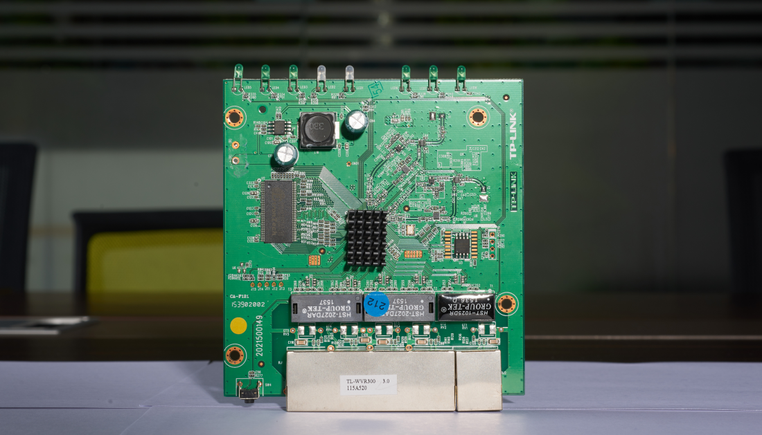
Surface Mount PCB Assembly is a manufacturing process that uses Surface Mount Technology (SMT) to directly attach leadless or short-lead electronic components to the surface pads of a Printed Circuit Board (PCB). This method eliminates the need for drilling holes required by traditional through-hole technology. It achieves this through a continuous automated workflow including solder paste printing, precise component placement via automated pick-and-place machines, and curing in a reflow oven.
The process offers significant advantages such as high assembly density, compact size, reduced weight (40%-60% smaller volume and 60%-80% lighter weight), enhanced reliability, superior high-frequency performance, and 30%-50% lower production costs. This technology serves as the core solution for modern electronics to achieve miniaturization, high-density integration, and scalable production.

What Are Advantages of SMT PCB Assembly Services?
Advantages of Surface Mount PCB Assembly Services:
- High-Density Integration for Enhanced Performance: SMT enables dense placement of leadless components (e.g., 0201, 0402 packages) on limited PCB area, reducing product size by 40-60% and weight by 60-80%. This supports miniaturization demands in smartphones and wearables, delivering “compact yet powerful” solutions.
- Cost Reduction Through Automation: Automated solder paste printing, high-speed pick-and-place machines, and reflow ovens streamline production, cutting unit costs by 30-50% and doubling efficiency. Ideal for high-volume orders in consumer/automotive electronics, directly lowering client procurement expenses.
- Superior High-Frequency Performance: Direct surface-mounting minimizes signal path length, reducing high-frequency loss. Critical for 5G modules and RF devices requiring signal integrity, ensuring reliable communication quality.
- Increased Reliability with Lower Failure Rates: Precision reflow soldering strengthens solder joints by 3-5x, enhancing vibration/thermal resistance. Extends MTBF by 20-50%, reducing client maintenance costs and brand risks.
- Design Flexibility for Rapid Iteration: Supports flexible PCB substrates and custom component layouts, accommodating smart hardware/medical device customization. Enables rapid prototyping and small-batch trials, accelerating time-to-market for competitive advantage.
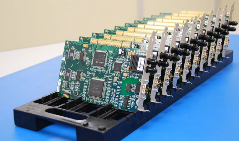
What Are Applications of Surface Mount PCB Assembly?
Applications of Surface Mount PCB Assembly:
- Consumer Electronics: Miniaturized integration in smartphones/TWS earphones/smartwatches.
- Automotive Electronics: High-reliability operation for automotive ECU/ADAS radar/BMS battery management systems.
- Medical Devices: High-precision assembly for portable ultrasound devices/implantable pacemakers.
- 5G Communication: High-frequency signal transmission (28GHz) in base station power amplifier modules.
- Industrial Control: Vibration-resistant and stable operation for PLC controllers/servo drives.
- Aerospace: Extreme environment adaptation for satellite payload boards/spacecraft power modules.
Surface Mount PCB Assembly Process
Step 1: Material Preprocessing and Baking Preparation
- Incoming Material Inspection: Confirm that BGA/PCB, FPC, sensitive ICs (e.g., BGA), and LED beads meet design specifications, with no physical damage or oxidation traces.
- Baking Treatment: All FPC, sensitive ICs, and LED beads must undergo baking before assembly to remove moisture and prevent soldering bubbles or cold joints. Baking temperature is typically 125℃±5℃ for 2-4 hours, adjusted based on material temperature resistance.
Step 2: Solder Paste Management and Printing Process
- Storage and Temperature Recovery: Solder paste must be stored in a 2-10℃ constant-temperature environment. Before use, it requires 4 hours of temperature recovery to room temperature to avoid quality degradation due to temperature differences. After recovery, manual stirring for 3 minutes ensures uniform consistency without clumping.
- Printing and Inspection: Solder paste is printed onto PCB pads via stencil. Post-printing, SPI (Solder Paste Inspection) equipment checks height, area, volume, and detects defects like shorts or offsets to ensure even pad coverage.
Step 3: Component Placement and Reflow Soldering
- High-Speed Placement: SMT machines precisely place BGA, QFN, 0201, and other micro-components onto designated PCB positions with placement accuracy ≤±0.05mm, ensuring no positional deviation.
- Reflow Soldering Process: Placed components enter the reflow oven for a 7-8 minute temperature-controlled cycle (ramp-up-soak-reflow-cooldown). Peak temperature is controlled at 235-245℃ to form robust, void-free solder joints.
Step 4: Post-Reflow Quality Inspection and Defect Screening
- Post-Reflow Visual Inspection: Manual or AOI (Automated Optical Inspection) checks solder joint appearance for issues like insufficient solder, cold joints, or bridges.
- X-Ray Inspection: For PCBs with BGA packages, X-Ray testing verifies BGA solder ball integrity—no voids, offsets, and ≥75% solder coverage.
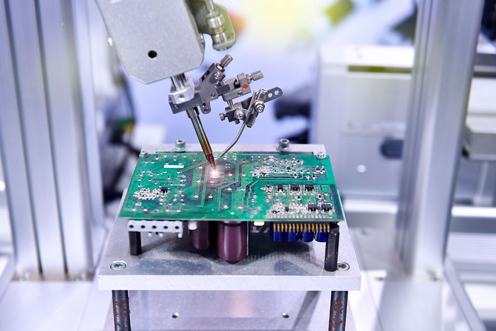
Step 5: Post-Soldering Processing and Functional Verification
- Manual Soldering for Through-Hole Components: Hand-soldering for through-hole components (e.g., connectors, high-power devices) ensures mechanical strength and reliable electrical connections.
- Cleaning and Testing: Ultrasonic cleaning removes flux residues. Subsequent burn-in (firmware programming) and functional testing (electrical performance, signal integrity) validate product compliance with design specifications.
Step 6: Protective Coating and Final Assembly
- Conformal Coating Application: A uniform layer of conformal coating (25-50μm thickness) is sprayed onto the PCB surface to protect against moisture, dust, and corrosion.
- Adhesive Application and Assembly: Adhesive is applied to critical areas (e.g., connectors, interfaces) for reinforcement. Final assembly includes housing installation, labeling, and structural stabilization.
Step 7: Panel Separation, Packaging, and Shipment Preparation
- Panel Separation and Cutting: V-CUT or laser separation machines split PCB panels into individual boards, ensuring smooth, burr-free edges.
- Packaging and Shipment: Products are packaged in blister trays, card dividers, static shielding bags, or bubble wrap based on product characteristics. Labels include model, batch, and environmental compliance marks. Anti-static and shock-resistant packaging ensures safe transport, with shipment prepared per customer requirements.
Quality Inspection of SMT Circuit Board Assembly
1. Incoming Material Inspection (IQC)
- Component Appearance Inspection: Verify that surface-mount components (e.g., chips, resistors, capacitors) are free from damage, oxidation, bent leads, or contamination. Packaging should be intact with clear labels (model, batch, production date).
- Dimensional & Tolerance Verification: Use calipers, microscopes, or vision measurement systems to confirm component dimensions (e.g., package size, lead pitch) comply with specification sheets, preventing assembly defects due to dimensional deviations.
- Batch Consistency Testing: Conduct sampling tests on components from the same batch to ensure electrical parameters (e.g., resistance, capacitance, chip functionality) meet design specifications, avoiding inter-batch variations affecting quality.
2. SMT Placement Process Control
- Placement Accuracy Validation: Utilize high-precision vision systems (e.g., SPI) to verify component placement positions are within tolerance (typically ±0.1mm), preventing welding issues caused by misalignment, rotation, or flipping.
- Solder Paste Printing Quality: Employ SPI to inspect solder paste thickness, uniformity, shape (height/area), and positional accuracy, ensuring no bridges, missing prints, shifts, or slumping.
- Placement Pressure & Speed Optimization: Adjust machine parameters (nozzle pressure, placement speed) based on component type (e.g., QFP, BGA) to avoid damage from excessive pressure or insufficient adhesion from low pressure.
3. Soldering Quality Assessment (Reflow Soldering)
- Solder Joint Visual Inspection: Use manual inspection or AOI to confirm solder joints are smooth, full, and free from defects (cold solder, bridges, solder balls) per IPC-A-610 standards.
- X-ray Inspection: Perform X-ray testing on hidden solder joints (e.g., BGA, CSP) to verify integrity, voids, shorts, or opens for reliability.
- Reflow Profile Validation: Monitor the reflow oven’s temperature profile (preheat, soak, reflow, cooling) via data loggers to ensure compliance with component/solder process requirements (peak temperature, ramp rate), preventing defects from abnormal thermal cycles.
4. Functional Testing & Reliability Verification
- In-Circuit Testing (ICT): Use bed-of-nails or flying probe testers to verify electrical parameters (open/short circuits, resistance, capacitance, inductance) and ensure functional compliance.
- Environmental Stress Testing: Conduct high/low temperature, humidity, vibration, or HALT/HAST tests to validate reliability under extreme conditions and uncover latent defects.
- Performance Verification: Test electrical performance (signal integrity, power stability, timing accuracy) using specialized equipment to meet specification requirements.
5. Inspection Methods & Tools
- Automated Optical Inspection (AOI): Leverage high-resolution cameras and image processing to detect defects in component placement, solder paste, and solder joints, enhancing efficiency and accuracy.
- Automated X-ray Inspection (AXI): Perform non-destructive testing on hidden solder joints to identify internal defects (voids, bridges, opens).
- Manual Inspection & Sampling: Supplement with human expertise for complex areas or special components, ensuring no defects are missed; use sampling to assess overall quality levels.
What Are Surface Mount PCB Different from Other Solutions?
Assembly Method Innovation:
- Unlike traditional Through-Hole Technology (THT) that requires drilling holes for component leads, Surface Mount Technology (SMT) adopts a “solder paste printing + reflow soldering” process. Components are directly mounted on the PCB surface pads, enabling “hole-free” assembly with over three times higher space utilization. This is ideal for miniaturized devices such as smartphones and wearables.
Micro-Scale Integration Capability:
- SMT supports nano-scale components like 01005 packages (0.4×0.2mm), allowing tens of thousands of components to be integrated on a single board—five times the density of THT. THT, constrained by lead hole sizes, is limited to larger packages like DIP, making it unsuitable for modern “small-size, high-functionality” requirements.
Production Efficiency Leap:
- SMT lines feature high-speed pick-and-place machines (50,000-100,000 components per hour) with fully automated processes (printing, placement, reflow), compressing production cycles to 24-48 hours. In contrast, THT relies on manual insertion and wave soldering, resulting in lower efficiency and higher labor costs, only one-tenth of SMT’s throughput in mass production.
Cost-Effectiveness Advantage:
- While SMT requires higher initial equipment investment (e.g., pick-and-place machines, reflow ovens), its unit costs (materials, labor, energy) are 30-50% lower in volume production. THT, despite simpler equipment, incurs significant waste in labor and materials, leading to higher long-term costs and reduced economic viability.
Reliability and Performance:
- SMT solder joints form metallurgical bonds through reflow, achieving high reliability (yield ≥99.9%) with minimal signal loss in high-frequency applications. THT solder joints have high mechanical strength but are prone to vibration-induced failures and greater signal loss due to lead inductance, making them less suitable for high-speed communication and precision instruments.
Scenario Adaptability:
- SMT dominates high-integration fields like consumer electronics, 5G devices, and medical implants. THT remains relevant in industrial controls, automotive engine modules, and other applications requiring high mechanical strength or power handling. Hybrid assembly (SMT + THT) balances both advantages for complex systems like industrial robots and aerospace equipment.
Environmental and Process Compatibility:
- SMT uses lead-free solder paste and nitrogen protection, complying with RoHS standards and supporting both flexible (FPC) and rigid PCBs. THT’s wave soldering generates solder waste and lead pollution, with poor compatibility for thin or irregular boards, posing greater environmental challenges.
Why Choose EBest Circuit (Best Technology) as Surface Mount PCB Assembly Factory?
Reasons Why Choose Us as Surface Mount PCB Assembly Factory:
- Four-Line Synchronized Production Capacity System, 40% Shorter Lead Time: Four fully automated production lines operate in parallel, each with a daily output of 5,000 pieces. MES-driven intelligent scheduling enables 72-hour order response and 5-day urgent delivery, eliminating delays from capacity bottlenecks and reducing client time costs by 40%.
- Nitrogen-Protected Reflow Soldering Process, 50% Enhanced Solder Joint Reliability: German-imported nitrogen reflow ovens maintain oxygen levels below 50ppm. Solder joints achieve ≤3% void ratios and pass AEC-Q100 automotive-grade tests. Third-party validation confirms 1,000 thermal cycles (-40℃~150℃) without failure, cutting post-sale failure rates for automotive/industrial clients.
- High-Precision Placement Technology, Defect Rate Below 0.2%: Yamaha-module-integrated systems handle 01005 components and 0.3mm-pitch BGAs with ±0.05mm accuracy. AI-driven vision calibration (30 checks/sec) ensures zero-offset placement, lifting first-pass yields to 99.8% and reducing rework costs by >30%.
- Full-Process Quality Traceability, Transparent and Verifiable: Each PCBA batch includes encrypted data packages (temperature curves, AOI reports, X-Ray images, material batches). Blockchain storage allows real-time step tracing, meeting medical/aerospace compliance standards.
- Lead-Free Process & Environmental Certifications, Hassle-Free Market Access: Certified to ISO 14001, IATF 16949, and RoHS 2.0, the facility uses lead-free solder and nitrogen protection. Compliance with EU/US regulations boosts export approval rates by 20%, avoiding client compliance costs.
- Dual-Inspection System, 60% Reduced After-Sales Costs: AOI optical checks and X-Ray scanning achieve 99.9% defect interception. A consumer electronics client cut annual maintenance costs by $250K after adoption, minimizing market-distributed defects.
- Low-Temperature Soldering, Reduced Performance Degradation of Sensitive Components: 217℃ nitrogen-enabled soldering prevents thermal damage to MCUs/MEMS sensors. Independent tests show 15% improved signal accuracy retention and 2-year extended product lifespan.
- Intelligent Material Management, Zero Risk of Component Errors: Barcode tracking and AI-managed storage automate BOM-material matching, achieving zero error rates. This eliminates batch scrap from mismatched components, safeguarding client timelines/costs.
Our Surface Mount PCB Assembly Capabilities
| Item | Capabilities |
| Placer Speed | 13,200,000 chips/day |
| Bare Board Size | 0.2″ × 0.2″ – 20″ × 20″ / 22″ × 47.5″ |
| Minimum SMD Component | 01005 (0.4mm × 0.2mm) |
| Minimum BGA Pitch | 0.25mm (10mil) |
| Maximum Components | 50mm × 150mm (Board Area) |
| Assembly Type | SMT / THT / Mixed Assembly |
| Component Package | Reels / Cut Tape / Tube / Tray / Loose Parts |
| Lead Time | 1 – 5 days (Standard) |
How to Get a Quote for Surface Mount PCB Assembly Service?
All Materials for SMT PCB Assembly Quote:
- Gerber Files: Complete PCB layer data (pads, solder mask, silkscreen, stencil layers, etc.), drilling files, stack-up structure, and surface finish specs (e.g., HASL, OSP).
- Bill of Materials (BOM): Excel/standard format listing component details: MPN, brand, package size, reference designator, quantity, supplier. Note special parts (e.g., BGA, 0201) or alternative options.
- Pick-and-Place File: Machine-readable coordinates, rotation angles, and polarity markers for each component.
- Process Specifications: Define special requirements (e.g., lead-free soldering, conformal coating), solder paste type, reflow profile parameters, and non-standard package handling (e.g., QFN, CSP).
- Test Requirements: Functional test plans, electrical test criteria (ICT, AOI), burn-in conditions (e.g., temperature/humidity). Include test point maps and pass/fail standards.
- Quantity & Lead Time: Total order volume, batch splits, delivery dates. Specify if small batches (<100 pcs) allow panelization or urgent surcharges (e.g., +50% for 24h turn).
- Physical Sample/Reference: Prototype or 3D model to validate assembly fit, structural compatibility, and functional alignment.
- Special Requests: Compliance (e.g., RoHS), packaging (ESD bags), logistics (delivery windows), traceability (batch tracking), or engineering support (e.g., firmware flashing).
Welcome to contact us if you have any request for surface mount PCB assembly: sales@bestpcbs.com.