

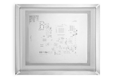
What is an SMT Stencil?
An SMT Stencil (Surface Mount Technology Stencil) is a precision tool used in PCB assembly to deposit accurate amounts of solder paste onto specific pads of a printed circuit board. This tool acts as a template, ensuring solder paste is applied only where needed for component mounting. The SMT Stencil is a core component of the SMT printing process, directly impacting soldering quality and production efficiency.


Key Functions of SMT Stencils in PCB Assembly
Why Is an SMT Stencil Indispensable?
- Controls solder paste volume: Delivers exact quantities to prevent insufficient soldering or bridging.
- Ensures positional accuracy: Aligns with PCB pads to avoid offset paste application.
- Boosts production speed: Enables uniform, rapid paste printing for mass assembly.
- Supports diverse components: Adapts to fine-pitch parts (QFP, BGA) and small chips (0201).
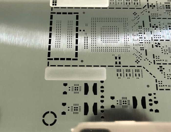
Common Types of SMT Stencils
Which Type Fits Your Project?
| Stencil Type | Key Features | Ideal Applications |
|---|---|---|
| Laser Stencil | ±4μm accuracy, trapezoidal apertures | Fine-pitch components, high-precision PCBs |
| Electropolished (E.P.) Stencil | Smooth hole walls, reduced wiping frequency | QFP, BGA, CSP with ultra-fine spacing |
| Step Stencil | Variable thickness on one stencil | PCBs with mixed component solder demands |
| Electroformed (E.F.) Stencil | Custom thickness, superior smoothness | uBGA, 0201 chips, ultra-dense PCBs |
SMT Stencil Manufacturing Processes: Pros & Cons
Three Main Production Methods
- Laser Cutting: High precision (minimal human error), trapezoidal apertures for better paste release. Cons: Slower production for complex designs.
- Chemical Etching: Fast one-step molding, low cost. Cons: Hourglass-shaped apertures, poor accuracy for fine-pitch parts.
- Electroforming: Smooth hole walls, ideal for ultra-fine spacing. Cons: Long lead time, high cost, environmental impact.
How to Choose the Right SMT Stencil Thickness?
SMT stencil thickness directly determines solder paste volume. For most PCBs, 0.12-0.15mm is standard. Choose 0.08-0.10mm for fine-pitch components (pitch ≤0.3mm) and 0.18-0.20mm for large pads or adhesive printing. Align thickness with component type—BGA typically uses 0.15-0.18mm, while 0201 chips need 0.08-0.10mm.
Critical Guidelines for SMT Stencil Aperture Design
Aperture Ratio & Aspect Ratio Rules
To ensure good paste release, maintain an aspect ratio >1.5 (aperture width/stencil thickness) and area ratio >0.66 (aperture area/hole wall area). For apertures with length <5x width, use area ratio; otherwise, use aspect ratio.
Component-Specific Aperture Tips
- QFP (0.3-0.635mm pitch): Aperture width = 85-90% of pad width, rounded corners to avoid stress.
- BGA: Circular apertures (75-90% of pad diameter) or square apertures for uBGA.
- 0603+ chips: Concave apertures to prevent solder balls and tombstoning.
Materials Needed for SMT Stencil Production
Provide manufacturers with these core materials to ensure accuracy:
- PCB file (Gerber, PCB, DXF, or PDF) with solder paste layer and fiducial marks.
- CAD data (Protel, PowerPCB, AutoCAD) including pad layout and PCB outline.
- PCB sample (if no digital files) to verify pad positions and print surface.
- Special requirements: Step thickness, electropolishing, or nickel plating.
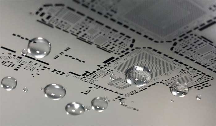
Tips to Improve SMT Stencil Paste Release
- Optimize aperture geometry: Trapezoidal apertures (upper 1-5mil larger than lower) for smooth release.
- Electropolish apertures: Reduces friction between solder paste and hole walls.
- Nickel plating: Enhances surface smoothness, ideal for fine-pitch applications.
- Control stencil tension: Proper tension (30-35N/cm) prevents deformation during printing.
Maintenance & Cleaning of SMT Stencils
Daily Maintenance Routine
- Wipe stencil after 50-100 prints: Use alcohol-based cleaner to remove residual paste.
- Ultrasonic cleaning weekly: Deep clean apertures to avoid paste buildup.
- Inspect for damage: Check for bent frames, torn mesh, or deformed apertures before use.
- Store in dry environment: Prevent rust and contamination of stainless steel surfaces.
FAQ: Common SMT Stencil Issues & Solutions
- Q: Why is solder bridging occurring? A: Reduce aperture width by 5-10%, check stencil alignment, or lower printing pressure.
- Q: Insufficient solder paste on pads? A: Increase aperture size (within ratio limits), thicken stencil, or optimize paste viscosity.
- Q: Paste sticking to stencil apertures? A: Electropolish the stencil, increase wipe frequency, or use a release agent.
- Q: Uneven paste deposition? A: Check stencil flatness, adjust printing speed, or replace worn squeegees.
- Q: Solder balls forming around components? A: Use concave apertures for chips, reduce paste volume, or improve reflow profile.
- Q: Stencil misalignment with PCB? A: Calibrate fiducial marks, check PCB warpage, or adjust stencil frame tension.
How Does SMT Stencil Quality Affect Soldering Results?
Poor SMT stencil quality causes 40% of SMT soldering defects. Inaccurate apertures lead to bridging or insufficient solder; rough hole walls cause paste residue and inconsistent deposition. High-quality SMT Stencils (laser-cut, electropolished) reduce defect rates by up to 70% and improve production yield.
Latest Trends in SMT Stencil Technology
As PCBs become denser, SMT stencil tech evolves: Nickel-plated stencils gain popularity for better paste release; 3D-printed stencils offer rapid prototyping; smart stencils with embedded sensors monitor tension and alignment in real time. These innovations adapt to ultra-fine-pitch components and high-volume production demands.
We provide high-precision SMT Stencil products tailored to your PCB assembly needs, including laser, electropolished, and step stencils. All our stencils comply with IPC-7525 standards and ensure optimal soldering performance. For orders or inquiries, please contact us at sales@bestpcbs.com.