

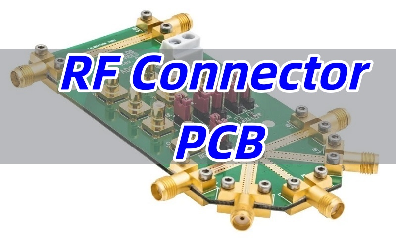
An RF connector PCB is a specialized printed circuit board designed to interface with radio frequency connectors, ensuring stable signal transmission in high-frequency applications. This article provides a comprehensive guide to RF connector PCBs, covering types, materials, layout considerations, and how to select the right components for your needs.
Are you struggling with signal loss, unreliable connections, or delays in sourcing radio frequency boards? Many engineers encounter challenges when integrating RF components into their designs. Common pain points include:
- Impedance mismatch leading to poor signal integrity.
- Difficulty selecting the right PCB material for specific frequency ranges.
- Complexities in RF connector PCB layout causing performance issues.
- Challenges in sourcing mini RF PCB connectors for compact designs.
- Long lead times and unstable quality from suppliers.
Fortunately, these challenges can be overcome with expert manufacturing support. As a specialized RF PCB producer, we address these issues by:
- Implementing precise impedance control techniques.
- Offering a range of high-frequency materials like Rogers and Taconic.
- Providing DFM support for optimal RF connector PCB layout.
- Supplying various mini RF PCB connectors for space-constrained applications.
- Ensuring stable quality and fast delivery through advanced manufacturing processes.
As a reliable RF PCB manufacturer in China, BEST Technology specializes in high-frequency PCB solutions, combining rigorous quality control with rapid turnaround times to meet your project requirements. Whether you require a simple SMA connector PCB prototype or a complex multilayer RF PCB design with stringent impedance control, BEST Technology has the specialized engineering expertise to deliver reliable solutions. Pls feel free to contact us at sales@bestpcbs.com for reliable RF connector PCB solutions.
What is RF Connector PCB?
An RF connector PCB is a PCB engineered to host RF coaxial connectors and provide a controlled-impedance signal transition from the connector to the PCB’s RF traces, ensuring stable high-frequency performance. These boards are engineered to maintain characteristic impedance (typically 50Ω or 75Ω) and minimize signal loss across high-frequency ranges.
- Core Function: The primary role is to provide a stable transition from the PCB’s transmission lines to various PCB mount RF connectors, such as SMA female angle PCB mount RF connector or vertical mount PCB RF connector types.
- Key Characteristics: They feature precise dielectric materials and controlled geometries to preserve signal integrity up to GHz ranges.
- Applications: Commonly used in telecommunications, radar systems, and high-speed data applications.
In summary, the RF connector PCB is a fundamental component in any high-frequency electronic system, ensuring reliable signal transmission between the board and external RF components.
What is the Best PCB Material for RF?
In practical RF PCB applications, designers commonly work within the 500 MHz to 3 GHz range, which covers most wireless communication and IoT systems. Frequencies above 3 GHz generally fall into the microwave domain. Selecting the proper PCB material is crucial for optimal RF performance. The “best” material depends on your specific frequency, loss, and cost requirements.
1. FR-4 for Entry-Level RF Designs (Below ~2.5–3 GHz)
FR-4 can still be used in many low-to-mid RF applications when cost is the priority.
When FR-4 Works Well
• Operating frequency below 2.5–3 GHz
• Short RF trace lengths
• Moderate insertion-loss tolerance
• Consumer-grade wireless products (BLE, WiFi 2.4 GHz, NB-IoT, RFID)
Limitations
• Dielectric constant varies with frequency and temperature
• Higher loss tangent causes signal attenuation in long RF traces
• Not suited for multi-GHz precision RF connectors (e.g., 2.92 mm)
Usage Strategy
Many engineers use hybrid stackups:
FR-4 for non-RF layers + a high-frequency laminate for the RF layer.
2. Rogers Laminates for Stable, Low-Loss RF Structures
Rogers materials are widely considered the industry standard for RF PCBs.
Advantages
- Very stable dielectric constant (Dk):≈ 2.9–3.7
- Very low loss tangent (Df):≈ 0.001–0.003
- Excellent impedance consistency
- Ideal for SMA connectors, IPEX interfaces, micro RF connectors, and other high-frequency transitions.
- Strong performance up to 10–15 GHz, providing significantly more bandwidth capability than typical RF PCB applications require.
Common Grades for RF Connector PCBs
• RO4003C → best cost/performance balance
• RO4350B → higher thermal stability
• RO4835 → oxidation-resistant for higher reliability
Application Scenarios
• LTE, WiFi, GNSS front-ends
• RF connector transition zones(SMA, SMB, 2.92 mm edge-mount)
Rogers is often the first choice for stable-quality RF connector PCBs.
3. Taconic Laminates for Higher-Frequency or Stricter Loss Requirements
Taconic materials perform exceptionally well in microwave and low-mmWave ranges but are also suitable for high-end RF PCBs.
Advantages
• Ultra-low loss tangent
• Strong dimensional stability
• PTFE-based options suitable for precision launch structures
Best Use Cases
• Suitable for microwave applications in the 3 GHz to 10 GHz range.
• Radar, satellite, phased-array antennas
• RF connector regions requiring extremely low VSWR
For regular RF PCB (500 MHz–3 GHz), Taconic is a premium option when you want lower loss than Rogers but can accept higher cost.
4. Isola High-Speed Materials for Mixed RF + Digital PCB Designs
Isola laminated materials are ideal for boards combining RF and high-speed digital.
Advantages
• Good electrical stability up to 6–20 GHz
• Lower cost compared with top-end RF laminates
• More compatible with multi-layer constructions and HDI
Usage Scenarios
• Multi-layer RF/digital mixed systems
• WiFi routers, gateways, small base stations
• Designs requiring balanced performance/cost
5. How to Choose the Best Material for Your RF Connector PCB
The choice depends on your engineering priorities:
Performance Priority
→ Rogers RO4003C / RO4350B
Ultra-Low Loss or Microwave Range
→ Taconic TLX / RF Series
Cost-Sensitive RF Products
→ FR-4 or Hybrid Stackup
Mixed RF + Digital
→ Isola High-Speed Laminates
To sum up, for most RF connector PCB applications within the 500 MHz–3 GHz range, Rogers RO4003C provides the most consistent balance of low loss, stable dielectric behavior, manufacturability, and cost. FR-4 hybrid structures also work well for budget-sensitive designs. Taconic and Isola materials offer elevated performance for more demanding or mixed-signal applications.
What are the Common RF Connector PCB Types?
Various PCB RF connector types are available to meet different mechanical and electrical requirements. Understanding these options helps in selecting the right component for your design.
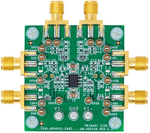
- SMA Connectors PCB: The most common type, including SMA female angle PCB mount RF connector and RP-SMA female adapter PCB edge-mount solder RF connector. Excellent for frequencies up to 18 GHz.
- SMB Connectors PCB: Smaller snap-on alternatives, like the PCB type SMB RF connector, suitable for applications up to 4 GHz where space is limited.
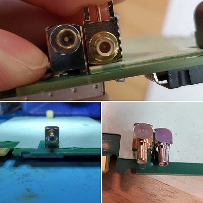
- Miniature Connectors PCB: This category includes mini RF PCB connector and micro RF PCB connectors such as IPEX PCB RF connector, designed for compact devices like smartphones and IoT modules.
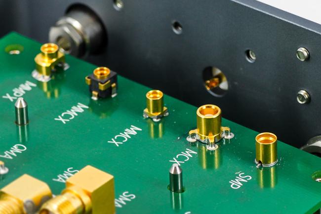
- Edge-Mount Connectors PCB: Such as 2.92 mm edge-mount RF connectors, which require careful attention to PCB thickness for proper mounting and performance.
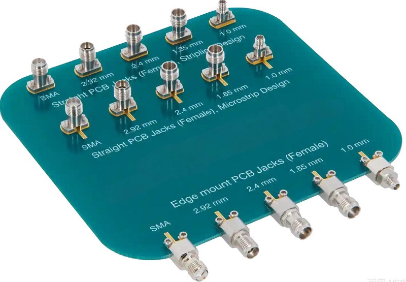
- Stacked and Vertical Options: PCB mount stacked RF connector and vertical mount PCB RF connector save horizontal space on the board.
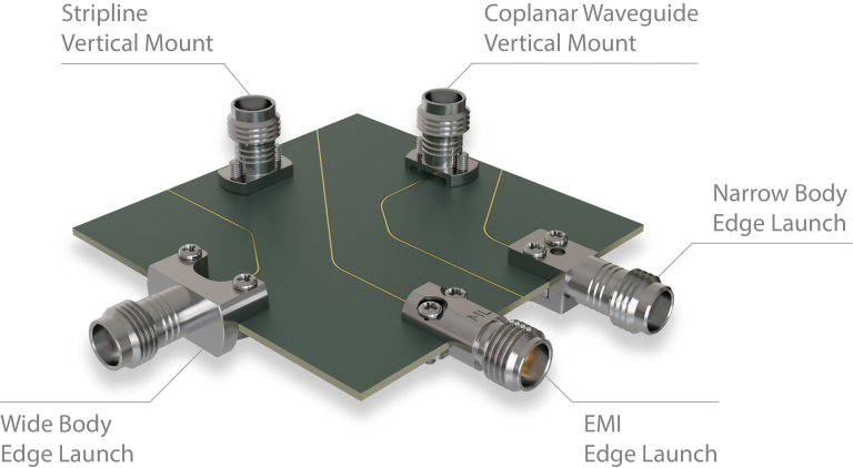
Selecting the correct RF connector PCB type ensures reliable performance and simplifies assembly, contributing to a stable quality RF circuit board. For more information or if you would like to send us any inquiry, please send us an email through the contact form at the bottom of our Contact US Page.
How is the RF Connector PCB Size?
The size of an RF connector PCB is determined by the connector’s footprint, the controlled-impedance transmission line requirements, and the mechanical space needed for reliable assembly. Even a small connector can require a broader PCB area once RF constraints are considered.
1. Connector Footprint and Keep-Out Requirements
Every RF connector—whether a mini RF PCB connector, IPEX, MMCX/MCX, or SMA female angle PCB mount RF connector—comes with a manufacturer-specified footprint.
This footprint defines:
• pad dimensions for the signal and ground pins
• mounting holes (for flange-type connectors)
• mechanical keep-out zones under the connector
• required distance to the PCB edge for edge-mount types
These constraints establish the minimum PCB area around the connector.
2. RF Transmission Line Geometry
The center pin of the connector must transition into a 50-ohm microstrip or stripline.
The trace width depends on:
• PCB material (FR-4, Rogers, Taconic)
• dielectric constant (Dk)
• core thickness above the ground plane
For example, a 1.6 mm FR-4 board may require a 2.5–3.0 mm microstrip width.
This transition also needs space for:
• a tapered pad-to-trace region
• anti-pad clearance
• ground-via fencing along both sides
These RF structures often increase the required PCB width.
3. Mechanical Clearance and Grounding Needs
Additional area is required for:
• connector installation and solder access
• avoiding tall components near the mating area
• dense ground-via rows that provide a low-inductance return path
• optional reinforcement for high-torque connectors like SMA
These mechanical factors further influence the PCB outline.
4. Example: Edge-Mount SMA Connector
Edge-mount SMA connectors illustrate how size is defined by multiple constraints:
• PCB thickness must match the connector specification
• board-edge notches may be required
• wide RF trace transitions need space
• ground-via fences must be placed around the landing area
Thus, even a compact SMA connector results in a relatively wide layout region.
In summary, RF connector PCB size is not fixed—it emerges from a combination of:
• connector footprint
• impedance-controlled RF trace geometry
• mechanical clearance
• grounding and via-fence patterns
The correct approach is always:
Choose the connector → follow its datasheet → calculate RF geometry → build the PCB layout around these constraints.
How to Do RF Connector PCB Layout?
A proper RF connector PCB layout is paramount for minimizing losses and reflections. Here are the key considerations.
- Impedance Matching:
Use controlled impedance routing (typically 50Ω) from the connector pad to the IC.
This requires precise calculation of trace width based on the dielectric constant and thickness of the PCB material.
- Grounding:
Provide an uninterrupted ground plane adjacent to the RF trace.
Use numerous grounding vias around the RF coaxial connector PCB pad to create a low-inductance return path.
- Via Placement:
Minimize the use of vias in the RF path.
When necessary, use via fencing to suppress unwanted mode propagation.
- Component Placement:
Place matching components (like capacitors and inductors) as close as possible to the connector to reduce stray inductance and capacitance.
A disciplined layout approach, often supported by EM simulation tools, is essential for a successful stable quality RF connector PCB.
How to Select Mini RF PCB Connector for Compact RF Modules?
Choosing a mini RF PCB connector for compact modules involves balancing size, frequency, and reliability.
- Frequency Range: Ensure the connector (e.g., IPEX PCB RF connector or micro RF PCB connectors) supports your operating frequency without excessive insertion loss.
- Mating Cycles: Consider the durability required; some miniature connectors have lower mating cycle ratings than full-sized ones.
- Board Real Estate: Evaluate the footprint and height to ensure it fits within the mechanical constraints of your module.
- Assembly Process: Check if the connector is suitable for reflow soldering and compatible with your assembly capabilities.
Selecting the right miniature connector is key to achieving both miniaturization and reliable performance in compact RF designs.
Design Considerations for SMA Female Angle PCB Mount RF Connector in High-Frequency Boards
Integrating an SMA female angle PCB mount RF connector into a high-frequency board requires specific attention to mechanical and electrical details.
- Grounding Connection: Ensure the connector’s outer shell has a robust, low-impedance connection to the board ground plane using multiple vias.
- Board Edge Clearance: For edge-mounted types, maintain the recommended clearance from the board edge to ensure mechanical stability.
- Impedance Continuity: The transition from the connector’s center pin to the PCB microstrip line must be smooth to avoid impedance discontinuities.
- Polarization: Utilize the connector’s polarization key (if available) to prevent incorrect mating during field installation.
Proper design ensures that the SMA female angle PCB mount RF connector performs reliably over its intended lifespan.
Why Choose EBest Circuit (Best Technology) as Your RF Coaxial Connector PCB Supplier?
BEST Technology stands out as your ideal partner for RF coaxial connector PCB manufacturing. Selecting the right partner for RF connector PCB manufacturing is critical for achieving stable high-frequency performance. We deliver a combination of engineering depth, manufacturing capability, and quality assurance that RF projects depend on.
• One-Stop PCB & PCBA Capability:
We provide complete manufacturing services from RF substrate PCB prototyping, fabrication to full PCBA assembly. So your RF connector PCB, matching networks, shielding blocks, and coaxial interfaces are built under one unified process with consistent quality control.
• Specialization in High-Frequency PCB Fabrication:
Our production lines are optimized for RF materials such as Rogers, Taconic, and high-speed Isola, allowing us to meet demanding requirements for dielectric stability, low loss, and controlled impedance across 500 MHz to 3 GHz RF systems.
• Proven Expertise with Multiple RF Connector Types:
We support SMA, SMB, MCX, MMCX, IPEX, mini RF PCB connectors, and precision 2.92 mm edge-mount connectors, ensuring that your design receives the correct footprint, mechanical alignment, and RF launch transition.
• Engineering-Driven RF Layout Support:
Our technical team understands RF connector PCB layout principles—proper pad geometry, via fencing, return-path control, microstrip/stripline transitions—and provides DFM guidance to help customers avoid common RF pitfalls.
• Strict Impedance & Signal Integrity Control:
By using calibrated stackups, impedance modeling, and controlled-etch processes, we maintain consistent 50-ohm transitions from connector pad to RF trace, reducing reflection, insertion loss, and EMI issues.
• Advanced Quality Assurance Built for RF Boards:
AOI, impedance testing, X-ray inspection, and microsection analysis are integrated into our process, ensuring that every RF coaxial connector PCB meets its electrical and mechanical specifications before shipment.
• Fast Turnaround with Stable, Repeatable Quality:
With streamlined RF manufacturing workflows and in-house process monitoring, we deliver stable quality and reliable lead times, enabling customers to accelerate prototype validation and shorten product launch cycles.
• Global Customers Trust Our RF Work:
From wireless communication modules to GNSS front-end boards, radar subsystems, and IoT RF platforms, our RF connector PCBs are used in real-world applications where performance and reliability cannot be compromised.
In a nutshell, an RF connector PCB is the foundation for reliable high-frequency signal interconnection. This guide has explored the key aspects of designing and sourcing these critical components. For your next RF coaxial connector PCB project, partner with BEST Technology for Stable Quality RF Connector PCBs with Fast Delivery. Our expertise ensures your designs perform as intended. A warm welcome to contact us at sales@bestpcbs.com to discuss your requirements.