

Via hole PCB refers to the essential plated interconnect that vertically conducts electrical signals between different layers of a multilayer printed circuit board. This comprehensive guide explores the design, manufacturing, and application of via holes, focusing on their critical role in custom high-density and multilayer PCB designs.
From initial concept to final production, via design presents significant challenges. So, what are the most common frustrations engineers and designers face with PCB via holes?
- Signal integrity degradation from poorly designed vias in high-speed or RF circuits.
- Thermal management failures due to insufficient via stitching under high-power components.
- Manufacturing yield drops and increased costs from pushing beyond standard via hole aspect ratios.
- Reliability issues like via cracking or plating voids during thermal cycling or assembly.
- Difficulty balancing routing density with manufacturable PCB via hole sizes and clearances.
To overcome these hurdles, a partner with deep manufacturing expertise is key. Here are five core solutions we provide for custom via hole PCB challenges.
- We perform in-depth DFM for via holes to ensure your design is both high-performance and manufacturable.
- Our engineers optimize via patterns and PCB via hole filling for superior thermal dissipation in power designs.
- We specialize in controlled processes for high aspect ratio vias, enabling more complex multilayer stacks.
- We utilize advanced plating and plugging techniques to ensure via reliability under thermal stress.
- Our high density PCB capabilities allow for efficient routing with optimal via hole diameters without sacrificing yield.
We are a professional PCB manufacturer specializing in advanced, high-reliability boards. With extensive experience in producing high density PCB with through-hole vias, we excel in turning complex multilayer designs into reality. Our strict process controls, from PCB via hole plating to final electrical test, ensure that every custom via hole PCB meets the highest standards for performance and durability. For your next challenging project, reach out to our engineering team at sales@bestpcbs.com.
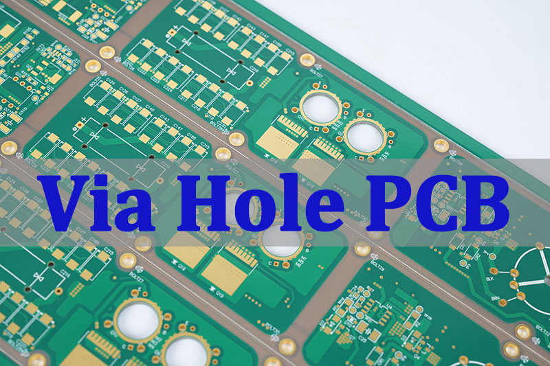
What Is A Via Hole PCB And Why Is It Essential In Multilayer Circuit Design?
A via hole in PCB is a plated-through hole (PTH) that creates an electrical connection between two or more conductive layers in a multilayer board. Unlike a component mounting hole, its primary purpose of via hole in PCB is solely for interconnection. In the context of custom via hole PCB for high-density and multilayer designs, vias are indispensable.
- Enables 3D Routing: They allow traces to escape dense surface areas by moving signals vertically, freeing up real estate on outer layers.
- Forms Layer Transitions: Critical for connecting power, ground, and signal planes across the board stackup.
- Facilitates Miniaturization: Via holes PCB are the backbone of HDI (High-Density Interconnect) technology, allowing for finer pitch components and more complex circuits in a smaller footprint.
- Manages Thermal Paths: Arrays of vias (thermal vias) are used to conduct heat from hot components, like a QFN package’s exposed pad, to internal ground planes or heatsinks.
In summary, without via holes in PCB, multilayer designs would be impossible. They are the vertical highways that make the dense, sophisticated electronics of today feasible.
What Is The Purpose Of Via Hole In PCB For Signal, Power, And Thermal Routing?
The purpose of via hole in PCB varies based on the application, but it fundamentally serves as a conduit. For custom designs, optimizing via use for each purpose is critical.
- Signal Routing Vias: Move high-speed or general signals between layers. Their design (size, stub length) is critical for impedance control and minimizing signal reflection/attenuation.
- Power & Ground Vias: Provide low-impedance paths to deliver stable power and return currents. They are often used in multiples or as part of a via-in-pad design to reduce inductance.
- Thermal Vias: Primarily function as heat pipes to transfer thermal energy from a hotspot (e.g., under a QFN epad) to other layers. Their effectiveness depends on quantity, plating quality, and potential filling.
Here’s a comparison of their primary design goals:
| Via Type | Primary Goal | Key Design Considerations |
|---|---|---|
| Signal Via | Maintain Signal Integrity | Impedance matching, stub management, antipad size |
| Power/Ground Via | Minimize Inductance/Impedance | Multiple vias, proximity to planes, PCB via hole current capacity |
| Thermal Via | Maximize Heat Conduction | Via density, connection to copper planes, filled or plugged vias |
Understanding these distinct purposes of via hole in PCB allows designers to strategically apply them, enhancing both electrical and thermal performance in high density PCB layouts.
What Are The Common Types Of Via Holes In PCB Used In Modern Manufacturing?
Selecting the right type of via hole in PCB is fundamental to successful design. Here are the most common types, crucial for multilayer PCB cross section via hole planning:
- Through-Hole Via: The standard type, drilled through the entire board. Common for DIY PCB copper via through hole but used professionally where layer count isn’t extreme.
- Blind Via: Connects an outer layer to one or more inner layers but does not go through the entire board. Essential for HDI and saving space.
- Buried Via: Connects two or more inner layers without reaching the outer layers. Maximizes surface routing area.
- Microvia: Typically a laser-drilled via with a small diameter (often ≤0.15mm), used in HDI designs. They can be stacked or staggered to create complex interconnects.
- Via-in-Pad: A via placed directly in the component pad. Often filled and capped to prevent solder wicking, saving significant space.
- Filled/Plugged Via: A via whose barrel is filled with conductive or non-conductive material. PCB via hole filling supports via-in-pad designs and can improve reliability.
- Tented Via: A via covered with solder mask to protect it. This is a common, low-cost finish.
For a custom via hole PCB aimed at high density, a combination of blind, buried, and microvias is often employed to achieve the necessary interconnection density while managing layer count and cost.
How To Choose The Right PCB Via Hole Size For Reliability And Cost Control?
Choosing the correct PCB via hole size is a balancing act between electrical needs, reliability, and manufacturing cost. The drill size refers to the finished hole diameter after plating.
- Drill Diameter: Smaller holes allow higher density but are more expensive to drill and plate. A common standard PCB via hole size for through-hole vias is 0.3mm (12mil). Pushing below 0.2mm increases cost.
- Aspect Ratio: This is the board thickness divided by the drilled hole diameter. Higher ratios are harder to plate reliably. Standard processes handle an aspect ratio of ~8:1; advanced processes go higher.
- Pad Diameter (Annular Ring): The copper pad around the hole must be large enough to ensure a reliable connection after drilling misalignment. A minimum annular ring of 0.05mm is typical. You can use a PCB via hole calculator to check this.
- Current Carrying Capacity: The cross-sectional area of the plating determines the PCB via hole current capacity. Larger holes or multiple vias are needed for high-current paths.
- Cost Impact: More drill sizes, smaller holes, and higher aspect ratios all increase fabrication cost. Standardizing on a few hole sizes is economical.
Fundamentally, for a robust 1.6mm thick board, a 0.3mm drill is a reliable, cost-effective choice. For HDI or thicker boards, consult your manufacturer’s capabilities table to select a PCB via hole size that meets your PCB via hole aspect ratio limits.
What Is The Standard PCB Via Hole Aspect Ratio And Why Does It Matter?
The PCB via hole aspect ratio is a critical manufacturing metric defined as:
Aspect Ratio = Board Thickness / Finished Drill Diameter
It matters profoundly because it directly impacts plating quality, reliability, and cost.
- Plating Quality Challenge: During electroplating, the solution must flow into the deep, narrow hole to deposit copper uniformly. A high aspect ratio makes this difficult, leading to thin plating in the center or voids, which can cause PCB via hole crack or open circuits.
- Manufacturing Limit: Each fab has a practical aspect ratio limit. A common standard PCB via hole aspect ratio for reliable production is 8:1 (e.g., a 1.6mm board with a 0.2mm hole). Advanced processes may reach 10:1 or higher for high density PCB.
- Reliability Link: Vias with excessive aspect ratios are prone to plating voids and are more susceptible to cracking during thermal expansion because the thin, weak plating barrel cannot withstand stress.
- Cost Driver: Exceeding standard ratios requires specialized processes (like pulse plating), slower production, and carries a higher risk of scrap, increasing cost.
For a custom via hole PCB, always design within your manufacturer’s recommended aspect ratio. If your design demands a high ratio, discuss it early with your supplier, as it will influence material selection and processing steps.
How Does PCB Via Hole Plating Affect Electrical Performance And Durability?
PCB via hole plating is the thin layer of copper deposited on the hole wall, forming the conductive barrel. Its quality is non-negotiable for both performance and longevity.
Electrical Performance Impacts:
- Resistance: Thinner plating increases DC resistance. Adequate thickness is needed for power vias to handle the required PCB via hole current.
- Inductance: The via barrel acts as a tiny inductor. The PCB via hole inductance is primarily a function of its length (board thickness). While plating has a minor direct effect, poor plating can lead to the use of longer, alternative routing paths.
- Impedance Discontinuity: In high-speed lines, the via’s geometry (including the plating barrel) creates an impedance bump, causing signal reflection. Controlled plating is part of achieving consistent geometry.
Durability & Reliability Impacts:
- Thermal Stress: During assembly reflow, the board and copper expand at different rates. A robust, uniform plating layer resists stress, preventing the PCB via hole crack that can lead to intermittent or complete failure.
- Plating Voids: Gaps or thin spots in the plating are weak points that can initiate cracks or cause high resistance.
- Barrel Fatigue: Over many power cycles, poor plating can lead to fatigue failure.
Therefore, specifying and verifying PCB via hole plating thickness (e.g., 25µm or 1 mil) is essential for ensuring that your custom via hole PCB performs reliably over its intended lifespan.
When Should You Use PCB Via Hole Filling In High-Density Designs?
PCB via hole filling is a process where the empty via barrel is filled with a material after plating. It’s a key technique for custom via hole PCB for high-density and multilayer designs.
You should consider via filling in these scenarios:
- Via-in-Pad (VIP) Applications: This is the most common reason. Filling prevents solder from wicking down the via during assembly, which would starve the component solder joint. The via is then capped and plated over to create a flat, solderable surface.
- Improved Thermal Conductivity: Filling vias under thermal pads (like for QFN epad thermal vias) with conductive epoxy enhances heat transfer from the component into the board.
- Preventing Solder Mask Intrusion: For tented vias, filling provides support for the solder mask bridge, preventing liquid mask from flowing into the hole.
- Enhanced Reliability: Filling can support the via structure, reducing the risk of PCB via hole crack from thermal or mechanical stress, especially for large diameter holes.
- RF/High-Frequency Designs: Filling can help control the dielectric constant around the via, offering slightly more predictable performance.
PCB via hole plugging is a similar but distinct process, often referring to closing the via ends with a non-conductive material without fully filling the barrel. The choice between filling, plugging, or leaving open depends on the specific design goal and should be clarified with your manufacturer.
How Do Through Hole Vias PCB Influence RF And High-Speed Signal Performance?
Through hole vias PCB are necessary evils in multilayer RF and high-speed design. They create unavoidable discontinuities that can degrade signal performance if not managed.
The primary influence of through hole vias on PCB RF performance includes:
- Impedance Discontinuity: The via barrel, its associated pad, and the antipad (clearance in planes) create a local change in impedance, causing signal reflection. This is quantified as a Return Loss penalty.
- Stub Effects: In a via that does not span the full board thickness (e.g., a layer transition), the unused portion acts as a resonant stub. This stub can cause severe attenuation at certain frequencies, a critical issue for multi-gigabit signals.
- Increased Insertion Loss: The conductive path through the via has higher loss than a straight microstrip trace, contributing to overall signal attenuation.
- Crosstalk: Poorly spaced vias can couple energy between adjacent high-speed channels.
Mitigation Strategies for Custom Designs:
- Use Back-Drilling: Remove the non-functional via stub by drilling it out after initial plating. This is highly effective but adds cost.
- Optimize Antipad Size: Enlarging the clearance in ground planes around the via can help tune the local capacitance and improve impedance matching.
- Minimize Via Length: Use the thinnest possible board stackup or blind vias to shorten the via barrel.
- Consistent Return Path: Ensure ground vias are placed adjacent to signal vias to provide an immediate return current path.
Understanding the influence of through hole vias on PCB RF performance is vital. Designers must model these effects (using 3D EM tools) and employ mitigation techniques to ensure signal integrity in high-speed custom via hole PCB designs.
As a final point, via hole PCB is the fundamental vertical interconnect that enables the complex, three-dimensional routing required by modern high-density and multilayer electronic designs. This guide has explored the critical aspects of via design, from types and sizing to the profound impact on electrical and thermal performance.
Mastering via design—understanding the trade-offs in PCB via hole size, aspect ratio, plating, and filling—is essential for creating reliable, high-performance circuit boards. Whether dealing with GHz signals or high-wattage components, the humble via demands careful consideration.
At EBest Circuit (Best Technology), we specialize in navigating these complexities. Our engineering team provides expert DFM for via holes and leverages advanced manufacturing processes to bring your most challenging custom via hole PCB for high-density and multilayer designs to life with reliability and precision. For a consultation on your next PCB via hole project, please contact us at sales@bestpcbs.com.
FAQs
What Does Via Stand For In PCB?
“Via” is not an acronym. It comes from the Latin word for “path” or “way,” denoting its function as a conductive pathway between layers.
What Is The Difference Between Via And Plated Through-Hole?
A plated through-hole (PTH) is a general term for any plated hole, including those used for component leads. A via is a specific type of PTH used onlyfor layer-to-layer electrical interconnection and not for component mounting.
Can You Have Too Many Vias On A PCB?
Yes. Excessive vias can consume valuable routing space, increase manufacturing cost and time, complicate soldering by acting as heat sinks, and potentially weaken the physical structure of the board. They should be used judiciously.
What Does A Via Look Like On A PCB?
On the surface, a via typically appears as a small, round copper pad (the annular ring) with a hole in the center. It may be covered by solder mask (tented) or exposed. You can find many via holes PCB pictures online for reference.
What Are The Different Types Of Holes In PCB?
- Plated Through-Hole (PTH): For components or vias.
- Non-Plated Through-Hole (NPTH): For mechanical mounting or clearance.
- Blind/Buried Via: A PTH that connects internal layers only.
- Microvia: A small, laser-drilled PTH for HDI.
- Countersink/Counterbore Hole: A recessed mounting hole for screw heads.