

Looking for PTH board solution? Explore its definition, components, advantages, production processes, manufacturer selection tips, cost reduction solution, difference between PTH and NPTH board.
As your trusted PTH PCB manufacturing partner, EBest Circuit (Best Technology) delivers exceptional value for international buyers through our unmatched combination of speed, expertise, and cost efficiency. Our 24-hour rapid prototyping service ensures you receive functional samples faster than industry standards, significantly reducing your product development cycle. With 15+ years specializing in PTH board production, we’ve perfected processing techniques for complex designs including high aspect ratio boards (up to 10:1) and mixed-material constructions. Every order includes complimentary DFM analysis by our engineering team – this service alone helps clients reduce production costs by 18-22% through optimized panel utilization and material recommendations. We maintain ISO-certified manufacturing facilities with German-made drilling equipment capable of 0.15mm hole precision, ensuring consistent quality across small batches (10pcs) to mass production (50,000+pcs). Our global supply chain network enables reliable delivery to 37 countries with door-to-door logistics solutions, while competitive pricing (typically 15% below EU/US suppliers) gives you margin advantages in your local market. The combination of speed, technical support, and cost optimization makes us the preferred choice for OEMs and distributors worldwide. Welcome to contact us: sales@bestpcbs.com.
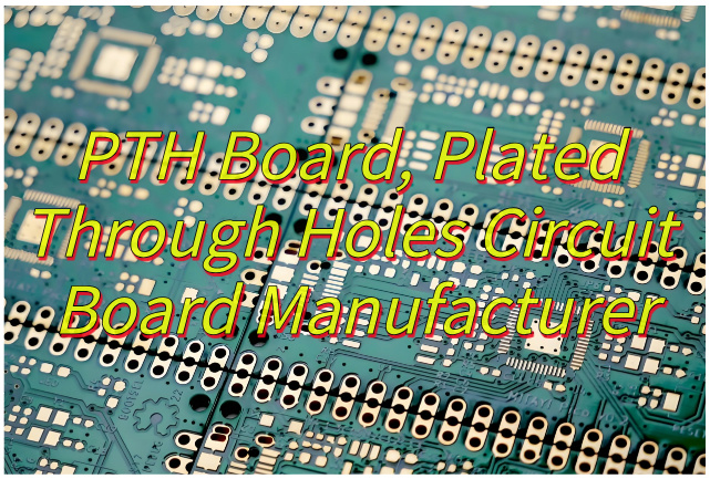
What Is PTH Board?
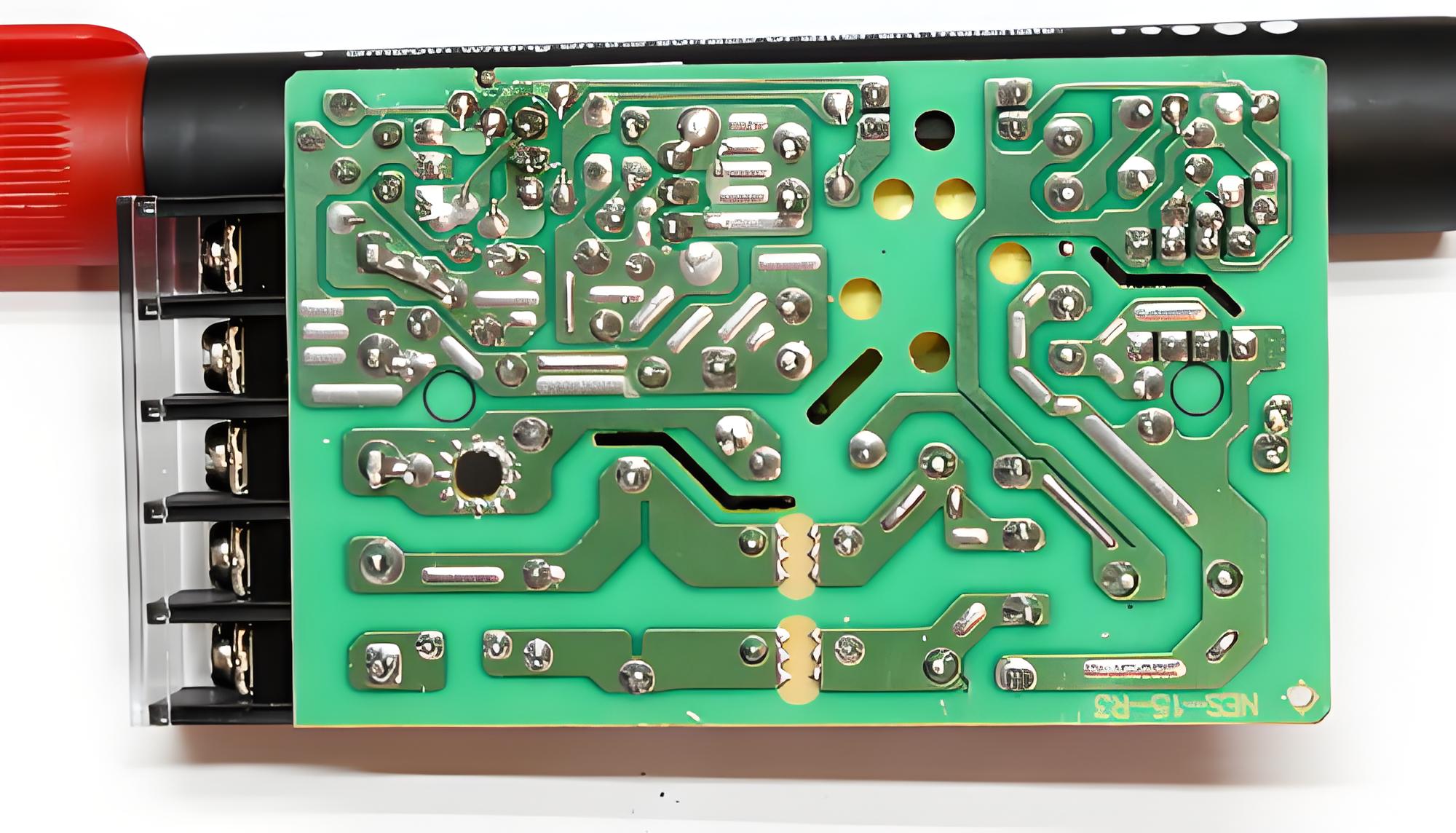
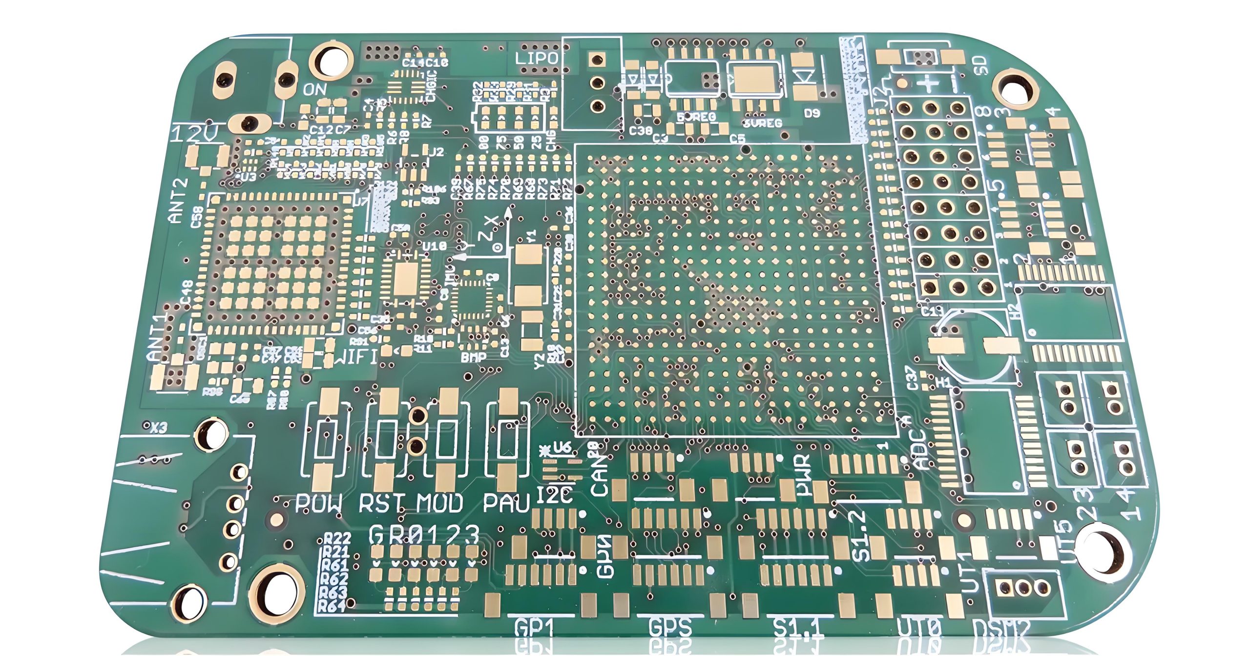
A PTH board, or Plated Through Hole circuit board, is a type of PCB that uses metalized holes to connect conductive layers and surface-mounted components. These holes—drilled through the board’s substrate—are coated with a thin layer of copper, creating electrical pathways between the top and bottom layers, as well as inner layers in multi-layer PCBs. This plating process ensures mechanical stability and low-resistance connections, making PTH boards ideal for applications requiring reliable interconnections, such as high-current circuits, dense component layouts, or devices subjected to physical stress. Unlike Non-Plated Through Hole (NPTH) boards, which use unmetallized holes for mechanical purposes only, PTH boards combine electrical and mechanical functionality, making them indispensable in most commercial and industrial electronics.
What Are Components of PTH Board?
A PTH board consists of several key elements that work together to ensure performance and durability:
- Substrate Material: Typically FR-4, CEM-3, or high-temperature materials like Rogers. The substrate provides mechanical support and electrical insulation.
- Copper Layers: Thin copper foils (e.g., 18μm, 35μm) form the conductive traces and planes on each layer.
- Plated Through Holes: Drilled holes (0.3mm to 3.0mm in diameter) filled with electrolytic copper to connect layers.
- Solder Mask: A protective layer (often green, but available in other colors) that covers non-conductive areas to prevent short circuits.
- Silkscreen Layer: A permanent ink layer for component designators, polarity marks, and other assembly guidelines.
- Surface Finish: Options like HASL (Hot Air Solder Leveling), ENIG (Electroless Nickel Immersion Gold), or OSP (Organic Solderability Preservative) protect copper surfaces for soldering.
What Are Advantages of PTH Board?
PTH boards offer distinct benefits that make them a preferred choice in diverse applications:
- Reliable Electrical Connections: The copper plating in through holes provides low-impedance pathways, critical for high-frequency signals and power delivery.
- Mechanical Strength: Plated holes reinforce component attachment, reducing the risk of solder joint failure from vibration or thermal stress.
- Design Flexibility: Supports multi-layer configurations, allowing complex routing in compact spaces (e.g., 4-layer or 6-layer PCBs).
- Component Versatility: Compatible with both through-hole and surface-mount technology (SMT), enabling hybrid assembly.
- Thermal Performance: Copper plating aids heat dissipation, making PTH boards suitable for power-intensive applications.
- Cost-Effectiveness: Scalable production processes reduce per-unit costs for high-volume orders.
How Do You Make PTH PCB?
Here are manufacturing process of PTH PCB:
1. Design Preparation & Engineering Optimization
Gerber File Finalization:
- Specify hole sizes (0.1mm–6.35mm) with ±0.02mm tolerance for via/component holes.
- Define layer stackup (e.g., 4-layer: signal-ground-power-signal) and surface finish (HASL, ENIG, or immersion silver).
- Include impedance control requirements (e.g., 50Ω±10% for differential pairs).
DFM (Design for Manufacturability) Checks:
- Use Valor NPI software to validate drill-to-copper spacing, annular ring integrity, and solder mask expansion.
- Flag violations for min. trace width (50μm), spacing (75μm), and hole-to-hole pitch (0.2mm).
- Optimize panelization for yield (e.g., 18×24” panels with 24 units per array).
2. Material Cutting & Preparation
Substrate Shearing:
- Cut FR-4 Tg170 or high-TG FR-4 sheets (0.5mm–3.2mm thickness) using CNC shears with ±0.1mm precision.
- Optimize panel size to reduce waste (e.g., 500mm×600mm for automotive controllers).
Pre-Cleaning:
- Degrease panels with alkaline cleaner (pH 12) to remove oxidation before drilling.
3. Precision CNC Drilling
Drilling Parameters:
- Use 0.1mm–3.0mm carbide drills (coated with TiAlN for durability).
- Control spindle speed (80,000–150,000 RPM) and feed rate (0.1–0.5 m/min) to minimize burrs.
Quality Control:
- Measure hole position accuracy with laser micrometers (±0.01mm tolerance).
- Reject panels with >3% broken drills or >0.05mm positional deviation.
4. Deburring & Desmearing
Mechanical Deburring:
- Use nylon brushes (0.3mm bristle diameter) at 200 RPM to remove entry/exit burrs.
Plasma Desmearing:
- Apply oxygen plasma (150W, 2.45 GHz) for 10 minutes to remove resin smear from hole walls.
- Verify cleanliness via SEM imaging (surface roughness <1μm).
5. Chemical Copper Deposition
Catalyst Activation:
- Immerse panels in palladium-tin colloidal bath (50°C, 5 min) to deposit 0.1μm catalytic layer.
Electroless Plating:
- Plate 0.7μm copper using alkaline copper bath (pH 12.5, 75°C) with formaldehyde as reducing agent.
- Monitor thickness via X-ray fluorescence (XRF).
6. Electrolytic Copper Plating
Panel Plating:
- Increase copper thickness to 25–70μm using pulsed current (DC 2A/dm², pulse off 30%).
- Agitate bath with air knives to ensure uniform deposition.
Quality Check:
- Measure via fill ratio via cross-section microscopy (target >95% fill).
7. Image Transfer & Etching
Dry Film Lamination:
- Apply 25μm LPI photoresist at 1.5 m/min speed, 60°C, with 5 kg/cm² pressure.
Exposure & Development:
- Expose using LED UV lamp (365nm, 120 mJ/cm²) and develop in 1% Na2CO3 solution.
Acid Etching:
- Etch copper with cupric chloride (25°C, 2.5 Baumé) at 1.5 m/min speed.
- Achieve <10% undercut via spray pressure control (2.5 kg/cm²).
8. Solder Mask & Silkscreen Application
Solder Mask Coating:
- Apply liquid photoimageable solder mask (LPI) via screen printing (36T mesh).
- Pre-cure at 80°C for 30 min, then UV-expose (800 mJ/cm²) and develop.
Silkscreen Printing:
- Use epoxy ink for component markings (0.15mm line width, 0.2mm height).
- Cure at 150°C for 60 min for adhesion >6N/cm.
9. Surface Finish & Final Inspection
- ENIG Plating: Deposit 1–3μm nickel (electroless) and 0.05–0.1μm gold (electroless) for solderability.
- Electrical Test: Perform flying probe test (100% coverage) for opens/shorts and impedance (TDR).
- AOI & X-ray Inspection: Detect micro-voids and lift-offs using 5MP AOI cameras and 2D X-ray systems.
10. Packaging & Certification
- Vacuum Packaging: Seal panels with desiccant in ESD bags (humidity <5% RH).
- Certifications: Include IPC-6012 Class 3 and RoHS compliance certificates with shipments.
How to Choose A Plated Through Holes Circuit Board Manufacturer?
Selecting a reliable PTH board manufacturer requires evaluating technical capabilities and operational consistency:
- Technical Expertise: Verify experience with PTH processes, including hole filling, copper thickness control, and multi-layer lamination.
- Certifications: Look for IPC-A-600 (Class 2/3), ISO 9001, and RoHS compliance to ensure quality and environmental standards.
- Equipment and Capacity: Check for modern drilling machines (e.g., laser drilling for microvias), automated plating lines, and AOI (Automated Optical Inspection) systems.
- Prototyping Capability: Fast prototyping services (e.g., 24–48-hour turnaround) allow early design validation.
- Quality Control Processes: Inquire about in-process inspections (e.g., copper thickness measurement, cross-section analysis) and final testing (e.g., flying probe tests).
- Cost and Lead Time: Compare quotes for material, tooling, and assembly, ensuring clarity on volume discounts and rush fees.
- Communication and Support: Choose manufacturers with responsive project management to address design revisions or production issues promptly.
How to Maintain Plated Copper Uniformity During the Production Process?
Uniform copper plating in through holes is critical for reliability. Here’s how to achieve consistency:
- Current Density Control: Use controlled rectifiers to maintain optimal current density (e.g., 2–5 ASF) during electrolytic plating, avoiding thin deposits at hole bottoms.
- Additive Management: Introduce leveling agents and brighteners to the plating bath to suppress dendrite growth and ensure even deposition.
- Agitation and Filtration: Agitate the plating solution (via air or mechanical stirring) to enhance chemical flow into holes, while continuous filtration removes particulates.
- Hole Aspect Ratio Consideration: For high aspect ratio holes (depth: diameter >6:1), use pulse plating or specialized additives to improve bottom-up plating.
- Bath Temperature and pH Monitoring: Maintain plating bath temperature (e.g., 25°C–35°C) and pH levels within narrow ranges to stabilize chemical reactions.
- Regular Bath Analysis: Test copper ion concentration, acid levels, and additive concentrations daily to adjust bath composition as needed.
How to Reduce Production Cost of Plated Through Holes Circuit Board?
Cost optimization in PTH board production involves strategic design and process choices:
- Standardize Hole Sizes: Use common drill sizes (e.g., 0.8mm, 1.0mm) to reduce tooling costs and minimize drill bit wear.
- Simplify Layer Count: Avoid unnecessary multi-layer designs; a 2-layer PTH board may suffice for low-complexity applications.
- Choose Through-Hole Only or Hybrid Assembly: Use through-hole components for high-reliability joints and SMT for density, balancing cost and performance.
- Material Selection: Choose FR-4 substrates for standard applications instead of premium materials like Rogers unless required.
- Panelization: Arrange multiple boards on a single panel to reduce setup time and material waste during drilling and plating.
- Negotiate Volume Pricing: Work with manufacturers to secure discounts for large orders or long-term partnerships.
- Minimize Surface Finish Complexity: Prefer HASL over ENIG for non-critical applications to reduce plating costs.
What Is the Difference Between PTH and NPTH PCB?
Below are difference between PTH and NPTH PCB:
1. Hole Functionality
- PTH PCB:The through holes are metalized with copper, serving both electrical and mechanical purposes. They create conductive pathways between different layers of the PCB (critical for multi-layer designs) and provide robust mechanical support for through-hole components, ensuring reliable soldering and stress resistance.
- NPTH PCB:The holes remain unplated and are used exclusively for mechanical purposes. These include mounting holes for screws, alignment pins, or spacers, as well as slots for mechanical fixtures. They do not facilitate electrical connections between layers.
2. Plating Process
- PTH PCB:Requires a specialized plating process: after drilling, holes undergo electroless and electrolytic copper plating to create a conductive layer on the hole walls. This adds complexity but enables interlayer connectivity.
- NPTH PCB:No metalization is applied to the holes. The drilled holes are either left as bare substrate or coated with solder mask for protection, simplifying the manufacturing process.
3. Applications
- PTH PCB:Ideal for most electronic devices where reliable electrical connections and component stability are needed. Common in consumer electronics (e.g., smartphones, laptops), industrial controls, and high-reliability applications like aerospace or medical devices. Supports both through-hole and surface-mount components, making it versatile for complex circuits.
- NPTH PCB:Used in scenarios requiring mechanical precision without electrical functionality. Examples include fixture boards, prototype frames, or structural components where holes are only for mounting or alignment—no signal or power needs to pass through the holes.
4. Cost
- PTH PCB:Higher production costs due to the additional plating steps, specialized equipment, and tighter quality control (e.g., ensuring uniform copper thickness in holes). Suitable for applications where performance justifies the expense.
- NPTH PCB:More cost-effective as it eliminates the plating process. Ideal for low-complexity projects or when holes serve purely mechanical roles, such as simple prototypes or non-electronic structural parts.
5. Design Complexity
- PTH PCB:Supports intricate multi-layer designs with dense routing, as plated holes allow signals to traverse between layers. Requires careful consideration of hole aspect ratio, copper uniformity, and impedance control for high-speed signals.
- NPTH PCB:Design is simpler, focusing on mechanical dimensions (hole size, spacing, alignment) rather than electrical parameters. Less critical for layer stackup or signal integrity, making it faster to prototype.
6. Reliability in Stressful Environments
- PTH PCB:The copper-plated holes enhance mechanical strength, making them more resistant to thermal cycling, vibration, and physical stress—critical for applications exposed to harsh conditions.
- NPTH PCB:Lacks the structural reinforcement of metalized holes, so components attached via NPTH holes may be more prone to loosening or failure under repeated stress.
7. Manufacturing Steps
- PTH PCB:Involves extra processes like desmear (for multi-layer boards), chemical copper deposition, and electrolytic plating, extending production time (typically 3–7 days for prototypes).
- NPTH PCB:Streamlined manufacturing with fewer steps (drilling, deburring, solder mask), enabling faster turnaround times (as quick as 24–48 hours for simple designs).
Conclusion
In summary, a PTH board is a versatile PCB solution with metalized through holes, integrating electrical connectivity and mechanical strength for diverse applications. Its components, advantages, and manufacturing processes demand precision, while choosing the right manufacturer ensures quality and efficiency. Maintaining copper uniformity and optimizing costs are critical for reliability and profitability. Compared to NPTH, PTH excels in electrical performance, making it ideal for complex circuits. By leveraging these insights, you can drive innovation with robust, cost-effective PTH board designs that meet industry standards.