

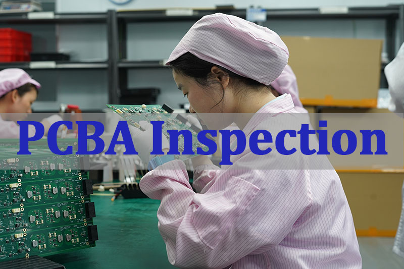
PCBA inspection is the cornerstone of electronics manufacturing, encompassing a suite of processes designed to verify the quality, functionality, and reliability of assembled printed circuit boards. This article explores the critical inspection methodologies that separate high-yield production from costly field failures.
What Are the Biggest Barriers to Consistent PCBA Quality?
- Hidden defects: Solder bridges, insufficient solder, or BGA voids missed by visual checks
- Rework & scrap: Late defect discovery drives repair and warranty costs
- Supplier uncertainty: Limited visibility into a contract manufacturer’s real process control
- Production delays: Manual inspection and testing slow output and launch timelines
- No process feedback: Inspection finds errors but does not prevent repeat issues
How Can a Systematic Inspection Strategy Fix These Problems?
- Multi-stage inspection: SPI, AOI, and AXI catch defects at the source
- Process data control: Inspection data optimizes printing, placement, and reflow
- Clear traceability: Detailed PCBA inspection reports improve transparency
- Efficient test flow: Balanced optical, X-ray, and functional testing avoids bottlenecks
- Closed-loop correction: Real-time feedback enables continuous process improvement
At EBest Circuit (Best Technology), we are a professional PCBA manufacturer committed to delivering high-quality and reliable PCB assemblies. Our investment in state-of-the-art PCBA inspection machines—from solder paste inspection (SPI) and automated optical inspection (AOI) to high-resolution X-ray systems—ensures every board meets the strictest standards. For a quote or to discuss your project’s inspection needs, contact us at sales@bestpcbs.com.
What Types Of PCBA Inspection Are Used In Modern Electronics Manufacturing?
Modern electronics manufacturing employs a layered inspection strategy, where different technologies are applied at various stages to form a comprehensive quality net. This multi-pronged approach is essential for catching a wide spectrum of PCBA defects.
- Solder Paste Inspection (SPI): Applied immediately after stencil printing. A 3D laser scanner measures the volume, height, area, and alignment of deposited solder paste before component placement.
- Automated Optical Inspection (AOI): Used post-reflow (and sometimes post-placement). High-resolution cameras capture 2D or 3D images of the assembled board to check for component presence, polarity, solder joint quality, and basic soldering defects.
- X-Ray Inspection (AXI): Critical for inspecting hidden solder joints. It penetrates components to visualize connections under Ball Grid Arrays (BGAs), chip-scale packages, and within through-hole connectors, identifying voids, bridges, or misalignment.
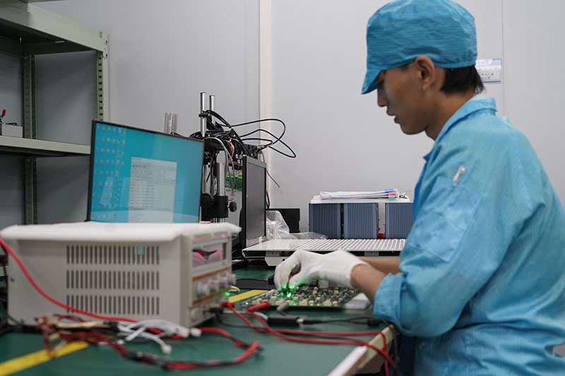
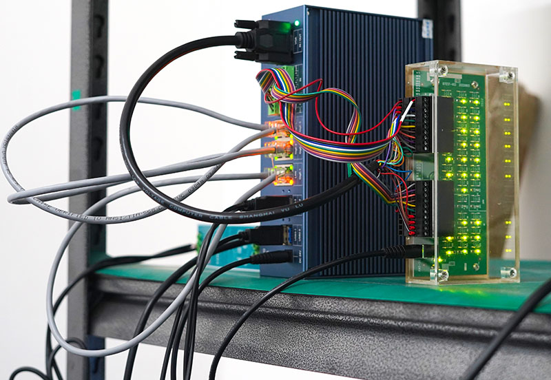
- In-Circuit Test (ICT): An electrical test that uses a bed-of-nails fixture to probe individual nets and components on the powered or unpowered board, checking for shorts, opens, resistance, and capacitance.
- Flying Probe Test: A more flexible electrical test than ICT, using moving probes to access test points without a custom fixture, ideal for lower-volume or prototype runs.
- PCBA Functional Testing: The final validation, where the assembled board is powered and operated in a simulated or real-world environment to verify it performs its intended function correctly.
From process verification (SPI) to structural analysis (AOI/AXI) and final electrical validation (ICT/Functional Test), this cascade of PCBA inspection services ensures defects are identified and corrected at the most cost-effective point in the assembly process.
How Does PCBA Solder Paste Inspection China Improve Assembly Yield?
Solder Paste Inspection (SPI) is the first and most critical automated checkpoint in PCBA production. Because solder paste quality directly determines solder joint reliability, effective SPI directly stabilizes and improves overall assembly yield.
By inspecting solder deposits before component placement, China PCBA solder paste inspection manufacturers prevent printing-related defects from flowing into placement and reflow, where correction becomes expensive and yield loss accelerates.
Key SPI Parameters That Influence Yield
| SPI Parameter | Defects Prevented | Yield Impact |
|---|---|---|
| Paste Volume | Opens, bridges | Stable connections |
| Paste Height | Tombstoning, solder balls | Consistent reflow |
| Paste Area & Alignment | Offset placement | Placement accuracy |
| Paste Registration | Fine-pitch bridging | HDI reliability |
SPI links each measured parameter directly to a specific failure risk and yield outcome, allowing engineers to identify root causes quickly without overloading inspection data with interpretation.
How SPI Drives Real-Time Yield Improvement
SPI is not a final inspection gate. It is a process control tool.
When paste volume trends low or high, operators can immediately adjust stencil pressure, alignment, or cleaning frequency. Because errors are detected before components are placed or reflowed, SPI prevents unnecessary scrap, reduces rework loops, and protects expensive components.
Well-controlled SPI processes routinely reduce printing-related rework and scrap by up to 70%, delivering measurable first-pass yield gains.
Why SPI Is Essential for High-Reliability China PCBA
For any factory delivering high-quality China PCBA, a robust SPI process is non-negotiable. SPI controls the most fundamental variable in soldering: consistent and repeatable solder paste deposition.
Without SPI, downstream AOI, X-ray, or functional testing can only detect failures after value has already been added. With SPI, yield is protected at the earliest possible stage.
What Are The Most Common PCBA Defects Inspection Methods?
Effective PCBA defects inspection relies on matching the right technology to the failure mode. The most common methods form a complementary toolkit.
- Visual Inspection (Manual & Automated):
- Method: Human inspectors or AOI machines examine the board under light.
- Catches: Component absence/misplacement, wrong polarity, visible solder bridges, lifted leads, excessive or insufficient solder (on visible joints), and marking errors.
- Automated Optical Inspection (AOI):
- Method: Cameras capture board images, which are compared to a “golden board” or programmed rules.
- Catches: All visual defects at high speed and consistency. Advanced 3D AOI can also measure solder fillet shapes.
- X-Ray Inspection (AXI):
- Method: Uses X-rays to create an image based on material density.
- Catches: PCBA defects hidden from view: voids in BGA solder balls, insufficient solder under chips, head-in-pillow defects, and alignment issues in QFNs or through-hole joints.
- Electrical Testing (ICT & Flying Probe):
- Method: Probes make physical contact with test points to measure electrical values.
- Catches: Shorts (opens), incorrect component values (resistance, capacitance), missing or wrong components, and faulty diodes/transistors.
- Functional Testing (FCT):
- Method: The board is powered and interfaced with test fixtures/software to simulate real operation.
- Catches: System-level failures, firmware issues, timing problems, and performance parameters outside specification.
While an inspection camera for PCBA (AOI) excels at surface-level checks, a complete strategy requires X-ray for hidden joints and electrical tests for performance validation to ensure comprehensive coverage.
When Should You Use PCBA X Ray Inspection For BGA Assemblies?
PCBA X ray inspection is not always required, but it becomes essential for assemblies where solder joint integrity cannot be verified visually. Its use is dictated by component type, product criticality, and cost of failure.
You should mandate PCBA X Ray inspection for BGA assemblies in these scenarios:
- High-Reliability Products: Medical, automotive, aerospace, or industrial control systems where failure is unacceptable.
- Fine-Pitch or High-Density BGAs: Where solder ball pitch is below 0.8mm, increasing the risk of bridging and making alignment critical.
- Mixed Technology Boards: Assemblies combining BGAs with through-hole or other complex components where thermal reflow is challenging.
- First-Article Inspection & Process Validation: To qualify the stencil design, solder paste, and reflow profile for a new BGA component.
- Failure Analysis & Root Cause Investigation: When a BGA-related fault is suspected, X-ray is the primary non-destructive tool for diagnosis.
Investing in high quality PCBA with BGA X-ray inspection is an insurance policy against latent defects. It provides undeniable proof of solder joint quality beneath the component, ensuring the structural integrity of the most critical connections on the board.
How Does A PCBA Inspection Machine Work In Mass Production?
In mass production, a PCBA inspection machine is a high-speed, automated system integrated into the assembly line. Its operation is a cycle of image capture, analysis, and action.
- Programming: The machine is programmed with the board’s CAD data, creating a “golden” reference model of the correct assembly, including component placement, polarity, and solder joint criteria.
- Board Handling: The conveyor automatically positions the board under the inspection system with precise fiducial alignment.
- Image Acquisition: The system uses its sensors (lasers for SPI, cameras for AOI, X-ray emitter/detector for AXI) to scan the entire board, capturing detailed data points or images.
- Image Processing & Analysis: Sophisticated software compares the captured data against the reference model. It analyzes thousands of features—paste volume, component presence, solder fillet shape, or joint integrity.
- Defect Detection & Classification: The software flags any deviations beyond pre-set tolerances (e.g., “Paste Volume Error – Pad U5,” “Missing Component – R12,” “Solder Void >25% – BGA A1”).
- Result Output & Action: The machine marks the board (e.g., with an ink dot) or sends a signal to the conveyor to route it to a repair or rework station. Simultaneously, it logs all data for Statistical Process Control (SPC), feeding information back to upstream machines (like the printer or placer) for automatic correction.
This automated, data-rich workflow is what makes wholesale offline optical PCBA inspection and in-line inspection viable for high-volume manufacturing, ensuring consistent quality without manual bottlenecks.
What Can An Inspection Camera For PCBA Reveal That AOI Cannot?
While AOI systems are the workhorse of PCBA inspection, a specialized inspection camera for PCBA—often referring to high-magnification manual or semi-automated microscopes—serves a different, vital role. It reveals details that standard in-line AOI is not designed to catch.
- Micro-Scale Defects: Hairline cracks in components or substrates, subtle copper trace damage, or micro-scratches that are below the resolution or contrast threshold of a production-line AOI.
- Material & Texture Issues: Solder discoloration (indicating contamination or thermal stress), flux residue quality, or inconsistencies in conformal coating or potting material.
- 3D Depth & Profile Analysis: While 3D AOI exists, a high-precision inspection camera with depth-from-focus or laser scanning can provide more detailed cross-sectional analysis of specific, complex solder joints.
- Flexible & Non-Standard Angles: Inspecting the sides of tall components, inside connectors, or under overhangs on a flexible PCB assembly, which an overhead AOI camera cannot view.
- Engineering Analysis & Debugging: When a functional test fails, engineers use these cameras to go pro to inspect PCBA areas manually, probe specific points, and diagnose root causes that automated systems may only flag as a general failure.
Think of AOI as the fast, comprehensive patrol officer catching obvious violations, while the specialized inspection camera is the detective examining the forensic details. Both are essential for a complete quality system.
What Does PCBA Functional Testing Verify Beyond Visual Inspection?
PCBA functional testing is the ultimate quality gate, moving beyond the “does it look right?” question of visual/optical inspection to answer “does it work right?”. It validates the assembled board as a complete electronic system.
- Correct System Operation: Powers the board and verifies it boots, communicates, processes inputs, and delivers the correct outputs as per its design specifications.
- Firmware & Software Integrity: Ensures the correct firmware is loaded and functions as intended, which no visual or X-ray inspection can assess.
- Real-World Interface Performance: Tests all interfaces (USB, Ethernet, wireless, audio, display) under load to confirm they meet signal integrity and protocol standards (e.g., following specific USB PCBA inspection guidelines for signal quality).
- Power Integrity & Thermal Performance: Measures current draw, voltage regulation under load, and can monitor for unexpected heating, identifying poor power delivery or shorted components that may pass a static optical check.
- Timing & Synchronization: Validates that processors, memory, and peripherals interact with correct timing, catching issues related to clock signals or high-speed data paths.
While AOI can confirm a memory chip is present and well-soldered, only functional testing can prove it stores and retrieves data correctly. It is the final, critical step in assuring the reliability and performance promised by high-quality and reliable PCB assembly.
Why PCBA Inspection Must Be Built Into The Manufacturing Process?
Treating inspection as a separate, final audit is a costly and reactive strategy. PCBA inspection must be a built-in, integrated element of the manufacturing process to be truly effective for quality control.
- Early Defect Detection = Lower Cost: Finding and fixing a solder paste error with SPI costs pennies. Finding a soldering defect after reflow costs dollars. Discovering it during functional test costs tens of dollars. Finding it in the field costs hundreds in reputation and warranty claims. In-line inspection pushes detection upstream.
- Real-Time Process Control: Inspection data (SPI/AOI measurements) is fed back to printers and placers for automatic parameter adjustment. This creates a closed-loop, self-correcting production line that prevents defect generation, rather than just catching bad boards.
- Data-Driven Continuous Improvement: Aggregated inspection data provides actionable SPC charts. Manufacturers can identify trends (e.g., one nozzle consistently misplaces parts) and perform root-cause analysis to permanently eliminate process flaws.
- Ensures Traceability & Accountability: When each board is linked to its inspection data at every stage, full traceability is achieved. This is critical for industries with strict compliance requirements and for resolving any quality disputes.
- Builds Confidence & Enables Scalability: A robust, embedded inspection framework provides undeniable proof of process capability. It gives brands confidence in their China PCBA solder paste inspection factory partner and allows for seamless, quality-consistent scaling of production.
Ultimately, integrated inspection transforms quality from a hoped-for outcome into a predictable, measurable, and controllable output of the manufacturing process itself.
PCBA inspection is the multi-faceted discipline that safeguards the functionality and longevity of every electronic device. From solder paste validation to X-ray analysis of hidden joints and final functional verification, a layered inspection strategy is non-negotiable for high-quality and reliable PCB assembly.
At EBest Circuit (Best Technology), our manufacturing philosophy is built on this principle. We integrate advanced SPI, AOI, and PCBA X-ray inspection technologies directly into our SMT lines, supported by comprehensive functional testing protocols. This commitment ensures we deliver assemblies you can trust, backed by transparent data and proven process control. For a technical discussion tailored to your specific application, contact our team at sales@bestpcbs.com.
FAQs
What’s the difference between PCB and PCBA?
A PCB (Printed Circuit Board) is the bare, unpopulated board with just the copper traces and laminate. PCBA (Printed Circuit Board Assembly) refers to the completed board after all electronic components (resistors, chips, connectors, etc.) have been soldered onto it.
What are the problems with PCBA?
Common PCBA defects include solder bridges (shorts), insufficient or missing solder (opens), misaligned or tombstoned components, wrong parts, reversed polarity, and solder voids—especially under BGA chips. Electrical issues like shorts and opens are also frequent problems.
What is PCBA used for?
PCBA is the foundational, functioning “brain” or “nervous system” of virtually every modern electronic device, from smartphones and laptops to medical equipment, automotive systems, and industrial controllers.
What is PCBA certification?
PCBA certification refers to compliance with industry quality and reliability standards. Common ones include ISO 9001 (Quality Management), IATF 16949 (Automotive), ISO 13485 (Medical Devices), and IPC-A-610 (Acceptability of Electronic Assemblies), which defines the workmanship criteria for soldering and assembly.