

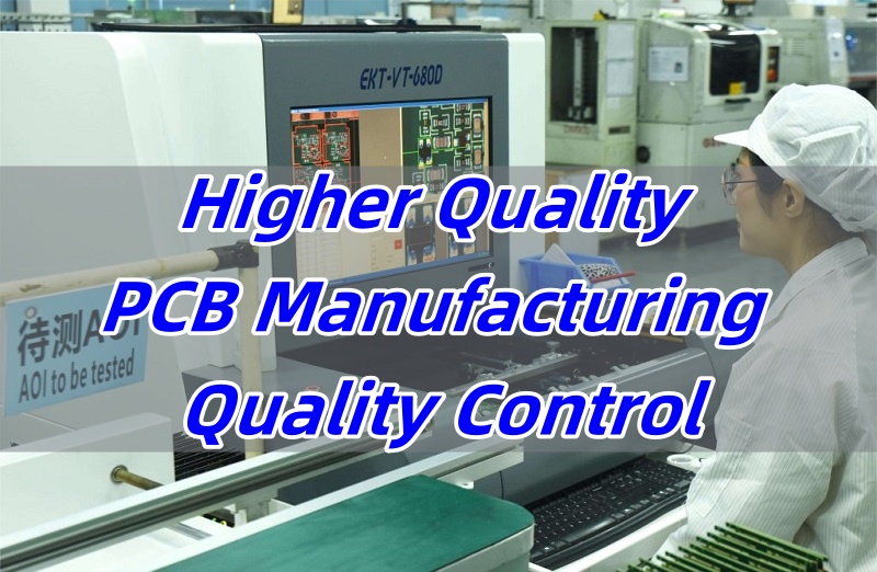
PCB manufacturing quality control is essential for ensuring each board delivers consistent performance in every device it powers. At EBest Circuit (Best Technology), PCB manufacturing quality is the heart of products. We focus on proactive quality management to prevent defects, reduce costs, and increase production yields—especially in high-reliability industries.
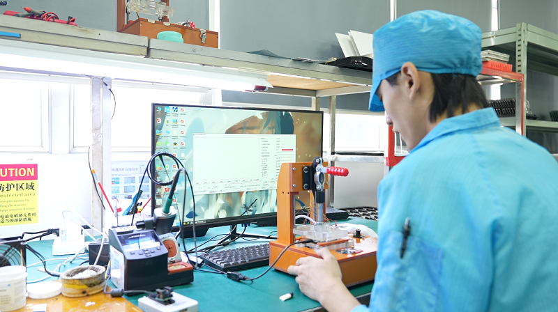
EBest Circuit (Best Technology) provides the most stringent inspection on our PCB and PCBA manufacturing. If you come to visit our workshop, you will find that we have cutting-edge equipment, including Hitachi CNC Control Drill Machine, Automatic PTH Line, E-Tester, Micro Section Photo System, 3D SPI, X-ray, 3D AOI, YAMAHA, and JUKI high-speed pick and place machines, etc. If you have any SMT questions or inquiries, pls share them with us freely. And it would be very nice of you to share your BOM, Silkscreen Reference Designator Diagram, and pick and place coordinates file with us at sales@bestpcbs.com. We are glad to answer any questions you may have and give you our quote as quickly as we can.
What Is PCB Manufacturing Quality Control?
Quality control in PCB manufacturing refers to the checks and measures applied throughout the production process. It ensures that the finished circuit boards meet design, safety, and performance standards. From raw material inspection to final functional testing, each step contributes to preventing failures and protecting end-users.
What Is Included in PCB Manufacturing Quality Control?
PCB manufacturing quality control covers all the critical steps that help prevent defects before boards reach your hands. It starts with checking raw materials and ends with testing the final product. Here’s what’s included:
- Incoming Material Validation
All raw materials—like copper foil, prepreg, and solder mask—are checked to meet required specs before entering the production line. - Process Monitoring
Each stage of production, from drilling to plating to solder mask application, is monitored using MES (Manufacturing Execution System). This ensures consistency and traceability. - In-Line Inspection
High-resolution inspection cameras and innovative AOI systems scan for defects like misalignment, solder issues, or missing features during production. - Post-Production Testing
After fabrication and assembly, PCBs go through electrical tests, flying probe or ICT tests, and visual inspections to confirm functionality and reliability. - Standards Compliance
EBest Circuit (Best Technology) follows global standards like IPC-A-600 and ISO 9001. These help maintain consistency, improve traceability, and reduce rework.
Each of these steps plays a role in building high-quality, failure-free boards that meet customer expectations and perform reliably in critical applications.
What Are the PCB Manufacturing Defects?
PCB defects can occur at different stages of manufacturing and may lead to electrical failure, reliability issues, or costly rework. Here are the most common types:
- Open Circuits
This happens when a trace or connection is broken, often due to poor soldering, damaged pads, or design misalignment. It results in an incomplete electrical path. - Short Circuits
Shorts occur when unintended connections form between two conductors. They are usually caused by solder bridging, excess copper, or design flaws and can lead to overheating or complete failure. - Copper Burrs or Excess Copper
Tiny fragments or extra copper left after etching can create accidental pathways between traces. These are especially risky in high-voltage or high-density designs. - Solder Mask Misalignment
If the solder mask doesn’t align properly with pads or traces, it can expose copper unintentionally or cover pads that should remain open, impacting soldering quality. - Incorrect or Missing Holes
Misdrilled or missing vias and plated through-holes can disrupt electrical continuity and make it difficult or impossible to mount components correctly. - Contamination (Dust or Oil Residue)
Even small particles of dust or oil left during processing can interfere with signal integrity, especially in RF or high-speed boards. - Micro-Cracks and Bridging Defects
These tiny flaws may not be visible with standard inspection tools but can lead to field failures due to thermal stress, vibration, or oxidation over time.
Each of these defects can impact performance, durability, and safety. That’s why strong quality control measures are critical throughout the entire manufacturing process.
What Are the Quality Control Methods for PCB Manufacturing?
EBest Circuit (Best Technology) combines the following control methods to reduce failure rates and improve reliability:
- AI-Driven AOI: Our smart systems detect defects like bridging or missing solder with up to 99% accuracy.
- Predictive Analysis: We use past defect data to stop future issues before production even starts.
- IPC Standards: We follow IPC-A-600 guidelines to reduce rework and increase consistency.
- ISO 9001 Certification: Every process is tracked and improved for traceability and quality assurance. Our factory is fully compatible with ISO 9001, ISO 13485, IATF 16949, AS9100D, UL, REACH, and RoHS.
What Are the Tolerances for PCB Manufacturing?
PCB manufacturing tolerances determine how much deviation is allowed in layer alignment, hole positioning, and conductor spacing. For high-reliability boards, tolerances are strict. At EBest Circuit (Best Technology), we follow IPC Class 2 or 3, depending on customer requirements. For example, hole size tolerances are kept within ±0.075mm, and conductor width tolerance is ±10%.
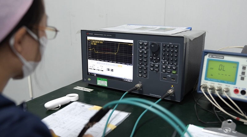
What Are the PCB Manufacturing Tests in Manufacturing PCB Process?
Testing is key to identifying issues before boards leave the factory. We perform the following:
- Flying Probe Test: Detects opens and shorts in prototypes and small batches.
- In-Circuit Test (ICT): Verifies correct assembly and functionality.
- X-ray Inspection: Used for BGAs and hidden solder joints.
- Functional Testing: Simulates real working conditions to catch unseen faults.
How to Check PCB Quality?
Checking PCB quality is not a single step—it’s a layered approach that spans across the entire manufacturing process. At EBest Circuit (Best Technology), we implement inspection and testing checkpoints at key production stages to ensure that every board meets the expected standard before it’s shipped. Here’s how we do it:
- Visual and AOI Inspection (Inner and Outer Layers)
After etching the inner layers, we perform Automated Optical Inspection (AOI) to detect trace breaks, shorts, or pattern defects. Once the outer layers are built, a second AOI check is carried out. These inspections catch surface and structural issues early, reducing scrap and rework. - Drilling and Plating Quality Checks
During the drilling stage, hole diameter and position accuracy are checked. After copper deposition and electroplating, we ensure that plating thickness meets IPC standards and that via integrity is intact—especially for multilayer designs. - Solder Mask Alignment and Thickness Control
Misalignment or inconsistent coverage during solder mask application can lead to exposed copper or covered pads. We verify alignment and thickness using optical systems, helping to prevent electrical leakage and protect signal paths. - Solderability Testing and Surface Finish Verification
Before final testing, we assess solderability—particularly after surface treatment (like ENIG or HASL)—to confirm wetting behavior. This ensures good bonding during assembly and extends shelf life. - 3D SPI (Solder Paste Inspection)
Although primarily used during PCBA, we integrate 3D SPI systems in some projects to validate paste application patterns and volumes, especially for prototype or customer-critical builds. - Electrical Testing
Every board undergoes flying probe testing or fixture-based testing to confirm electrical continuity and isolation. Open or short circuits are flagged and resolved before delivery. - Cleanliness and Ionic Contamination Testing
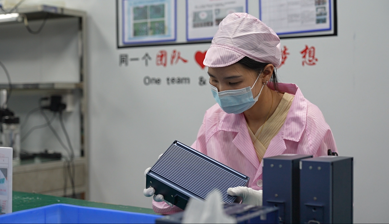
For high-reliability or high-frequency PCBs, ionic contamination is a hidden risk. We use ion chromatography and resistivity testing to check for residues like flux or oil, which can cause signal interference or corrosion over time. - Final Quality Control (FQC)
Before packing, our FQC team performs a final round of checks including dimensional accuracy, edge finishing, surface finish uniformity, and barcode traceability. These checks ensure that the boards meet IPC-A-600 acceptance standards. - Traceable Manufacturing Records
Throughout production—from inner layer exposure to packaging—our MES system records every process and operator involved. This allows complete traceability for root-cause analysis if a defect ever occurs.
Thanks to our sophisticated AOI systems and real-time process control, we’ve reduced false call rates by over 90% and improved critical defect capture close to 99%. For our customers, this means fewer production stops, less rework, and far more predictable board performance.
What Is the Difference Between QA and QC Quality Control?
QA (Quality Assurance) is proactive. It builds quality into the process through planning and system design. QC (Quality Control) is reactive. It finds and corrects issues after or during production. At EBest Circuit (Best Technology), we use both—QA to prevent, QC to detect and fix. This combined strategy cuts failure rates by more than 20% across batches.
Whether you’re producing 100 units or scaling to 100,000+, EBest Circuit (Best Technology) has the tools, teams, and tech to match your needs. Our customers in automotive, aerospace, and medical industries rely on us for consistent quality and proactive problem-solving.
In conclusion, quality doesn’t just protect—it leads. By making PCB manufacturing quality control a strategic priority, companies avoid costly recalls, improve customer satisfaction, and stand out in the most crowded markets. EBest Circuit (Best Technology) helps you reach that goal with advanced inspections, smart data use, and high-reliability materials like graphene-based substrates and high-Tg FR4. We’re here to turn defects into insights and challenges into wins. If you have any questions or need any support, just feel free to reach out to us at sales@bestpcbs.com.