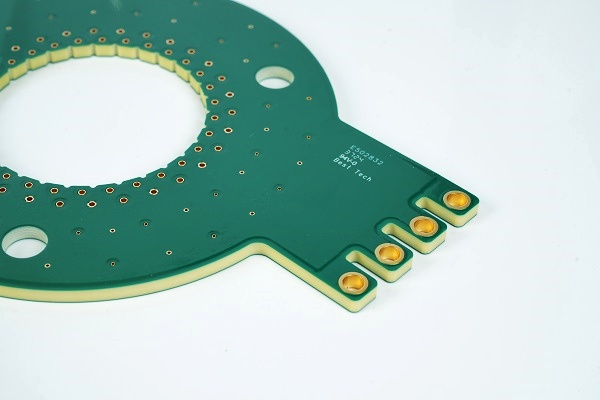
A thick copper PCB refers to a printed circuit board that uses a higher amount of copper than a standard PCB. Typically, standard PCBs have copper thickness ranging from 0.5 oz to 2 oz per square foot. However, when the copper thickness is 3 oz or more per square foot, it is classified as a thick copper PCB.
These boards are built for handling high current, enhanced heat dissipation, and strong mechanical performance. You’ll find them in power electronics, electric vehicles, solar inverters, and industrial machinery—wherever reliability and power handling are critical.
At EBest Circuit (Best Technology), we specialize in custom thick copper PCB manufacturing. Whether you need 3 oz or 20 oz copper, our engineering team supports your design with precision, reliability, and fast delivery. We also provide full traceability and strict quality control, making sure each board meets your performance needs.
Advantages of Thick Copper PCB
1. High Current Carrying Capacity
Thicker copper allows your PCB to carry more current through its traces without causing excess heat. This helps prevent overheating and damage to components. In other words, thick copper gives your board the power capacity it needs to run safely and efficiently.
2. Excellent Thermal Management
Heavy copper spreads heat more evenly across the board and away from sensitive components. This reduces hot spots and helps maintain stable operation. It’s especially useful in environments where heat buildup can be a problem, such as power supplies or LED lighting systems.
3. Increased Mechanical Strength
Thick copper PCBs are more durable. They are less likely to bend, crack, or delaminate during assembly or use. This added strength makes them ideal for heavy machinery, vehicles, and military equipment.
4. Improved Reliability and Product Life
Better current and heat handling reduce stress on the board and components. This leads to longer lifespan and fewer failures, which saves both time and cost in maintenance.
5. Compact and Efficient Designs
You can use narrower traces with thick copper while still meeting your current requirements. This allows for smaller board sizes and space-saving layouts, especially valuable in compact devices.
All of these advantages make thick copper PCBs a smart choice when performance and reliability truly matter.
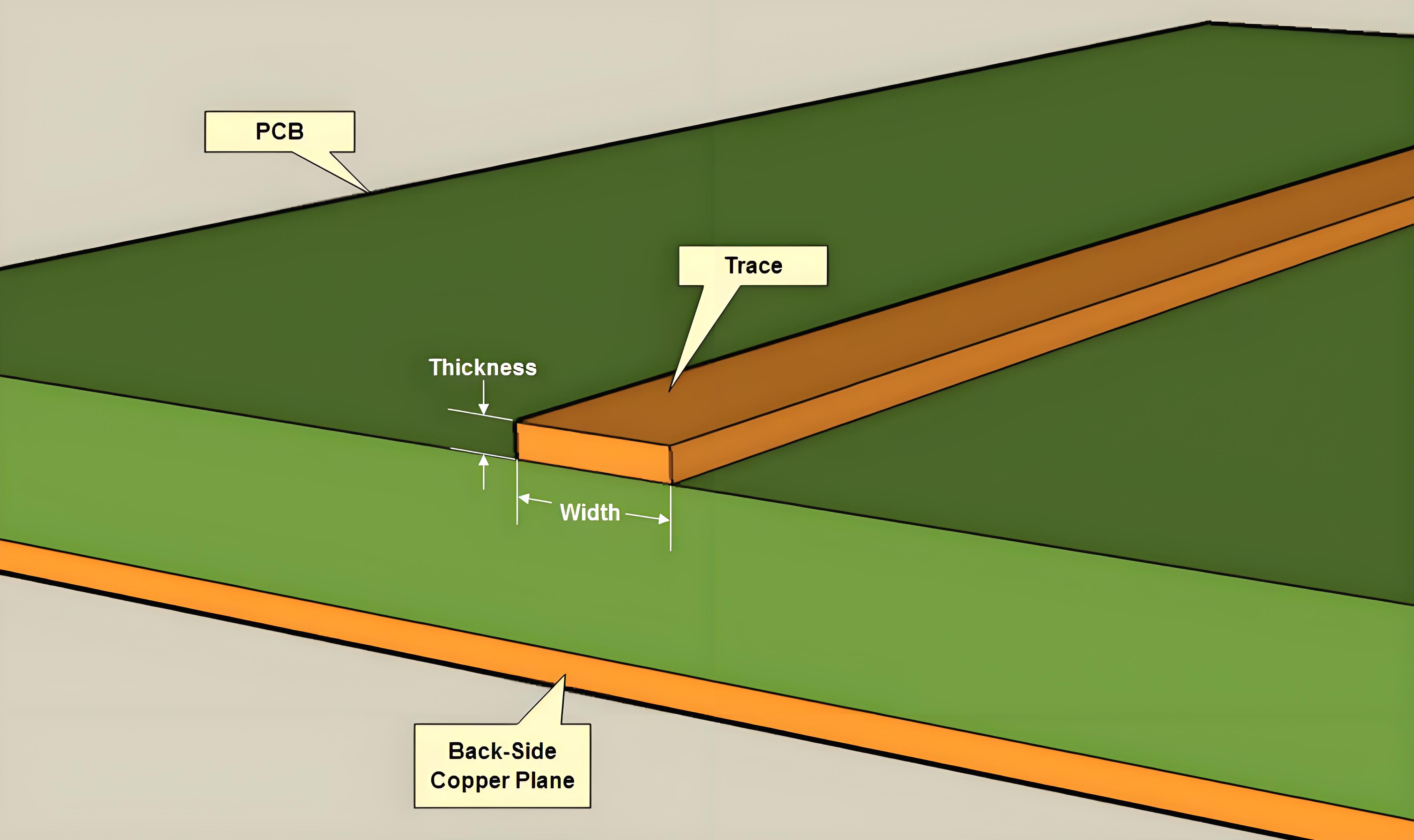
Standard PCB Copper Thickness Chart
Copper thickness is usually measured in ounces per square foot (oz/ft²) or microns (µm). For every 1 oz of copper per square foot, the actual thickness of the copper layer is about 35 microns, or 1.4 mils. To help you understand how thick copper compares to standard copper, here’s a simple PCB Copper Thickness Chart with typical values.
| Copper Weight (oz/ft²) | Thickness (microns) | Thickness (mils) | Common Usage |
| 0.5 oz | ~17 µm | ~0.7 mil | Signal layers, low-power circuits |
| 1 oz | ~35 µm | ~1.4 mil | Most standard PCBs |
| 2 oz | ~70 µm | ~2.8 mil | Power circuits, motor drivers |
| 3 oz | ~105 µm | ~4.2 mil | Start of thick copper PCB range |
| 4 oz | ~140 µm | ~5.6 mil | High-power, heat-intensive applications |
| 6 oz | ~210 µm | ~8.4 mil | Industrial power systems, battery packs |
| 10 oz | ~350 µm | ~14 mil | Heavy-duty, high-current applications |
Whether you are working on a standard 1 oz board or a 10 oz thick copper PCB, the thickness affects everything from electrical performance to thermal control. If you are unsure which thickness suits your project, EBest Circuit (Best Technology) offers expert guidance and custom PCB solutions. We help you choose the right copper weight to match your current load, heat needs, and budget.
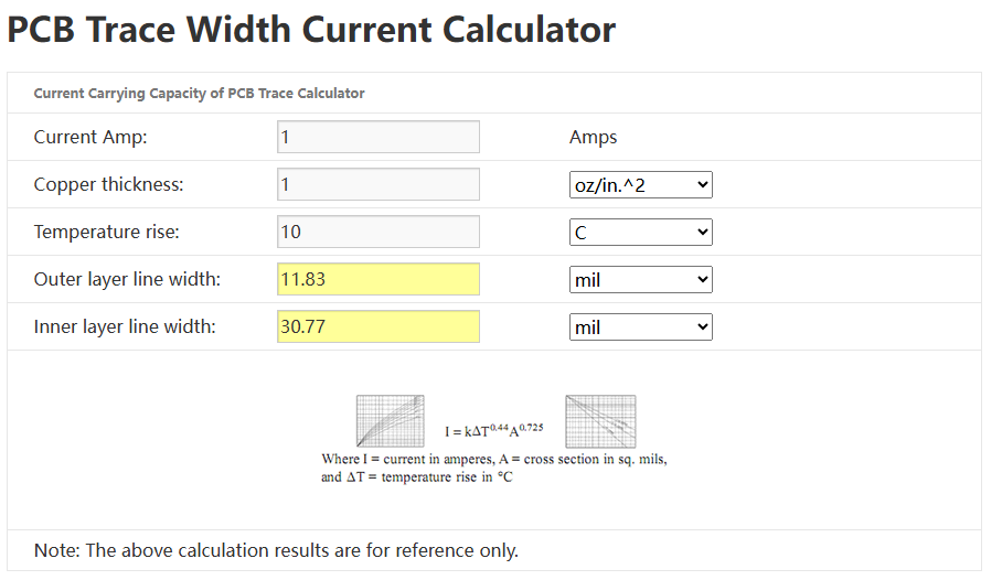
PCB Copper Thickness vs Current
One of the biggest reasons to use thick copper is current capacity. As copper thickness increases, it can carry more current without excessive heating. Here’s how it works:
- 1 oz copper can carry around 1.2A on an inner layer for a 10°C temperature rise.
- 3 oz copper can carry about 3.6A under the same conditions.
- Higher copper weights (like 10 oz) can handle much more, depending on trace width.
This relationship is essential for designing safe and efficient circuits. Using IPC-2221 standards as a guide, engineers can determine how much copper is needed for any given load.
If you’re unsure, tools like the PCB copper thickness calculator can help you find the right copper weight based on your current and design needs.
How to Choose PCB Copper Thickness?
Knowing how to choose PCB copper thickness is essential when designing a board that performs reliably under electrical and thermal stress. The right copper thickness affects current flow, heat management, durability, and even the size of your board. Choosing wisely can improve performance and reduce long-term costs.
1. Understand Your Current Requirements
Start by determining how much current your traces need to carry. Higher current demands thicker copper or wider traces. If your circuit handles heavy loads—like in power supplies or electric vehicles—you’ll likely need thick copper, starting from 3 oz or more.
2. Evaluate Space and Trace Width
Sometimes, there’s limited space on your PCB. If you cannot increase trace width to carry higher current, you can increase copper thickness instead. Thicker copper allows for narrower traces to handle the same current safely, helping you keep your design compact without sacrificing performance.
3. Check for Voltage Drop
Resistance in copper causes voltage drop across traces. Thicker copper has lower resistance, which means less voltage loss. If maintaining consistent voltage is important for your application—like in precision circuits or power regulation—opt for thicker copper to minimize drops.
4. Consider Cost and Board Size
While thicker copper improves performance, it also adds cost and weight. Choose copper thickness that meets your technical needs without over-engineering. For most consumer electronics, 1 oz or 2 oz is enough. For power devices, 3 oz to 10 oz may be needed.
Thick Copper PCB Applications
- Power supplies
- Converters
- Inverters
- Battery systems
- Motor drives, and charging circuits efficiently
- Solar Power Systems
- Inverters and control circuits
- Military and Aerospace
- Industrial Control
Anywhere power, heat, or strength is a concern, thick copper PCBs provide dependable performance.
How to Avoid Thick Copper PCB Delamination?
The delamination of thick copper circuit boards refers to a phenomenon that occurs during PCB manufacturing. Due to insufficient adhesion between the copper foil and the substrate or excessive internal stress, the copper foil and the substrate (such as FR-4 fiberglass board) separate from each other.
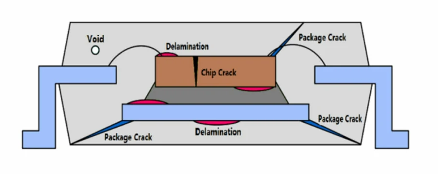
While it’s not common, thick copper PCBs can be more prone to this issue if not manufactured properly. Here are some ways to avoid it:
1. Use High-TG Materials
High-TG (glass transition temperature) materials like FR4-TG170 or ceramic can better resist heat and stress.
2. Reliable Lamination Process
Proper lamination ensures strong bonding between copper and substrate. At EBest Circuit (Best Technology), we use high-pressure lamination and strict process control to prevent delamination.
3. Controlled Soldering Heat
Excessive heat during soldering can damage the board. Controlled soldering ensures minimal thermal stress.
4. Avoid Design Stress Points
Sharp corners and very narrow traces can concentrate stress. A smooth, balanced design reduces risk.
5. Quality Assurance
Choose manufacturers with strong quality systems that include thorough inspection and testing.
Best Thick Copper PCB Manufacturer – EBest Circuit (Best Technology)
Looking for a trusted thick copper PCB manufacturer? Here’s why EBest Circuit (Best Technology) is your best choice:
- We specialize in 3 oz to 20 oz thick copper PCBs.
- Certified with ISO9001, IATF16949, and UL.
- Advanced plating and lamination techniques ensure strength and reliability.
- Fast prototyping and mass production services.
- Competitive pricing and on-time global delivery.
- Engineering support for design, layout, and material choice.
- Full traceability with our MES system and strict quality control.
Need help with your next project? Contact EBest Circuit (Best Technology) today for a custom quote and expert support.
FAQs
1. What copper thickness qualifies as thick copper PCB?
Anything 3 oz per square foot or more is considered thick copper PCB.
2. How do I calculate required copper thickness?
Use a PCB copper thickness calculator based on your current, trace width, and temperature rise.
3. Can thick copper PCBs be multi-layered?
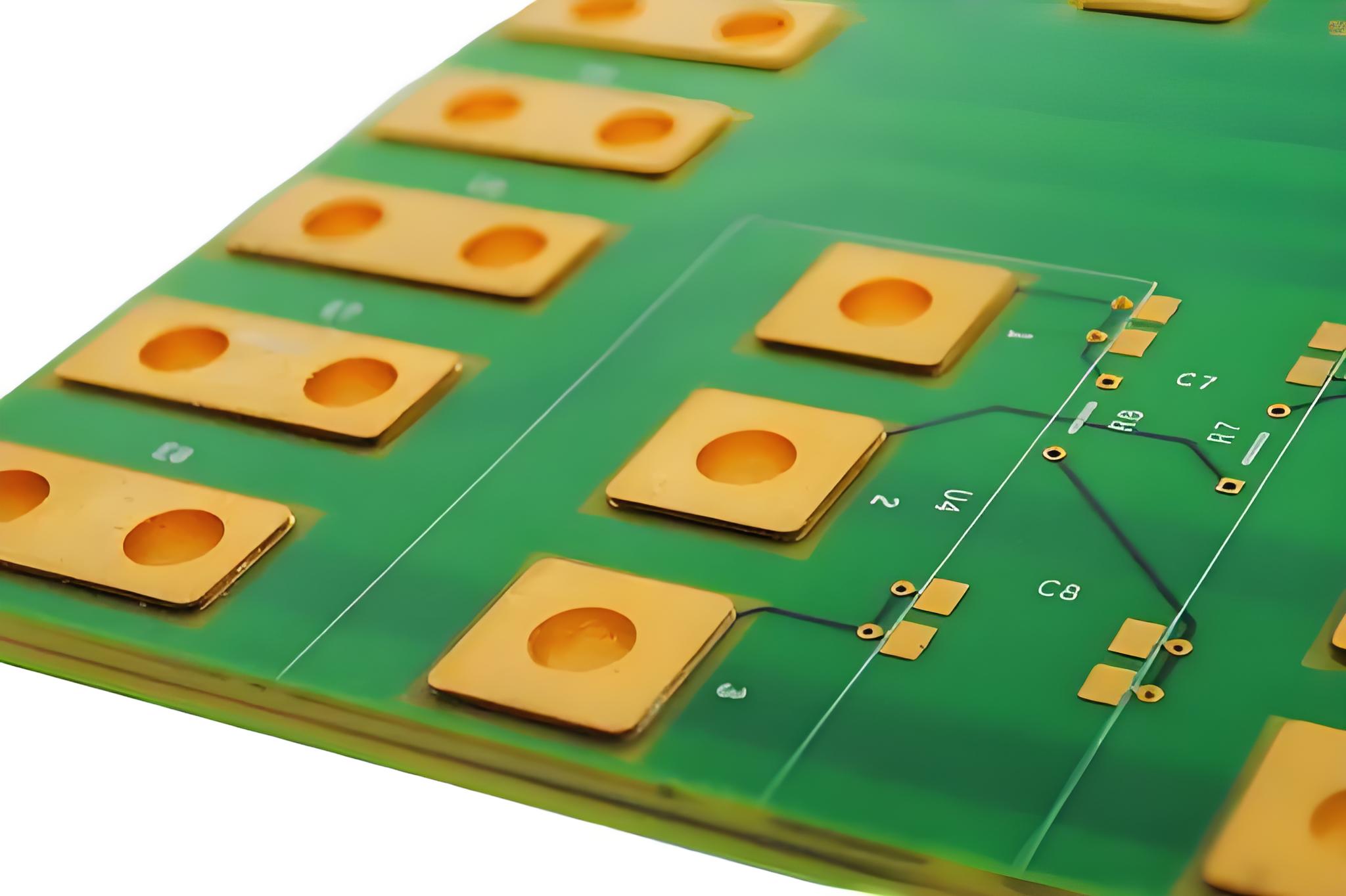
Yes, we manufacture single, double, and multi-layer thick copper PCBs.
4. Do thick copper PCBs cost more?
Yes, but they offer better performance and longer life, which offsets the cost.
5. How do I get a quote from EBest Circuit (Best Technology)?
Just contact us with your design files, and we’ll provide a competitive, customized quote.