

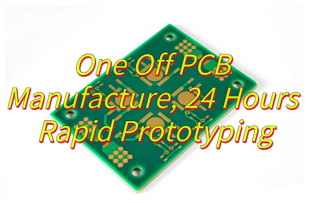
Seeking for one off PCB manufacturing solutions? This guide covers 24-hour turnaround, cost-effective processes, quality assurance, and advanced design capabilities for rapid hardware validation.
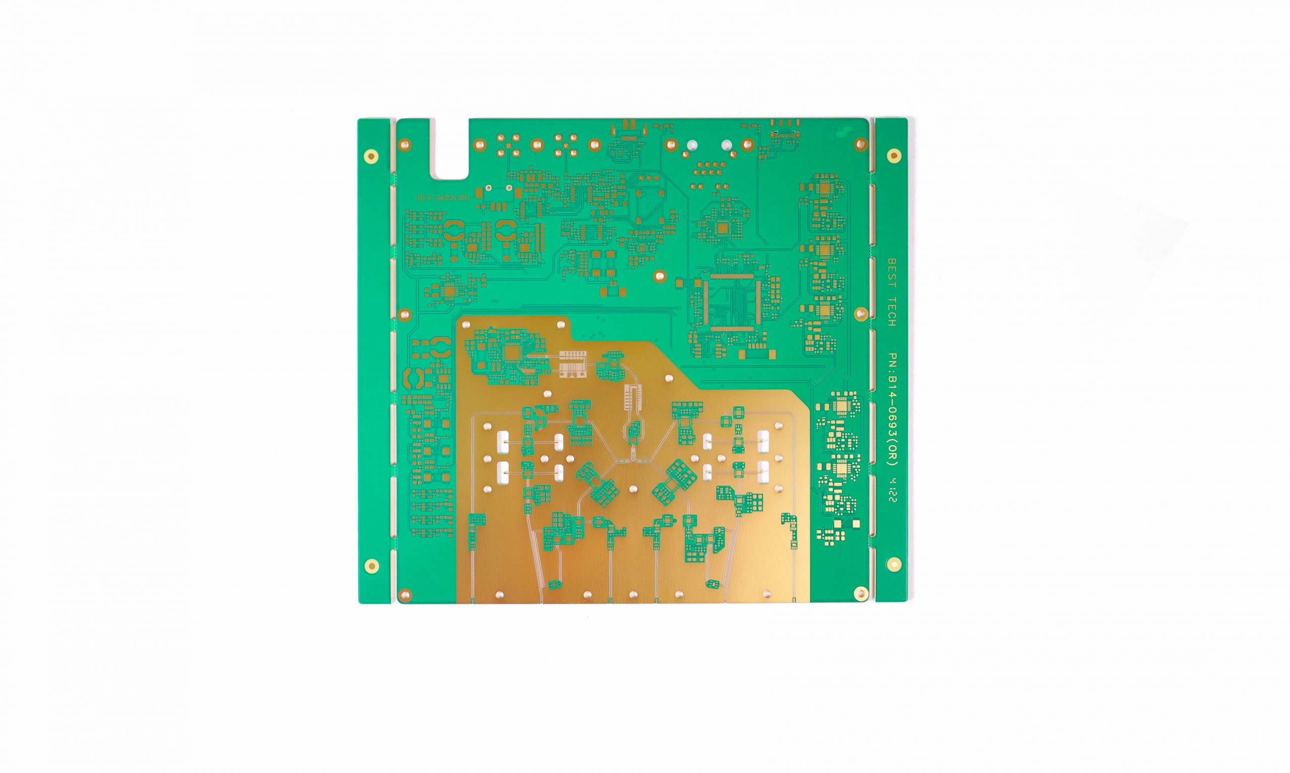
EBest Circuit (Best Technology) excels as a leading one-off PCB manufacturer by delivering industry-leading 24-hour rapid prototyping with a 98.5% on-time delivery rate. Our advanced manufacturing capabilities support complex PCB types including 20+ layer HDI boards, high-speed designs with 112Gbps signal integrity, and high-frequency RF circuits up to 77GHz. With ISO 9001-certified production facilities featuring 5μm line width/spacing tolerance and 100% electrical testing, we maintain a 99.2% first-pass yield rate. We accept single-piece orders with full customization support, having successfully completed over 15,000 unique prototype projects. Our proprietary quick-turn process combines automated DFM analysis (completed within 1 hour) and optimized production workflows to deliver functional boards in 24 hours while maintaining IPC Class 3 standards. Engineers trust our 10+ years of expertise in handling specialized materials like Rogers, Taconic, and Isola for demanding applications. The combination of our technical capabilities, rigorous quality control (including 3D AOI and impedance testing), and unmatched speed makes us the preferred partner for urgent prototyping needs across aerospace, medical, and telecommunications industries. Welcome to contact us: sales@bestpcbs.com.
What Is One Off PCB?
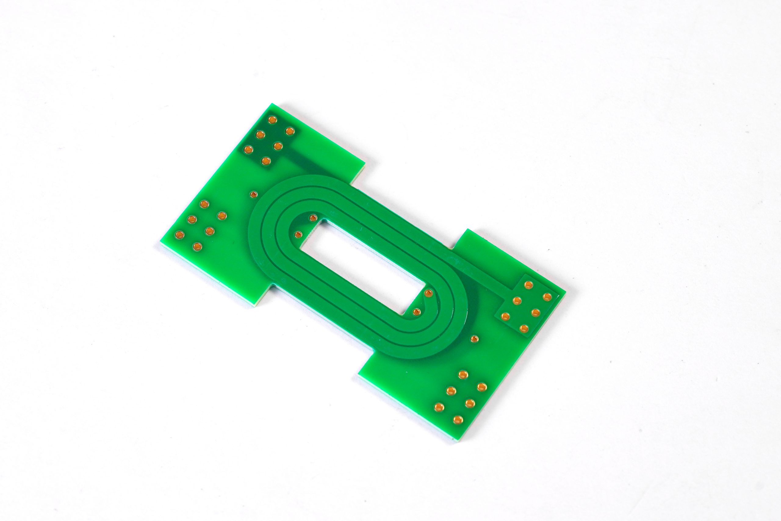
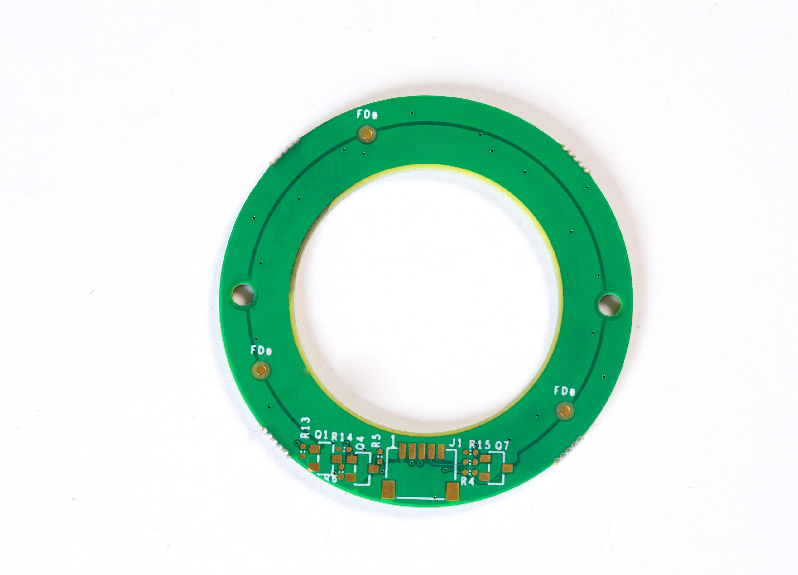
One Off PCB refers to the specialized manufacturing of printed circuit boards in extremely low volumes, typically starting from just a single unit up to small batches. This approach caters specifically to projects needing immediate validation, urgent repairs, or niche applications where mass production isn’t practical. Instead of waiting weeks for conventional orders, engineers can receive fully functional prototypes within 24 hours thanks to streamlined processes like automated design verification and dedicated rapid-turn fabrication lines. These boards support complex requirements including multilayer stacking up to 32 layers, high-frequency materials for RF designs, and precise impedance control, all while eliminating inventory risks and upfront tooling fees. For startups testing innovations or medical labs repairing vital equipment, this model delivers functional electronics at unmatched speed without sacrificing performance. Ultimately, it bridges the gap between conceptual designs and real-world deployment faster than traditional methods.
Why Choose One Off PCB?
Reasons why choose one off PCB:
- Immediate Availability: Unlike traditional PCB production that requires weeks for tooling and processing, One Off PCB delivers functional prototypes or replacement boards within 24 hours. This eliminates project delays when testing new designs or addressing urgent hardware failures.
- No Minimum Order Restrictions: Engineers can order a single unit without committing to large batches. This prevents excess inventory costs and allows iterative testing with multiple design versions before finalizing production.
- Cost-Effective for Prototyping: Small-scale production avoids upfront tooling fees and setup charges typically associated with mass manufacturing. Budgets stay controlled while maintaining access to professional-grade fabrication.
- Supports Complex Technical Needs: From 6-layer HDI boards to RF-optimized designs with impedance control, these services accommodate advanced requirements without compromising quality or precision.
- Reduces Time-to-Market: Startups and R&D teams accelerate product development by receiving physical boards within one business day. Faster iterations mean quicker validation and commercial deployment.
- Flexible Material Selection: Specialized substrates like high-frequency laminates or thermal-conductive materials are available even for single-unit orders, ensuring performance matches end-use conditions.
- Built-In Quality Verification: Automated optical inspection and electrical testing come standard, reducing the risk of receiving non-functional prototypes that could derail project timelines.
- Simplified Logistics: Dedicated rapid-turn production lines prioritize small orders, eliminating the queue delays common in traditional factories focused on bulk manufacturing.
How Does One Off PCBs Solve Urgent Engineering Needs?
Here’s how one off PCBs manufacturing effectively addresses urgent engineering requirements:
- Accelerated Turnaround Times: Standard PCB production cycles take weeks, but One Off services deliver functional boards within 24 hours. This rapid response prevents costly project stalls during critical development phases or equipment failures.
- On-Demand Design Flexibility: Engineers can submit last-minute design revisions without delaying production. Real-time file validation systems ensure manufacturability checks happen within hours, not days.
- Emergency Replacement Solutions: When field equipment fails, manufacturers can receive identical replacement boards overnight. This minimizes operational downtime in industries like medical devices or industrial automation.
- Instant Prototype Validation: Product teams test physical iterations immediately after design adjustments. Continuous hardware verification shortens development cycles by 60-80% compared to traditional methods.
- Scalable Production Ramp-Up: Projects can transition seamlessly from single prototypes to small batches using identical manufacturing parameters. This eliminates requalification delays when moving to volume production.
- Specialized Material Readiness: High-frequency, high-temperature, or flexible substrates remain available for urgent orders. Material databases pre-approve alternatives if primary stocks run low.
- Integrated Testing Protocols: Automated optical inspection and flying probe testing verify board functionality before shipment. Engineers receive working units rather than untested prototypes.
- Global Logistics Networks: Partnered shipping providers guarantee same-day dispatch with customizable routing options. Time-sensitive deliveries reach North American and European destinations within 48 hours.
What Is Process of One Off PCB Manufacturing?
Process of one off PCB manufacturing:
- Design File Submission: Engineers upload standardized fabrication files like Gerber, ODB++, or IPC-2581. Automated systems instantly analyze design integrity and manufacturability.
- Real-Time Engineering Review: Specialized software checks layer alignment, trace spacing, and drill tolerances within minutes. Any inconsistencies trigger immediate designer notifications for rapid corrections.
- Material Preparation: Precision-cut laminates matching specified thickness and dielectric properties advance directly to production. Copper-clad cores stand ready for urgent thermal or high-frequency applications.
- Automated Imaging: Laser direct imaging transfers circuit patterns onto panels with 25-micron precision. Ultra-violet curing solidifies photoresists without traditional phototool delays.
- Rapid Etching: High-pressure chemical etching removes excess copper within controlled environments. Continuous flow systems maintain solution consistency for impedance-critical traces.
- Multilayer Alignment: Hydraulic presses fuse stacked layers under monitored heat and pressure. Registration pins achieve layer-to-layer alignment within ±0.003 inch tolerances.
- High-Speed Drilling: Computer-guided carbide bits create microvias down to 0.15mm diameter. On-machine measurement sensors adjust depth dynamically during operation.
- Surface Finishing: Electroless nickel immersion gold or immersion silver coatings deposit uniformly within 45 minutes. This prevents oxidation while ensuring solderability.
- Solder Mask Application: Inkjet printing deposits epoxy coatings exclusively on designated areas. Near-infrared curing achieves full hardness in under 10 minutes.
- Automated Inspection: Flying probe testers validate electrical continuity across networks. Automated optical scanners detect physical defects at 15-micron resolution.
- Panel Separation: Precision routing machines isolate individual boards without stress fractures. Beveled edges maintain structural integrity for dense component placement.
- Final Validation: Conformity with IPC-A-600 standards confirms solderability, hole wall quality, and surface cleanliness before same-day dispatch.
How to Achieve One Off PCB Manufacture Within 24 Hours?
Below are methods about how to achieve one off PCB manufacture within 24 hours:
- Automated Design Review and Optimization: Advanced software tools instantly analyze uploaded design files, checking for errors and compatibility with production systems. This eliminates manual review delays and ensures issues are flagged and resolved upfront. Clients benefit from faster approval cycles and reduced risk of costly reworks.
- Priority Material Allocation: A curated inventory of frequently used substrates (e.g., FR-4) and finishes (e.g., HASL, ENIG) is maintained for immediate access. By prioritizing in-stock materials, manufacturers avoid supply chain delays, enabling instant production start. Clients save time that would otherwise be spent sourcing custom materials.
- Laser Direct Imaging (LDI) for Precision Etching: LDI technology replaces traditional phototools by etching circuit patterns directly onto the substrate using laser precision. This accelerates the fabrication process while maintaining accuracy. Clients receive high-quality boards with minimal turnaround time.
- Parallel Production Workflows: Multiple processes—such as drilling, plating, and solder mask application—are synchronized to run concurrently rather than sequentially. This optimized scheduling reduces idle time between steps. Clients enjoy shorter overall production timelines without compromising quality.
- Rapid-Cure Surface Finishes: Finishes like ENIG or immersion tin are selected for their quick-curing properties, allowing faster completion of surface treatment. Clients receive boards ready for component assembly sooner, accelerating their product development cycles.
- In-Line Quality Assurance: Automated optical inspection (AOI) and electrical testing are integrated into the production line, not added as post-production steps. This ensures defects are identified and corrected in real time. Clients avoid redelivery delays and gain confidence in the prototype’s functionality.
- Expedited Shipping and Real-Time Tracking: Finished PCBs are packaged and dispatched via priority courier services, with clients receiving instant tracking updates. This transparency helps clients plan their next steps efficiently.
How Does One Off PCB Manufacture Reduce Costs While Ensuring Quality?
Below are the measures about how one off PCB manufacture reduce costs while ensuring quality:
- Standardized Material Selection and Design Templates: By maintaining an inventory of frequently used substrates and finishes, manufacturers avoid premium pricing for custom materials. Additionally, pre-verified design templates streamline the setup process, reducing engineering hours and minimizing errors. Clients save on material costs and design iteration expenses.
- Automated Production Workflows: Laser direct imaging (LDI) and computer-controlled drilling eliminate the need for manual tooling, which is both time-consuming and prone to errors. Automation ensures consistent precision, reducing scrap rates and rework costs. Clients benefit from higher first-pass yields and faster turnaround times.
- Real-Time Quality Monitoring: Integrated automated optical inspection (AOI) systems detect defects during fabrication, not after completion. This proactive approach prevents costly batch rejections and ensures only compliant boards advance to finishing stages. Clients avoid delays and expenses from faulty prototypes.
- Economies of Scale in Procurement: Bulk purchasing of materials like copper-clad laminates and solder masks lowers per-unit costs. Even for small-batch orders, these savings are passed to clients, making premium materials more affordable. This balance between volume discounts and customization benefits project budgets.
- Optimized Supply Chain Logistics: Partnerships with local suppliers reduce lead times for components and finishes. This minimizes inventory holding costs and avoids price volatility from overseas sourcing. Clients gain price stability and faster access to essential materials.
- Rapid Prototyping for Early Validation: Delivering functional prototypes quickly allows clients to test designs in real-world conditions before full-scale production. Identifying issues early prevents expensive modifications later. Clients save on redesign costs and accelerate time-to-market.
- Transparent Cost Modeling Tools: Online calculators provide instant quotes based on design complexity, material choices, and urgency. This empowers clients to adjust parameters (e.g., board thickness or finish type) to meet budget targets without sacrificing essential features. Predictable pricing avoids unexpected surcharges.
How to Test Quality in One Off PCB Production?
Below are specific testing methods about how to test quality in one off PCB production:
- Automated Optical Inspection (AOI): High-resolution cameras scan the board for surface defects such as solder mask misalignment, trace gaps, or excess copper residues. This non-contact method quickly identifies issues like opens, shorts, or incorrect component placements. Clients benefit from faster defect detection compared to manual checks, reducing rework delays and ensuring cosmetic and functional standards are met.
- Flying Probe Electrical Testing: Movable probes contact test points on the PCB to verify electrical connectivity without requiring custom test fixtures. This method checks for opens, shorts, and resistance deviations across all nets. Clients save on fixture costs while gaining confidence in circuit integrity, especially for low-volume or complex designs.
- X-Ray Inspection for Hidden Layers: X-ray systems peer through the board to validate inner-layer connections, via quality, and solder joint integrity in blind or buried vias. This is crucial for multi-layer PCBs where visual access is limited. Clients avoid costly failures caused by internal defects that might escape surface-level checks.
- Thermal Cycle Testing: Boards undergo rapid temperature fluctuations (e.g., -40°C to 125°C) to simulate years of operational stress. This accelerates aging tests, revealing potential failures in material adhesion or component bonds. Clients gain assurance that their prototypes will withstand real-world conditions, reducing field failures and warranty claims.
- Impedance Control Verification: For high-speed designs, time-domain reflectometry (TDR) measures signal integrity by validating impedance continuity across traces. This ensures compliance with specifications like ±10% tolerance. Clients avoid signal integrity issues in applications such as RF or high-speed digital circuits, minimizing performance risks.
- Microsection Analysis: Cross-sectional samples of the PCB are polished and examined under a microscope to assess layer-to-layer adhesion, copper plating thickness, and hole wall quality. This destructive but precise method confirms internal structural integrity. Clients receive documented proof of compliance with industry standards like IPC-6012.
- Functional Circuit Validation: The PCB is powered up and tested under real-world operating conditions using automated test equipment (ATE). This verifies that all subsystems perform as designed, from power regulation to signal processing. Clients identify firmware or hardware conflicts early, accelerating debugging and final product launch.
Can One Off PCBs Handle Complex Designs?
Yes, One Off PCBs can handle complex designs. Modern manufacturing capabilities enable the production of intricate layouts with high precision, ensuring even the most demanding specifications are met. Advanced technologies like laser direct imaging (LDI) and microvia drilling allow for fine-pitch traces, high-density interconnects, and multi-layer configurations. Materials such as high-Tg laminates and controlled impedance substrates support high-frequency or high-power applications. Rigorous testing protocols, including automated optical inspection (AOI), X-ray analysis, and thermal cycling, validate both surface-level and hidden layer integrity. For clients, this means prototypes can mirror final product complexity, enabling thorough validation of signal integrity, thermal performance, and mechanical robustness before scaling to mass production. By leveraging these capabilities, One Off PCB manufacturing reduces the risk of costly design flaws and accelerates time-to-market for sophisticated electronics projects.