PCB manufacturing PCB manufacturing
Home > Blog

Posts Tagged ‘metal clad pcb’

China Metal Clad PCB Manufacturer, Over 19 Years
Tuesday, November 25th, 2025

Why choose China metal clad PCB? This blog is mainly about China metal clad PCB manufacturer list and how to choose a reliable metal core PCB manufacturers in China.

Are you troubled these issues with metal clad PCB?

  • Does your heat dissipation solution consistently hinder overall system performance in high-temperature scenarios?
  • How to address board deformation and lifespan reduction caused by high-power devices?
  • Can traditional substrates simultaneously meet the balance requirements of thermal conductivity and cost control?

As a China metal clad PCB manufacturer, Best Technology can provide you service and solution:

  • Precision Thermal Management Service: Achieve stable heat dissipation performance with a thermal conductivity ≥8W/m·K through customized aluminum/copper substrate layer design.
  • Structural Reinforcement Process: Utilize metal core lamination technology to increase board bending strength by 40%, adapting to the vibration environments of high-power LEDs/automotive electronics.
  • Cost Optimization Solution: Help customers reduce overall material costs by 15% through intelligent matching of conductive layer thickness and standardized production processes.

Welcome to contact us if you have any request for metal clad circuit board: sales@bestpcbs.com.

Why Choose China Metal Clad PCB Manufacturer?

Advantages of China Metal Clad PCB Manufacturer:

  • Significant Cost-Effectiveness and Globally Leading Performance: China boasts a complete electronics manufacturing industry chain and large-scale production capabilities, making its raw material procurement, processing costs, and logistics efficiency highly competitive. The production cost of metal-based PCBs (such as aluminum-based and copper-based PCBs) is 20%-40% lower than in Europe and the United States, with no hidden additional costs, helping customers reduce total product costs and enhance market competitiveness.
  • Highly Mature Supply Chain and Controllable Delivery Cycle: China’s PCB industry clusters (such as the Pearl River Delta and Yangtze River Delta) bring together a complete industry chain from substrate supply and etching to surface treatment, enabling “one-stop” procurement. The delivery cycle for regular metal-based PCB orders is only 7-15 days, and urgent orders can be shortened to 3-5 days, far faster than the international average, meeting customers’ rapid time-to-market needs.
  • Strict Quality Control and Compliance with International Standards: Leading Chinese PCB manufacturers generally hold international quality system certifications such as ISO 9001, IATF 16949 (automotive industry), and UL, and use advanced equipment such as AOI (Automated Optical Inspection) and X-ray inspection to ensure product yield. Key indicators of metal-based PCBs, such as thermal conductivity, withstand voltage, and dimensional accuracy, all comply with EU RoHS and REACH environmental regulations, reducing export compliance risks for customers.
  • Rapid Technological Iteration and Outstanding Customization Capabilities: Chinese manufacturers continuously invest in the R&D of metal-based PCBs, mastering core technologies such as high thermal conductivity material formulations, microvia processing, and precision etching. Customized development of specialized substrates for special applications such as high-power LEDs, automotive electronics, and 5G communications is possible, including ultra-thin aluminum substrates (thickness below 0.3mm) and high-heat-dissipation copper substrates (thermal conductivity > 200W/m·K), meeting diverse customer needs.
  • Leading Environmental Processes and Sustainable Green Manufacturing: Chinese PCB companies actively adopt environmentally friendly processes such as lead-free soldering, water-based inks, and waste gas recovery, reducing carbon emissions and harmful substance emissions during production. Metal substrates have a recyclability rate of up to 95%, meeting the requirements of European and American customers for a circular economy and ESG (Environmental, Social, and Governance) principles, helping customers enhance their brand image.
Why Choose China Metal Clad PCB Manufacturer?

Top China Metal Clad PCB Manufacturers List

Shennan Circuits

  • Business: High-end printed circuit boards, package substrates, electronic assembly.
  • Strengths: Technologically advanced in metal-based PCBs (e.g., power amplifier metal substrates); products certified by multiple industry standards; offers end-to-end services from design to manufacturing. Its “power amplifier metal-based printed circuit boards” are recognized as a manufacturing single-champion product by the Ministry of Industry and Information Technology (MIIT).

Jingwang Electronics

  • Business: Full-range PCB products including rigid, flexible, and metal-based circuit boards.
  • Strengths: One of China’s few platform-type manufacturers covering rigid, flexible, and metal-based PCBs; leading domestic technology in metal-based PCBs (MPCB); integrates upstream metal-based copper-clad laminate resources; achieves higher product gross margins.

Sihui Fushi

  • Business: High-reliability industrial PCBs including metal-based, rigid-flex, and HDI boards.
  • Strengths: Focused on industrial and automotive sectors; products meet international reliability standards; well-regarded in Japanese markets; offers rapid response and customization capabilities.

Xingsen Technology

  • Business: IC package substrates, PCB prototypes, and small-batch boards.
  • Strengths: Deep technical accumulation in semiconductor test boards and package substrates; FC-BGA package substrates in small-batch production; expanding into high-end metal-based PCBs.

Yito Electron

  • Business: High-precision multilayer boards, metal-based PCBs, thick copper boards.
  • Strengths: Long-term supplier to international clients for automotive electronics and telecom equipment; stable quality systems and scalable delivery capabilities.

Best Technology

  • Business: Specializes in metal-based PCBs (aluminum, copper) for LED lighting and power modules.
  • Strengths: Patented technologies in thermal design and high-thermal-conductivity insulation layers; automated production lines with strong cost control.

Zhuoyue Huayu Circuits

  • Business: Research, production, and sales of various metal-based PCBs.
  • Strengths: Supplies high-end LED lighting brands with metal-based PCBs; holds multiple patents; products certified by UL, CE, and other international standards.

How to Choose China Metal Clad PCB Manufacturer?

1. Professional Qualifications and Industry Experience Verification

    • Certification Standard Verification: Prioritize manufacturers with ISO 9001 quality management system certification, UL safety certification, and RoHS environmental certification. These internationally recognized certifications directly reflect the standardization of their production processes and the safety of their products.
    • Industry Focus Assessment: Examine whether the manufacturer focuses on the metal substrate PCB field, rather than simply offering it as an ancillary product line for general PCBs. Check their website’s case study library to see if they have successful project experience in high-heat-dissipation-demand scenarios such as LED lighting, automotive electronics, and high-frequency communications.
    • Technology Patent Reserves: Focus on whether the manufacturer possesses core technology patents in metal substrate material processing, thermal management design, and special surface treatments. This reflects their technological barriers and innovation capabilities.

    2. End-to-End Quality Control System

      • Raw Material Traceability Management: Require manufacturers to provide a supplier list and material testing reports for metal substrates (such as aluminum, copper, and stainless steel) to ensure that parameters such as substrate purity, thickness tolerance, and thermal conductivity meet international standards (such as IPC-4101).
      • Production Process Monitoring: Focus on whether the company uses automated production lines combined with manual quality inspection, particularly its control over key process points such as drilling accuracy, circuit etching uniformity, and solder mask adhesion.
      • Finished Product Testing Standards: Require third-party testing reports, including thermal resistance testing, withstand voltage testing, and salt spray testing, to ensure products meet the mandatory certification requirements of the target market (e.g., EU CE, US FCC).

      3. Supply Chain Response and Delivery Capabilities

        • Capacity Flexibility Assessment: Inquire about minimum order quantity (MOQ), delivery time (e.g., 7-14 days for standard parts, 15-30 days for customized parts), and peak capacity to ensure they match project timelines.
        • Logistics Solutions: Inquire about partnerships with international express companies such as DHL and FedEx, or full container load (FCL) sea freight services, and clarify packaging standards (e.g., moisture-proof and shockproof packaging) and transportation insurance coverage.
        • Inventory Management Transparency: For standard products, request a real-time inventory tracking system; for customized products, confirm the complete timeline from design confirmation to mass production.

        4. Cost-Effectiveness and Pricing Transparency

        • Quotation Structure Breakdown: A detailed quotation is required, including material costs, processing fees, mold fees, testing fees, etc., to avoid hidden charges. Compare quotations from multiple suppliers, but be wary of potentially low-priced quotes that may conceal quality risks.
          • Cost Optimization Suggestions: Reputable manufacturers should provide Design for Manufacturability (DFM) feedback, such as optimizing panel structures to reduce material waste or recommending more economical surface treatment processes (e.g., HASL vs. ENIG).
          • Long-Term Cooperation Agreements: For large-volume orders, tiered pricing or annual framework agreements can be negotiated to secure more favorable prices and priority in resource allocation.

          5. Cross-Cultural Communication and Technical Support

            • Multilingual Service Capability: Confirm that the sales team has English or the target customer’s language communication skills to avoid misunderstandings due to communication barriers.
            • Technical Liaison Team: A dedicated engineer is required for technical liaison, providing value-added services such as thermal simulation analysis and electrical performance optimization, and supporting collaborative processes such as Gerber document review and BOM verification.
            • After-sales service guarantee: Clearly define the warranty period (usually 1-3 years), return and exchange policy, and emergency response time (e.g., 24-hour technical support hotline).
            How to Choose China Metal Clad PCB Manufacturer?

            Why Choose Best Technology as China Metal Clad PCB Manufacturer?

            Reasons Why Choose Us as China Metal Clad PCB Manufacturer:

            • 19+ Years of Expertise in Metal Clad PCB Manufacturing: Deep industry accumulation ensures technical reliability from material selection to final delivery, providing mature solutions for complex designs.
            • Free DFM (Design for Manufacturing) Analysis: Professional pre-production optimization identifies potential process risks early, reduces defects, shortens R&D cycles, and improves first-pass yield.
            • 24-Hour Rapid Prototyping for Urgent Orders: Accelerates product verification and iteration, enabling faster time-to-market and competitive advantage.
            • End-to-End One-Stop Solutions: Integrates design support, manufacturing, and assembly, minimizing cross-process communication costs and enhancing project efficiency.
            • Rigorous Multi-Stage Quality Control System: Full-process control from raw materials to finished products, backed by ISO13485:2016, ISO9001:2015, IATF164949, REACH, and RoHS certifications, ensuring consistency and reliability.
            • Strict Compliance with International Environmental Standards: Lead-free and halogen-free processes meet REACH and RoHS requirements, facilitating global market access and environmental compliance.
            • Competitive Pricing with Guaranteed Quality: Scalable production, lean manufacturing, and optimized supply chains deliver cost efficiency without compromising quality.
            • Dual Certifications for Medical & Automotive Applications: ISO13485 (medical) and IATF164949 (automotive) certifications validate expertise in high-reliability sectors, building trust in product performance.
            • Customized Technical Collaboration & Support: Expert teams provide tailored design advice and process optimization to resolve challenges like thermal management and CTE matching, enhancing final product performance.
            Why Choose Best Technology as China Metal Clad PCB Manufacturer?

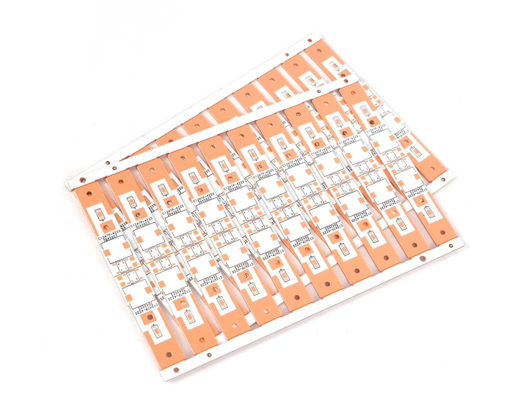
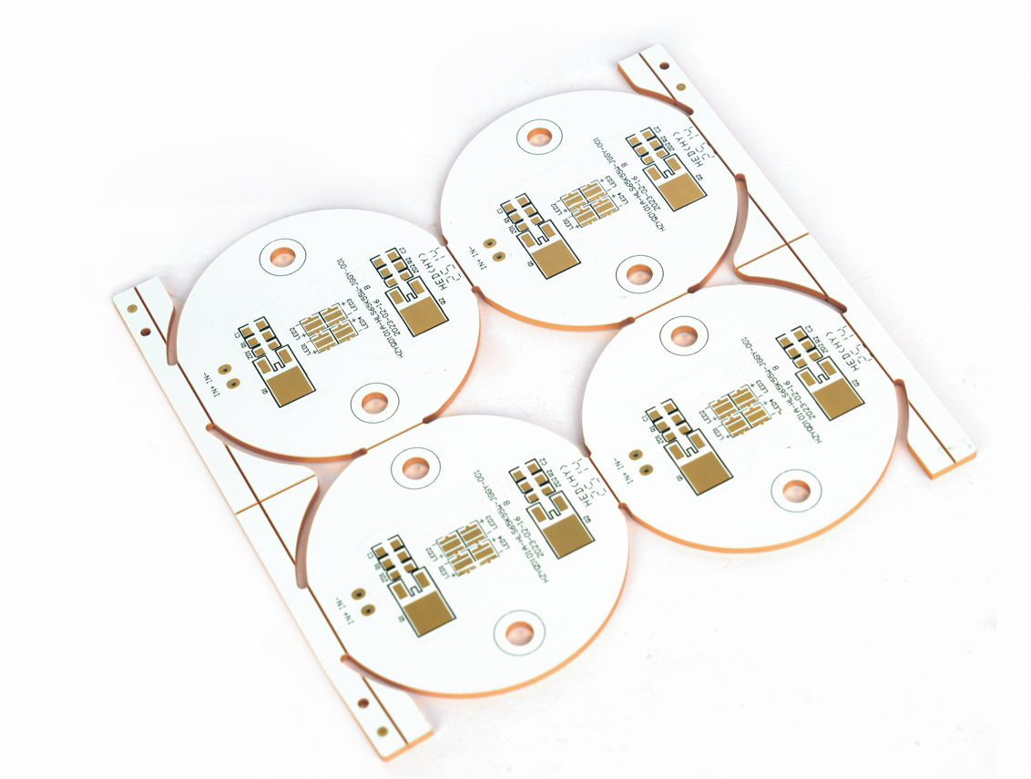
            Our Metal Core PCB Manufacturing Capabilities

            Parameter CategorySpecifications/Range
            Base Material        Aluminum/Copper/Iron Alloy
            Thermal Conductivity (Dielectric Layer)0.8 W/(m·K), 1.0 W/(m·K), 1.5 W/(m·K), 2.0 W/(m·K), 3.0 W/(m·K)
            Board Thickness       0.5mm~3.0mm (0.02″~0.12″)
            Copper Thickness      0.5 OZ, 1.0 OZ, 2.0 OZ, 3.0 OZ, up to 10 OZ
            Outline ProcessingRouting, Punching, V-Cut
            Soldermask ColorWhite/Black/Blue/Green/Red Oil
            Legend/Silkscreen Color       Black/White
            Surface FinishingImmersion Gold, HASL (Hot Air Solder Leveling), OSP (Organic Solderability Preservative)
            Max Panel Size600mm × 500mm (23.62″ × 19.68″)
            Packing Method        Vacuum Packaging/Plastic Bag Sealing
            Sample Lead Time (L/T)           4~6 Days
            Mass Production Lead Time (MP)5~7 Days

            Our Quality Certifications for MCPCB

            • ISO9001:2015
            • ISO13485:2016
            • REACH
            • RoHS
            • IATF16949

            Case Studies of Our Metal Clad PCB Project

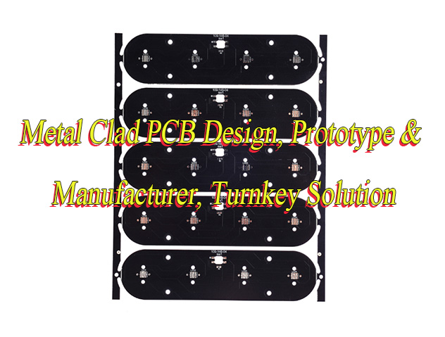
            Case Name: Metal Clad PCB Solution for High-Power LED Street Light Cooling System

            Client Background:

            A European urban lighting equipment manufacturer plans to upgrade traditional high-pressure sodium street lights to high-brightness LED street lights to reduce energy consumption and extend service life. The original design used FR-4 substrate, which caused severe LED chip overheating and significant light degradation during prolonged full-power operation, leading to high maintenance frequency and substandard lifespan.

            Core Issues:

            • LED junction temperature exceeded 105°C, causing approximately 20% reduction in light efficiency;
            • FR-4 substrate insufficient cooling in ambient temperature range of -20°C to 50°C, resulting in street light lifespan of only approximately 20,000 hours;
            • High urban maintenance costs due to frequent lamp replacements.

            Solution:

            Material Selection

            • Aluminum substrate with thermal conductivity of 2.0 W/(m·K) replaces traditional FR-4 (approximately 0.3 W/(m·K));
            • Dielectric layer thickness of 0.1 mm ensures electrical isolation strength >2 kV while maintaining efficient thermal conduction.

            Thermal Design Optimization

            • Dense thermal vias placed beneath LED solder pads rapidly transfer heat from chips to aluminum substrate;
            • Aluminum substrate back directly contacts heat sink housing, forming an integrated cooling path.

            Manufacturing Process

            • High-reflectivity white solder mask applied to enhance light output efficiency;
            • Surface finish with ENIG (Electroless Nickel Immersion Gold) ensures solder joint reliability and environmental durability.

            Implementation Results

            • Thermal Performance Improvement: LED junction temperature reduced to below 85°C, light degradation decreased from 20% to less than 5%;
            • Lifespan Extension: Average street light lifespan increased to 50,000 hours, meeting urban lighting needs for over 10 years;
            • Cost Savings: System energy efficiency improved by approximately 15%, maintenance cycle extended from 2 years to over 7 years, saving approximately 30% in total lifecycle costs.
            Case Studies of Our Metal Clad PCB Project

            How to Get a Quote for Your Metal Clad PCB Project?

            All Documents Required for Metal Clad PCB Quotation:

            • Design File Package: Provide complete Gerber files (including outer/inner layer circuits, solder mask layer, silk screen layer), drilling files (Excellon format), BOM list (precise to component model/package/quantity), and schematics to ensure consistency with physical prototypes.
            • Technical Parameter Specifications: Clarify layer count (e.g., 2-layer/4-layer), board thickness (1.6mm±0.1mm), copper thickness (1oz/2oz), solder mask color (green/black/blue), surface finish (HASL lead-free/ENIG/OSP), trace width/spacing (≥5mil/5mil), hole diameter (starting from 0.2mm), impedance control values (e.g., 50Ω differential pair), and substrate material types (FR-4/aluminum/Rogers high-frequency material).
            • Process & Quality Requirements: Indicate special process needs (blind/buried vias/back drilling), test point locations, solder mask opening dimensions, pad design rules (avoid overlap with vias), environmental standards (RoHS compliance), reliability test items (thermal shock/vibration tests), and certification marks (UL/CE/ESD symbols).
            • Quantity & Logistics: Specify order volume (prototype/batch), lead time (e.g., 10-15 days for rush), packaging methods (antistatic blister box + moisture barrier bag), international shipping methods (air/sea freight), and destination customs documents (invoice/packing list).
            • Structural & Ancillary Information: Submit structural element diagrams (including connector/mounting hole positions), no-routing zones, barcode placement (42×6mm), board edge clearance (≥20mil), silk screen specifications (character height ≥50mil/uniform direction), and special area markings (high-voltage warning symbols/isolation strips).

            Welcome to contact us if you have any request for metal clad printed circuit board: sales@bestpcbs.com.

            Metal Clad PCB Design, Prototype & Manufacturer, Turnkey Solution
            Monday, October 13th, 2025

            How to design a metal clad PCB? Let’s discover metal clad PCB’s spec, stackup, material selection and design guidelines, manufacturing process and lead time together.

            Are you worried about these problems?

            • How to balance thermal efficiency and signal integrity for metal clad PCBs in high-frequency, high-power scenarios?
            • How to accelerate reliability validation for complex metal clad PCB structures while reducing prototyping time and cost?
            • How to avoid the “trilemma” of performance, cost, and scalability when facing customized metal clad PCB demands?

            As a metal clad PCB manufacturer, Best Technology can provide you service and solutions:

            • Rapid Prototyping Channel: 72-hour turnaround with integrated simulation tools for zero-delay design verification.
            • Thermal Solution Library: Standardized thermal modules + customized thermal management for 30%+ efficiency gain without compromising performance.
            • Cost Optimization System: Full-process technical support from material selection to process refinement, achieving 15% cost reduction for customized metal clad PCBs.

            Welcome to contact us if you have request for metal clad PCBs: sales@bestpcbs.com.

            What is Metal Clad PCB?

            Metal Clad PCB (MCPCB), also known as metal-based copper-clad laminate, is a specialized printed circuit board characterized by replacing traditional FR4 fiberglass substrate with a solid metal plate (typically aluminum or copper). Its structure resembles a three-layer sandwich: the bottom layer is a metal heat-dissipation plate, the middle layer is a thin dielectric and thermal conductive layer, and the top layer is a copper foil layer where circuits are patterned and etched. The primary advantage of this design lies in its exceptional thermal conductivity.

            The metal substrate rapidly transfers and dissipates heat generated by high-power components (such as LED chips, power management ICs, and power transistors), effectively preventing thermal-induced component failures. Consequently, MCPCBs are extensively used in high-power, high-heat electronic applications including LED lighting systems, power converters, automotive electronics, and power amplifiers, serving as a critical material for thermal management solutions.

            What is Metal Clad PCB?

            Metal Clad PCB Specifications

            Parameter CategoryAluminum SubstrateCopper Substrate
            Substrate Material6061 Aluminum AlloyC1100 Pure Copper
            Thermal Conductivity1.0-8.0 W/mK2.0-10.0 W/mK
            Dielectric Strength2.5-15 kV2.5-15 kV
            Substrate Thickness0.5-5.0 mm0.3-3.0 mm
            Copper Foil Thickness1-10 oz (35-350μm)1-10 oz (35-350μm)
            Thermal Resistance (Single Layer)0.5-3.0 °C/W0.3-2.0 °C/W
            Maximum Operating Temperature130-150°C150-200°C
            Flame Retardant GradeUL94 V-0UL94 V-0
            Typical ApplicationsLED Lighting/Power ModulesHigh-Frequency Communication/Laser Devices

            Metal Clad PCB Stackup

            Single-layer MCPCB

            • Structure: Copper foil circuit layer → Insulating layer → Metal substrate
            • Applications: Widely used in LED lighting modules (e.g., COB substrates), automotive LED DRLs, and compact motor control units for direct heat dissipation in simple circuits.
            • Advantages: Low manufacturing cost (30-50% cheaper than multilayer boards); metal substrate acts as direct heat sink with thermal resistance 0.5-1.0°C/W; single-sided routing enables manual/automated assembly for small-batch production.

            Double-layer MCPCB

            • Structure: Top-layer copper → Insulating layer → Metal substrate → Bottom-layer copper (signal only)
            • Applications: Suitable for power conversion modules (e.g., switching power supplies), miniature servo drives, and portable devices requiring dual-layer routing in compact spaces.
            • Advantages: Dual-sided routing maximizes space utilization; supports THT/SMT hybrid assembly; shared metal substrate cools both top-layer power devices and bottom-layer components; thermal via design maintains thermal resistance 1.0-2.0°C/W.

            Multilayer MCPCB

            • Structure: Top-signal layer → Insulating layer → Power/ground layer → Insulating layer → Metal substrate
            • Applications: Applied in high-frequency circuits (e.g., 5G filters), medical imaging equipment, and precision instrument control boards needing complex routing and high-performance thermal management.
            • Advantages: Layered design integrates power/signal/ground planes; optimized impedance control (±5% tolerance for 50Ω traces); supports high-speed signaling (e.g., PCIe 4.0) with reduced crosstalk; thermal via arrays achieve ≤0.8°C/W thermal resistance; blind/buried vias enhance routing density.

            How to Choose Metal Clad PCB Material?

            1. Clarify Core Performance Requirements

            • Thermal management priority: High-power devices (e.g., LED chips, IGBT modules) require aluminum substrates (150-220W/m·K) or copper substrates (350-400W/m·K) with thermal conductivity ≥2W/m·K. Low-power scenarios (e.g., 1W LED) optimize cost with aluminum.
            • Electrical performance matching: Copper substrates (low dielectric loss) for high-frequency circuits (5G filters); copper’s high conductivity (≈58MS/m) for RF applications. Avoid aluminum in high-frequency contexts due to lower conductivity.
            • Mechanical strength/weight: Aluminum for lightweight needs (portable devices); copper/stainless steel for high-strength/corrosion-resistant requirements (automotive electronics).

            2. Scenario-Based Material Selection Strategies

              • LED lighting/power modules: Aluminum dominates for cost efficiency; copper for high-power LEDs (e.g., automotive headlights) with thermal resistance ≤0.8°C/W, extending lifespan by 30%.
              • High-frequency/RF circuits: Copper substrates excel in signal integrity with plated-through-hole support; molybdenum (≈138W/m·K) for extreme temperatures (e.g., laser devices).
              • Automotive/industrial: Stainless steel for corrosion resistance; copper for vibration resistance (low CTE); thermal-electric separation copper enhances heat dissipation by 40%.
              • Medical/precision instruments: Molybdenum/copper for precision routing; halogen-free substrates for biocompatibility.

              3. Cost-Process Trade-offs

                • Cost-sensitive: Aluminum ($140-420 per square meter) for mass production; copper costs 30-50% more but reduces long-term thermal maintenance.
                • Process compatibility: Aluminum requires oxidation coatings; copper supports advanced via technologies; molybdenum needs high-temperature sintering.
                • Manufacturing limits: Metal substrates are mostly single-sided; soldering requires preheating to avoid cold joints.

                4. Environmental & Reliability Considerations

                  • Temperature adaptability: Aluminum ≤130°C, copper ≤200°C; molybdenum tolerates >300°C for aerospace/nuclear applications.
                  • Corrosion resistance: Stainless steel for marine environments; aluminum needs protective coatings.
                  • Compliance: RoHS-compliant, lead-free solder; medical devices require ISO 10993 biocompatibility.

                  5. Verification & Optimization Tools

                    • Thermal simulation: ANSYS Icepak/Flotherm models heat distribution, optimizing paths (via placement, heatsink dimensions).
                    • Material testing: Labs verify thermal conductivity, CTE, dielectric constant (ASTM D5470 standard).
                    • Prototyping: Short-lead-time aluminum prototypes (24-hour prototyping services); copper requires thermal conductivity validation.
                    How to Choose Metal Clad PCB Material?

                    Metal Clad PCB Design Guidelines

                    Below is A Detailed Guidelines to Metal Clad PCB Design:

                    1. Requirement Analysis and Preliminary Planning

                    • Clarify application scenarios: Confirm with the client the operating environment (temperature range, vibration level, spatial constraints), electrical performance specifications (current capacity, signal frequency, impedance requirements), and reliability targets (lifecycle, acceptable failure rate).
                    • Define design boundaries: Identify implicit design-impacting factors not explicitly stated by the client (e.g., thermal management priority, cost sensitivity, assembly process compatibility) and document them in a formal design specification.
                    • Preliminary risk assessment: Based on historical case databases, predict typical failure modes of metal-core PCBs (e.g., thermal stress-induced solder joint cracking, dielectric layer aging) and develop initial mitigation strategies.

                    2. Layout Planning and Structural Optimization

                    • Functional zoning principles: Segment regions by signal type (high-speed digital/analog/power) to isolate sensitive circuits from heat sources, ensuring shortest signal paths without cross-interference.
                    • Heat source placement strategy: Concentrate heat-generating components (e.g., power devices) at the center of the metal-core substrate to leverage its high thermal conductivity for uniform heat dissipation and prevent localized overheating.
                    • Mechanical structure adaptation: Design positioning holes, mounting slots, and connector locations per client assembly requirements; evaluate thermal expansion coefficient compatibility between the substrate and enclosure materials to avoid assembly stress concentration.

                    3. Electrical Performance Specialized Design

                    • Impedance control and signal integrity: For high-speed signal lines, precisely calculate and control characteristic impedance (e.g., 50Ω microstrip), employ differential pair routing, and add ground plane isolation to minimize crosstalk.
                    • Power integrity management: Design low-impedance power planes, use decoupling capacitor arrays to suppress power noise, and optimize heat dissipation paths for power devices via the metal-core’s thermal conductivity to reduce thermal-electrical coupling effects.
                    • EMC design: Control electromagnetic radiation and immunity through ground plane segmentation, shielded cavity design, and filter component placement to meet standards (e.g., CISPR, FCC).

                    4. Thermal Management Design Details

                    • Thermal simulation and iterative optimization: Utilize thermal simulation tools (e.g., ANSYS Icepak) to build 3D thermal models, predict steady-state/transient temperature distributions, and iterate to optimize heat dissipation paths (e.g., adding thermal vias, adjusting component spacing).
                    • TIM selection: Choose appropriate thermal interface materials (e.g., pads, grease) based on thermal resistance requirements to ensure good contact and avoid air gaps that increase thermal resistance.
                    • Forced convection cooling: Where space permits, design heat sinks or fan ducts to combine natural and forced convection for enhanced cooling efficiency in high-power scenarios.

                    5. Design for Manufacturing/Testing (DFM/DFT)

                    • Process capability alignment: Confirm metal-core processing capabilities (e.g., minimum hole size, trace/space width, dielectric thickness) with PCB manufacturers to ensure compliance with factory process specifications and avoid manufacturability issues.
                    • Test point planning: Add test pads or probe access points at critical nodes for in-process electrical testing (e.g., ICT, FCT) and post-repair diagnostics to improve yield and maintainability.
                    • Documentation and labeling: Clearly mark layer stack-up, solder mask definitions, component polarity, and generate detailed production files (Gerber, pick-and-place) to minimize production errors.

                    6. Verification & Reliability Testing

                    • Prototype validation: After engineering sample fabrication, perform electrical testing (impedance, signal integrity), thermal testing (IR thermography, thermal cycling), and mechanical testing (vibration, shock).
                    • Accelerated reliability testing: Conduct high-temperature/humidity tests, thermal shock tests, and power cycling tests per industry standards (e.g., JEDEC, AEC-Q) to validate long-term reliability and expose design flaws.

                    7. Design File Export

                    • File Standardization: Generate industry-standard design packages (Gerber, drill files, BOM, assembly drawings) with clear version control (e.g., RS-274X) for compatibility with manufacturers’ systems. Provide 3D models and footprint libraries to support assembly verification.
                    • Parameter Annotation: Clearly annotate metal-core substrate layer structure (copper thickness, dielectric parameters), surface finish processes, and special process requirements (e.g., blind/buried via tolerances).
                    Metal Clad PCB Design Guidelines

                    How to Make Metal Clad PCB?

                    1. Substrate Cutting and Surface Treatment

                    • Cut the metal-core substrate to design dimensions, perform surface cleaning and roughening treatments (e.g., chemical etching or sandblasting) to enhance adhesion between the metal base and insulating layers. Control surface roughness ≤0.3μm to optimize dry film adhesion.

                    2. Inner Layer Circuit Fabrication

                    • Apply dry film → Expose → Develop → Etch (using acidic copper chloride) to form inner layer circuits. Conduct AOI inspection to ensure no breaks/shorts. Perform brown oxidation treatment on copper surfaces to strengthen interlayer bonding.

                    3. Lamination and Bonding

                    • Alternately stack inner layer boards with prepreg (PP) sheets, then vacuum-press at 180℃/40kgf/cm² to form a multi-layer structure. Ensure layer symmetry to prevent thermal stress-induced warping. Cure resin in a vacuum environment to eliminate air bubbles, followed by trimming and edge grinding to achieve dimensional accuracy.

                    4. Drilling and Hole Metallization

                    • Perform CNC drilling (precision ±0.05mm) or laser micro-drilling (for 0.15mm blind/buried holes). Deburr holes and coat carbon layers as electroplating cathodes. Conduct electroless copper plating (0.3-1μm) → electroplating copper (20-25μm) to achieve conductive holes. Verify coating thickness via X-ray fluorescence.

                    5. Outer Layer Circuit Fabrication

                    • Repeat inner layer steps (dry film application, exposure, development, etching) to form outer layer circuits. For metal-core substrates, integrate thermal paths (e.g., thermal vias, heat sinks) leveraging high thermal conductivity.

                    6. Solder Mask and Surface Treatment

                    • Apply liquid photosensitive solder mask ink, then UV-expose and develop to create solder mask layers. Perform surface treatments (e.g., ENIG, HASL, OSP) to enhance solderability and corrosion resistance.

                    7. Thermal Management Design Optimization

                    • Design thermal paths (e.g., increasing thermal via density, adding heat sinks) based on the metal-core substrate’s high thermal conductivity. Use thermal simulation software to optimize heat dissipation efficiency.

                    8. Shaping and Cutting

                    • Use CNC milling or V-Cut to shape the board to design dimensions, ensuring edge smoothness. Clean and dry the boards, with a minimum spacing of 2× board thickness between pieces to prevent adhesion issues.

                    9. Electrical Testing and Quality Inspection

                    • Conduct 100% flying probe testing for continuity, AOI/AXI for pad alignment and inner layer defects, and impedance testing (e.g., 90Ω for USB differential pairs) to ensure signal integrity.

                    10. Packaging and Shipping

                    • Use vacuum anti-static bubble wrap packaging with desiccant and humidity cards. Secure boards in cartons with thick foam and strapping. Label cartons with part numbers, versions, quantities, and origin. Include quality certificates (solderability reports, test records) and packing lists to ensure dry, shockproof, and ESD-safe transportation.
                    How to Make Metal Clad PCB?

                    Why Choose Best Technology as Metal Clad PCB Manufacturer?

                    Reasons why choose us as metal clad PCB manufacturer:

                    • 19 Years of Expertise: Leverages 19 years of PCB manufacturing experience with a defect database and process knowledge base, reducing client trial-and-error costs by 80% and minimizing production flaws.
                    • Multi-Industry Certification Backing: Holds medical-grade ISO 13485, RoHS, and IATF automotive certifications, meeting compliance requirements for high-demand sectors like automotive and healthcare.
                    • Free DFM Design Analysis: Provides complimentary design-for-manufacturing assessments to preempt design risks (e.g., trace/spacing violations), optimize manufacturing efficiency, and reduce post-modification costs—cut client E’s production cycle by 30%.
                    • Price Competitiveness: Delivers industry-leading cost-effective solutions through supply chain optimization and scaled production, reducing client procurement costs by 15-20% (verified by third-party audit) while enabling precise budget control for projects.
                    • Cost-Sensitive Design Support: Tailors low-cost design strategies to specific client needs, achieving cost optimization via material substitution (e.g., 30% reduction with aluminum alternatives) and process simplification, thereby enhancing product market competitiveness.
                    • Rapid Prototyping for Urgent Orders: Offers 24-hour express prototyping services to shorten development cycles, accelerate design validation, and seize market opportunities—successfully advanced client B’s medical device verification by 3 days.
                    • Efficient Delivery Guarantee: Maintains 99.2% on-time delivery rate (Q3 data) through intelligent production scheduling and logistics collaboration, ensuring end-to-end efficiency from production to delivery.
                    • Strict Quality Control & Full Inspection: Implements 100% batch inspection paired with ISO 9001/IATF 16949 certifications, achieving defect rates below 0.05% to ensure consistent product quality.
                    • Rigorous Quality Traceability System: Ensures full process traceability of quality data, complemented by strict quality control procedures, to guarantee batch compliance with international standards like ASTM B25.
                    • Integrated Turnkey Solutions: Streamlines client supply chain management and boosts project efficiency by 40% through end-to-end solutions spanning design consultation, prototyping, and volume production.

                    Our Metal Clad Printed Circuit Board Capabilities

                    Parameter Capabilities
                    Base MaterialAluminum/Copper/Iron Alloy
                    Thermal Conductivity (Dielectric Layer)0.8 W/(m·K), 1.0 W/(m·K), 1.5 W/(m·K), 2.0 W/(m·K), 3.0 W/(m·K)
                    Board Thickness0.5mm~3.0mm (0.02″~0.12″)
                    Copper Thickness0.5 OZ, 1.0 OZ, 2.0 OZ, 3.0 OZ, up to 10 OZ
                    Outline ProcessingRouting, Punching, V-Cut
                    Soldermask ColorWhite/Black/Blue/Green/Red Oil
                    Legend/Silkscreen ColorBlack/White
                    Surface FinishingImmersion Gold, HASL (Hot Air Solder Leveling), OSP (Organic Solderability Preservative)
                    Max Panel Size600mm × 500mm (23.62″ × 19.68″)
                    Packing MethodVacuum Packaging/Plastic Bag Sealing
                    Prototype Lead Time (L/T)4~6 Days
                    Mass Production Lead Time (MP)5~7 Days

                    How to Get a Quote for Metal Clad PCBs Project?

                    Below is a Material List Required for Quotation:

                    • Design Package: Includes Gerber files, drilling files, BOM list, and process cards to ensure full traceability of manufacturing information and provide precise design basis for quotation.
                    • Substrate Material Specifications: Specifies metal substrate type (aluminum/copper), thickness, dielectric material, and thermal conductivity requirements (e.g., 150-220W/m·K for aluminum substrates), directly impacting material costs and thermal performance.
                    • Quantity & Lead Time: Provides order volume, batch delivery schedules, and 99.2% on-time delivery requirements to facilitate production planning and logistics coordination, ensuring efficient delivery.
                    • Special Process Requirements: Specifies thermal via density (e.g., 15-20 vias/cm²), surface finishes (ENIG/OSP), and high-frequency signal routing rules (e.g., 100±10Ω impedance control), which determine production costs and technical feasibility.
                    • Quality Certification Requirements: Specifies standards such as ISO 9001, IATF 16949, or medical-grade RoHS-compliant lead-free certification to ensure industry compliance and avoid post-certification risks.

                    Welcome to contact us if you have any request for metal clad PCBs: sales@bestpcbs.com.

                    The Silent Killer in Your Metal-Clad PCB: Why Adhesive Thickness Dictates Thermal Performance
                    Tuesday, July 22nd, 2025

                    Heat is the invisible enemy of modern electronics. As devices shrink and power densities soar, efficient thermal management becomes non-negotiable. Metal-clad printed circuit boards (MCPCBs), using aluminum or copper bases, are workhorses for heat dissipation in applications like high-power LEDs, motor drives, and power supplies. Yet, a critical but often overlooked factor lurks within their layered structure: the thickness of the dielectric adhesive layer bonding the circuit to the metal base. This seemingly thin film holds immense power over your thermal performance. Let’s dissect why.

                    The Silent Killer in Your Metal-Clad PCB: Why Adhesive Thickness Dictates Thermal Performance

                    The Core Problem: The Adhesive Layer is a Thermal Bottleneck

                    The fundamental reason adhesive thickness matters boils down to physics: Thermal Resistance. Heat generated by components (like LEDs or MOSFETs) must travel through the adhesive layer to reach the highly conductive metal base (substrate), which then spreads and dissipates it into the environment (via heatsinks, convection, etc.).

                    Adhesive materials, even thermally conductive ones (often called Thermal Interface Materials – TIMs), possess thermal conductivity (measured in W/mK) orders of magnitude lower than the copper traces or the aluminum/copper base. For example:

                    • Aluminum: ~200 W/mK
                    • Copper: ~390 W/mK
                    • Typical Thermally Conductive Adhesive: 1.0 – 4.0 W/mK (though some advanced formulations reach 8-10+ W/mK)

                    This adhesive layer is inherently the highest thermal resistance point in the primary heat path from the component junction to the ultimate heat sink.

                    How Thickness Amplifies the Thermal Bottleneck?

                    The thermal resistance (R_th) of the adhesive layer itself is governed by a simple, yet critical formula:

                    R_th_adhesive = L / (k * A)

                    Where:

                    • R_th_adhesive = Thermal Resistance of the adhesive layer (°C/W or K/W)
                    • L = Thickness of the adhesive layer (meters)
                    • k = Thermal Conductivity of the adhesive material (W/mK)
                    • A = Cross-sectional area for heat flow (square meters)

                    This equation reveals the devastating impact of thickness:

                    1. Direct Proportionality (R_th L): Thermal resistance increases linearly with adhesive thickness. Double the thickness, double the thermal resistance. This is the most significant and direct effect. Thicker adhesive creates a longer path for heat to travel through a poorly conducting material, significantly hindering flow.
                      • Consequence: Higher component operating temperatures (Tj), reduced efficiency, accelerated aging (lumen depreciation in LEDs, shorter lifespan), and potential reliability failures.
                    2. Exacerbating Low Conductivity (R_th 1/k): While k is a material property, the impact of a low k is magnified as thickness increases. A poor adhesive (k = 1.0 W/mK) at 100μm thickness creates much higher resistance than a good adhesive (k = 3.0 W/mK) at the same thickness. Making the layer thicker worsens the penalty for using a low-conductivity material. Optimizing both k and L is crucial.
                    3. Increased Interface Resistance: Heat doesn’t flow perfectly across material boundaries. Microscopic imperfections (roughness, voids, poor wetting) at the interfaces between the component/circuit and the adhesive, and between the adhesive and the metal base, create additional “contact resistance.” While primarily dependent on surface quality and pressure, a thicker layer can sometimes make it harder to achieve optimal intimate contact at both interfaces simultaneously, potentially increasing the effective total interface resistance.
                    4. Extended Heat Path: Thickness literally increases the distance heat energy must travel via conduction through the resistive adhesive material before reaching the highly conductive metal substrate. This longer path inherently slows down heat transfer.

                    Optimizing for Superior Thermal Performance

                    Achieving the best possible thermal performance requires a holistic approach targeting adhesive thickness, material properties, and manufacturing quality:

                    1. Minimize Thickness (L): This is priority #1.
                      • Process Control: Implement rigorous process controls during lamination (pressure, temperature, vacuum) to achieve consistent, ultra-thin bond lines. Advanced techniques like controlled-flow adhesives and precise pressure profiling are key.
                      • Material Selection: Choose adhesives specifically formulated for thin application while maintaining dielectric strength and reliability. Some resin systems (e.g., certain epoxies) inherently allow for thinner layers than others.
                      • Target Range: Strive for adhesive layers in the range of 50μm to 100μm (2-4 mils) where possible, balancing thermal performance with manufacturability and dielectric requirements. Going below 50μm requires exceptional process control.
                    2. Maximize Thermal Conductivity (k):
                      • Filler Technology: Thermally conductive adhesives rely on ceramic fillers (Al₂O₃, AlN, BN, SiO₂) within a polymer resin. Higher filler loading increases k but impacts viscosity and processability. Seek formulations with optimal filler type, size distribution, and loading for maximum k.
                      • Advanced Fillers: Consider adhesives using higher-performance (though often more expensive) fillers like Aluminum Nitride (AlN) or Boron Nitride (BN) which offer significantly higher intrinsic conductivity than standard Alumina (Al₂O₃).
                      • Verified Data: Demand certified k values measured using standardized methods (e.g., ASTM D5470), not just vendor claims.
                    3. Optimize Interface Quality:
                      • Surface Preparation: Ensure excellent cleanliness and appropriate surface roughness/treatment on both the circuit side (usually copper) and the metal base side prior to lamination to promote optimal wetting and adhesion.
                      • Void Elimination: Minimize air bubbles/voids trapped within the adhesive or at interfaces. Use vacuum lamination processes and adhesives with good flow characteristics.
                      • Uniformity: Achieve highly uniform adhesive thickness distribution across the entire board area. Localized thick spots are significant thermal bottlenecks.
                    4. Holistic Design & Material Synergy:
                      • Component Placement: Place high-heat-dissipation components directly over areas of the metal base with the best thermal connection (minimal vias/cutouts underneath).
                      • Copper Weight: Use thicker copper layers (e.g., 2oz, 3oz) on the circuit layer to spread heat laterally before it enters the adhesive, reducing the effective thermal gradient across the adhesive.
                      • Metal Base Choice: For extreme applications, consider copper bases (higher k than aluminum) to further reduce the substrate’s spreading resistance once heat finally reaches it.
                    metal core pcb

                    The Designer’s Checklist for Thermal Success:

                    • Specify Adhesive Thickness: Don’t leave it as an afterthought. Define a maximum allowable thickness requirement in your MCPCB specs (e.g., “Adhesive Layer: ≤ 75μm”).
                    • Demand Certified k Value: Require adhesive suppliers or PCB manufacturers to provide reliable thermal conductivity data.
                    • Prioritize Process Capability: Choose a PCB manufacturer with proven expertise and tight process controls for thin, uniform, void-free adhesive layers. Ask about their lamination process, quality control measures (e.g., ultrasonic scanning for voids), and typical thickness consistency.
                    • Consider Total Thermal Resistance (R_th(j-a)): Ultimately, evaluate the entire thermal path from component junction to ambient. While minimizing adhesive R_th is critical, also ensure efficient heat sinking beyond the PCB.

                    Conclusion: Thin is In (for Thermal Performance)

                    In the high-stakes game of thermal management within metal-clad PCBs, the thickness of the dielectric adhesive layer is not a minor detail; it’s a primary performance dictator. Its inherently low thermal conductivity means that even small increases in thickness dramatically raise thermal resistance, directly leading to hotter components and compromised reliability.

                    By understanding the physics (R_th = L / (k * A)), focusing relentlessly on minimizing thickness through advanced materials and precise manufacturing, maximizing thermal conductivity, and ensuring perfect interfaces, engineers can unlock the full heat-spreading potential of their metal substrates. Ignoring the adhesive layer’s thickness is a surefire way to let thermal problems silently undermine your product’s performance and lifespan. Prioritize thinness, prioritize thermal conductivity, prioritize quality – your components will thank you with cooler operation and longer life.