

Looking for LED PCB heatsink solution? Let’s explores its definition, functions, applications, assembly processes, accuracy control, welding defect prevention, and coating consistency techniques for optimal performance.
EBest Circuit (Best Technology) excels as a premium LED PCB heatsink board assembly manufacturer by combining speed, precision, and expert support. We offer 24 hour rapid prototyping and fast-turn production, ensuring urgent projects meet tight deadlines without sacrificing quality. Equipped with fully automated SMT production lines, we guarantee high-precision assembly and rapid response to dynamic customer demands. Our dedicated engineering team provides one-on-one technical support, assisting with design optimization, thermal management solutions, and real-time troubleshooting. By leveraging advanced manufacturing and personalized expertise, we deliver high-performance, reliable LED PCB Heatsink Board Assembly tailored to your exact specifications—faster, smarter, and more efficiently than competitors. Welcome to contact us if you have any request for LED PCB assembly service: sales@bestpcbs.com.
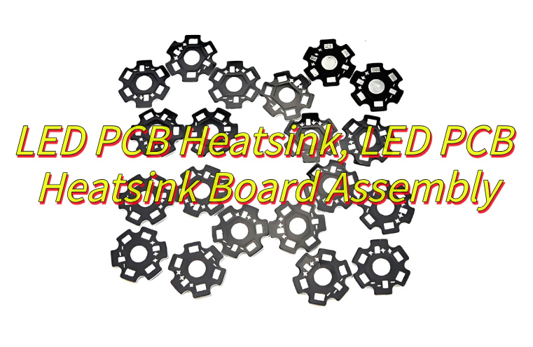
What Is LED PCB Heatsink?
LED PCB heatsink refers to a dedicated thermal management component integrated with light-emitting diode printed circuit boards to dissipate heat generated during operation. This structure typically combines a metal substrate, often aluminum or copper, with a finned or ribbed design to maximize surface area exposure to ambient air. The LED PCB Heatsink acts as a conductive pathway, transferring heat away from sensitive electronic components while maintaining operational stability. Its material selection and geometric configuration directly influence thermal efficiency, with factors like thermal conductivity coefficients and convection coefficients shaping performance. Manufacturers often machine or extrude the LED PCB Heatsink to precise tolerances, ensuring optimal contact with the PCB’s thermal pads. Proper implementation prevents overheating, which could otherwise degrade LED lifespan or cause spectral shifts. By balancing mass, surface area, and aerodynamic profiles, modern LED PCB Heatsink designs address the thermal challenges inherent in high-power lighting applications without adding excessive weight or volume to assemblies.
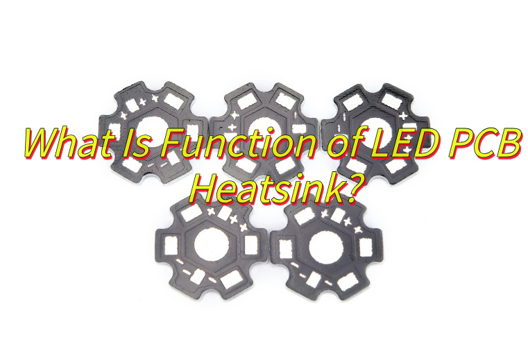
What Is Function of LED PCB Heatsink?
Functions of LED PCB heatsink:
- Thermal Energy Dissipation: The primary role of an LED PCB heatsink is to absorb and distribute heat generated by LED chips during operation. By conducting thermal energy away from sensitive components, it prevents overheating, which could otherwise degrade LED performance or shorten lifespan.
- Operational Temperature Regulation: LED PCB heatsinks maintain stable junction temperatures within safe limits, ensuring consistent light output and color accuracy. This is critical for applications like automotive headlights or studio lighting, where minor temperature fluctuations can cause visible flicker or spectral shifts.
- Enhanced Thermal Conductivity: Materials like aluminum or copper alloys used in heatsinks offer high thermal conductivity, enabling rapid heat transfer from the LED die to the surrounding environment. Finned or pin-array designs further accelerate cooling through convection.
- Structural Stability Support: Beyond thermal management, the heatsink provides mechanical rigidity to the LED PCB, reducing warpage caused by thermal expansion. This is particularly important for multi-layer PCBs in high-power applications like street lighting or industrial fixtures.
- Corrosion and Moisture Resistance: Anodized or coated heatsink surfaces protect against environmental degradation in harsh conditions, such as marine environments or outdoor installations. This extends the service life of both the heatsink and the LED assembly.
- Noise Reduction in Active Cooling Systems: In designs incorporating fans or liquid cooling, the heatsink’s geometry minimizes airflow turbulence, reducing operational noise. This makes it suitable for noise-sensitive applications like residential downlights or theater lighting.
- Compatibility with Advanced LED Packages: Modern heatsinks accommodate surface-mount technology (SMT) LEDs and chip-on-board (COB) arrays through precision-machined mounting interfaces. This ensures efficient thermal coupling even in compact form factors, such as smart bulb modules.
- Recyclability and Sustainability: Aluminum LED PCB heatsinks are fully recyclable, aligning with eco-design principles. Their durability also reduces electronic waste by enabling LED module reuse in retrofit projects or secondary-life applications.
What Are Applications of PCB LED Heatsink?
Applications of PCB LED heatsink:
- Automotive Lighting Systems: LED PCB heatsinks enable high-power LED headlights and daytime running lights to operate reliably in extreme temperatures, ensuring consistent beam patterns and preventing premature failure due to thermal stress.
- Industrial and Commercial LED Fixtures: In warehouses, factories, and retail spaces, heatsinks sustain continuous operation of high-bay lights and track lighting by managing heat buildup, reducing maintenance cycles.
- Consumer Electronics Displays: TVs, monitors, and smartphones utilize miniature heatsinks to cool LED backlight units, preserving image quality and preventing screen discoloration over extended use.
- Architectural and Decorative Lighting: For LED strips, wall washers, and facade lighting, heatsinks maintain aesthetic consistency by preventing color temperature shifts caused by overheating.
- Medical and Surgical Lighting: Operating room lamps rely on heatsinks to stabilize LED output, ensuring surgeons have uninterrupted, shadow-free illumination during procedures.
- Horticultural and Agricultural LED Grow Lights: Heatsinks support 24/7 operation of horticultural LEDs, optimizing heat dissipation to maintain photosynthetic efficiency and extend equipment lifespan.
- Marine and Offshore Lighting: Corrosion-resistant heatsinks enable LED navigation lights and underwater fixtures to withstand saltwater exposure while sustaining performance.
- Aerospace and Aviation Lighting: In aircraft cabin lights and exterior markers, heatsinks ensure LED reliability under extreme altitude-induced temperature fluctuations.
- Entertainment and Stage Lighting: Dynamic LED stage lights and moving heads use heatsinks to prevent overheating during rapid color mixing and gobo projection cycles.
- Smart Home and IoT Devices: Compact heatsinks in smart bulbs and sensors maintain LED efficiency while fitting into space-constrained, thermally challenging environments.

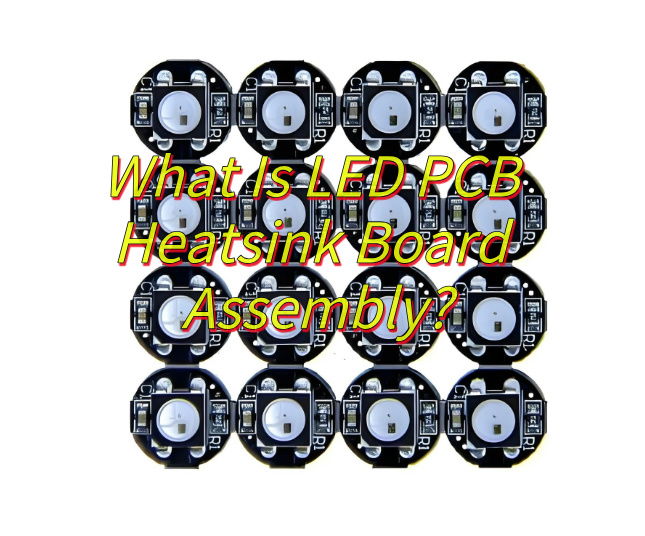
What Is LED PCB Heatsink Board Assembly?
LED PCB heatsink board assembly refers to an integrated thermal management solution combining light-emitting diode components, a metallic substrate, and specialized heat-dissipating structures. This assembly process merges the LED PCB, typically composed of aluminum or copper, with strategically engineered fins, pins, or plates to create a unified system for efficient heat transfer. During fabrication, the LED PCB heatsink board assembly undergoes precise layering of dielectric materials and copper traces to ensure electrical insulation while maintaining thermal conductivity. The design prioritizes maximizing surface area exposure to ambient air or auxiliary cooling systems, enabling rapid dissipation of heat generated by high-power LEDs. Manufacturers often employ machining, stamping, or extrusion techniques to shape the LED PCB heatsink board assembly into configurations tailored for specific form factors, from compact electronic devices to large-scale industrial fixtures. Proper execution of this assembly ensures operational stability, extends LED lifespan, and maintains optical performance by preventing thermal degradation.
What Is Process of LED PCB Heatsink Board Assembly?
Process of LED PCB Heatsink Board Assembly
- Dielectric Layer Application: A thermally conductive dielectric material, such as epoxy resin or ceramic-filled polymer, is coated onto the metallic substrate. This layer ensures electrical insulation between the LED components and the heatsink while maintaining efficient heat transfer.
- Circuit Layer Fabrication: Copper foil is laminated onto the dielectric layer and etched using photolithography or laser ablation to create precise conductive traces. These traces route power and control signals to the LEDs while avoiding thermal hotspots.
- LED Component Mounting: Surface-mount LEDs or chip-on-board (COB) arrays are placed onto the circuit layer using automated pick-and-place machines. Solder paste or electrically conductive adhesive bonds the LEDs to the traces, ensuring both mechanical and electrical connectivity.
- Heatsink Structure Formation: The metallic substrate is machined, extruded, or stamped to form fins, pins, or microchannels. These geometries maximize surface area exposure to ambient air or active cooling systems, enhancing convective heat dissipation.
- Reflow Soldering or Thermal Curing: The assembly passes through a reflow oven to melt solder paste, forming permanent solder joints. For adhesive-bonded LEDs, thermal curing under controlled temperatures activates bonding agents without damaging sensitive components.
- Thermal Interface Material (TIM) Integration: A layer of TIM, such as silicone-based thermal grease or graphite pads, is applied between the LED PCB heatsink board assembly and external cooling modules. This minimizes thermal resistance and ensures efficient heat path continuity.
- Optical and Electrical Testing: Automated systems verify solder joint integrity, LED forward voltage, and light output consistency. Thermal imaging cameras detect hotspots, ensuring the LED PCB heatsink board assembly meets thermal performance targets.
- Final Assembly and Protection: The completed assembly is integrated into lighting fixtures, with secondary optics (e.g., lenses, reflectors) added to shape light distribution. Conformal coatings or potting compounds may be applied for environmental protection in harsh settings.
How to Control the Mounting Accuracy of LED PCB Heatsink Board Assembly?
Process to control mounting accuracy of LED PCB heatsink board assembly:
- Precision Tooling Design
Utilize custom jigs with alignment pins and vacuum chucks to secure the LED PCB heatsink board assembly during assembly. These tools ensure positional repeatability by referencing both the PCB’s edge connectors and the heatsink’s mounting holes, minimizing deviation to ±0.03mm. - Machine Vision Alignment
Deploy high-resolution cameras paired with pattern recognition software to detect fiducial markers on the PCB and heatsink. This system auto-corrects placement angles and offsets, achieving ≤0.01mm alignment accuracy for surface-mount LEDs. - Laser-Based Height Gauging
Integrate spectral confocal displacement sensors to measure the Z-axis clearance between the LED PCB heatsink board assembly and optical components. This ensures planar tolerance of ±0.05mm, critical for beam uniformity in automotive headlights. - Thermal Expansion Mitigation
Conduct finite element analysis (FEA) during design to simulate thermal cycling impacts. Compensate for predicted warpage by optimizing heatsink geometry or using composite materials with matched coefficients of thermal expansion (CTE). - Vacuum-Assisted Reflow Soldering
Employ vacuum reflow ovens with nitrogen inerting to eliminate voids in solder joints. This reduces thermal gradients, maintaining the LED PCB heatsink board assembly’s flatness within 0.02mm across 500mm×500mm panels. - In-Line Coordinate Measurement
Use portable CMM arms with touch-trigger probes to validate critical dimensions (e.g., heatsink fin pitch, LED positional accuracy) at 15-minute intervals. Real-time data adjusts robotic placement parameters to correct drift. - Adhesive Curing with Stress Relief
For bonded assemblies, apply stepwise thermal cycling during curing to pre-release internal stresses. FEA models predict polymer shrinkage, enabling oversized heatsink profiles that shrink to target dimensions post-cure. - Torque-Controlled Fastening
Use servo-electric screwdrivers with angle-monitoring to secure heatsink retention screws. SPC software flags torque deviations exceeding 5%, preventing over-tightening that could distort the LED PCB heatsink board assembly. - Vibration Damping Workstations
Mount assembly stations on active vibration isolation platforms to suppress external disturbances. This maintains placement accuracy for 01005-size LEDs, where positional errors >0.05mm cause luminous flux deviations. - Post-Assembly Laser Interferometry
Perform final validation using dual-frequency laser interferometers to measure surface flatness and parallelism. Corrective actions include lapping heatsink bases or adjusting PCB layer stack-up thicknesses to achieve <0.02mm total indicated runout (TIR). - By implementing these steps, manufacturers ensure the LED PCB heatsink board assembly meets stringent accuracy requirements for applications like medical surgical lights or aviation navigation systems, where micron-level deviations impact performance and safety.
How to Avoid Welding Defects in LED PCB Heatsink Board Assembly?
Measures to avoid welding defects in LED PCB heatsink board assembly:
- Pre-Welding Surface Preparation
Clean the LED PCB heatsink board assembly and component leads using plasma or ultrasonic cleaners to remove oxides, oils, and particulates. Apply flux selectively to high-risk areas (e.g., ground planes) to prevent solder splattering without contaminating optical sensors. - Reflow Profile Optimization
Develop temperature profiles with gradient-controlled heating rates (1–3°C/sec) and soak zones at 150–180°C to activate flux while minimizing thermal shock. Use infrared pyrometers to monitor substrate temperature, avoiding peaks exceeding 245°C for lead-free solders. - Nitrogen Atmosphere Control
Maintain <50ppm oxygen levels in reflow ovens using closed-loop nitrogen injection systems. This reduces solder dross formation by 80% and prevents oxidation of nickel-gold PCB finishes, critical for fine-pitch LED packages. - Stencil Design for Solder Paste Deposition
Employ laser-cut stainless steel stencils with area ratios ≥0.66 and aperture walls tapered at 5–10°. This ensures optimal solder paste release for 0.3mm pitch LEDs, minimizing voids under QFN components. - Solder Paste Inspection (SPI)
Implement 3D SPI systems to verify solder paste volume (±10% target), area, and height pre-reflow. Reject assemblies with volume deviations >15% to prevent tombstoning or solder balling in LED arrays. - Component Placement Force Calibration
Set pick-and-place machine nozzle forces to 2–5N for 0201-size LEDs and 8–12N for larger packages. Over-pressure damages LED epoxy bodies, while under-pressure causes positional shifts during reflow. - Selective Soldering for Thermal Mass Compensation
Use localized soldering nozzles with 4–6mm diameters for through-hole LED leads. Program wave height at 1.5–2mm and contact time <3 seconds to avoid overheating adjacent SMD components on the LED PCB heatsink board assembly. - Void Reduction via Vacuum Assist
Integrate vacuum chambers into reflow ovens to evacuate at 200–220°C, reducing solder joint voids to <10% for large BGA-style LED drivers. This improves thermal cycle reliability by 30%. - Post-Weld Automated Optical Inspection (AOI)
Deploy multi-angle AOI systems with UV lighting to detect lifted leads, solder shorts, and non-wetting on gold-plated heatsink pads. Machine learning algorithms improve defect classification accuracy to >99%. - Destructive Physical Analysis (DPA) Sampling
Conduct microsectioning of 0.1% of assemblies weekly to validate intermetallic compound (IMC) thickness (1–3μm for SnAgCu) and fillet geometry. Adjust reflow profiles based on cross-sectional findings. - ESD Control During Handling
Ground operators via wrist straps (<10^6Ω resistance) and use ionizing blowers at workstations. Static discharge >500V damages LED junctions, causing premature failure in automotive DRL modules. - Rework Station Calibration
Certify hot air rework stations quarterly with NIST-traceable thermocouples to maintain ±5°C accuracy. Overheating during LED replacement degrades adjacent solder joints, creating reliability risks.
How to Maintain the Consistency of Protective Coating in Bulk LED PCB Heatsink Board Assembly?
Measures to maintain consistency of protective coating in bulk LED PCB heatsink board assembly:
- Material Standardization and Batch Tracking
Source conformal coatings from a single supplier with strict viscosity (800–1200 cP) and solids content (30–40%) specifications. Implement a barcode system to track material lot numbers, ensuring no mixing of batches with differing cure rates or chemical compositions. - Automated Spray Coating Systems
Deploy robotic spray booths with electrostatic discharge (ESD) control to apply coatings at 30–50μm thickness. Program nozzle oscillation patterns (±15° swing, 200mm/s traverse speed) to eliminate edge buildup on LED PCB heatsink board assembly edges. - Environmental Chamber Conditioning
Pre-condition assemblies in 23±2°C/50±5%RH chambers for 4 hours pre-coating to stabilize substrate moisture content. Maintain coating/curing environments at 25±1°C/45±3%RH to prevent solvent popping or orange peel defects. - UV Curing with Dose Control
Use mercury-xenon UV lamps with 365nm peak emission and 1–5J/cm² adjustable dosages. Integrate radiometers to verify cumulative exposure, preventing under-curing (tackiness) or over-curing (embrittlement) of acrylic or urethane coatings. - Laser Profilometry for Thickness Verification
Equip inline inspection stations with confocal chromatic sensors to measure coating thickness at 5 points per board. Reject assemblies with deviations >10% from target using pneumatic diverters, maintaining ±3μm uniformity. - Dye Penetrant Inspection for Pinholes
Apply fluorescent dye (0.5% concentration in isopropanol) to cured coatings under UV light. Detect 0.1mm diameter pinholes missed by automated systems, particularly near solder mask edges on the LED PCB heatsink board assembly. - Cross-Hatch Adhesion Testing
Perform ASTM D3359 tests on 0.5% of production batches using 1mm spaced cuts. Require ≥4B adhesion ratings (95% coating retention) across aluminum, copper, and FR4 substrate regions. - Solvent Resistance Validation
Subject coated assemblies to 24-hour immersion in isopropyl alcohol (70% concentration). Measure contact angle changes (>10° deviation triggers process audit) to detect incomplete curing or coating degradation. - Thermal Cycle Exposure
Run 100-cycle (-40°C to +125°C) tests on 0.2% of production lots. Monitor coating cracking via edge-glow inspection under UV light, with <0.2mm crack length acceptable per IEC 60068-2-14 standards. - Operator Certification Programs
Train coating technicians on spray gun maintenance (nozzle cleaning every 2 hours) and static charge grounding procedures. Require biannual recertification with hands-on coating quality assessments. - Supplier Quality Agreements (SQA)
Audit coating suppliers quarterly for particle size distribution (D50: 5–15μm) and shelf-life compliance. Reject lots exceeding 6-month storage at 5–25°C to prevent filler sedimentation. - Process Window Analysis
Conduct design of experiments (DoE) to establish robust coating parameters (e.g., 15–25psi atomization pressure, 6–8-inch standoff distance). Publish control charts with ±2σ limits for real-time process monitoring.
By enforcing these controls, manufacturers achieve <0.5% coating-related failure rates in LED PCB heatsink board assemblies, ensuring compliance with MIL-I-46058C and IPC-CC-830B standards while maintaining 15+ year outdoor durability.