Looking for High Thermal Conductivity MCPCB for LED Street Light? Choose EBest First for Premium Quality & Stable Performance
When selecting High Thermal Conductivity MCPCB for LED Street Light, core parameters directly determine the reliability and lifespan of your LED street lighting. EBest’s products are tailored to solve thermal management pain points in LED street lights, with industry-leading specifications.
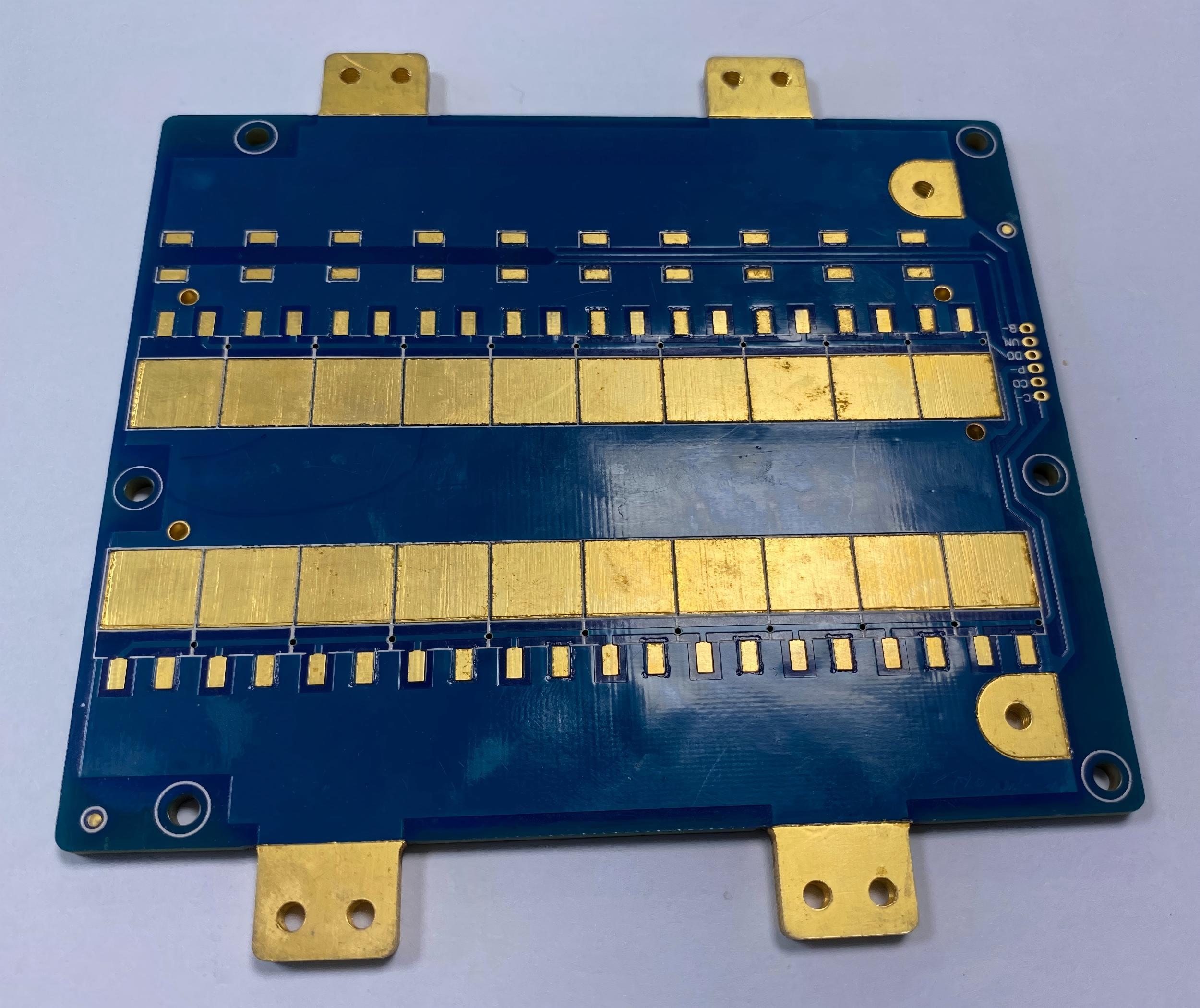
Our High Thermal Conductivity MCPCB for LED Street Light features: Thermal conductivity ranging from 2.0W/(m·K) to 12W/(m·K), 6061-T6 aluminum alloy base, 50-100μm nano-ceramic dielectric layer, 2-4oz electrolytic copper foil, and operating temperature range of -40℃ to 125℃.
All products pass strict thermal cycle and insulation tests, ensuring stable performance in harsh outdoor environments. For your LED street light projects, choose EBest’s High Thermal Conductivity MCPCB—contact us to place your order today.
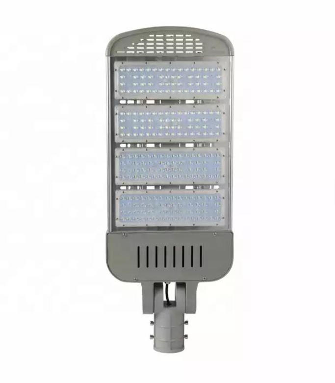
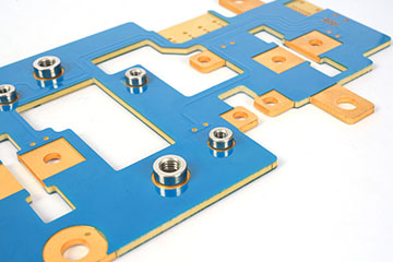
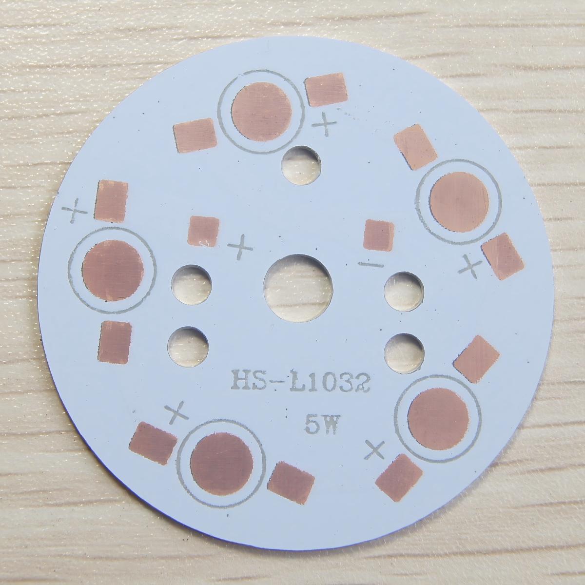
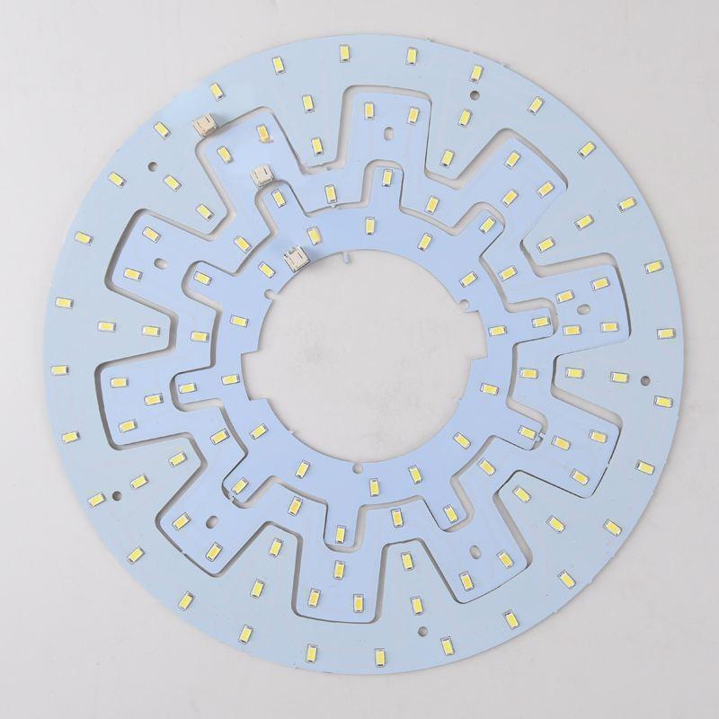
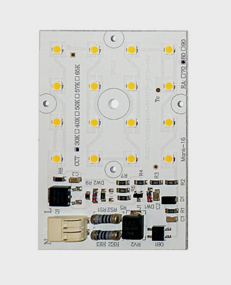
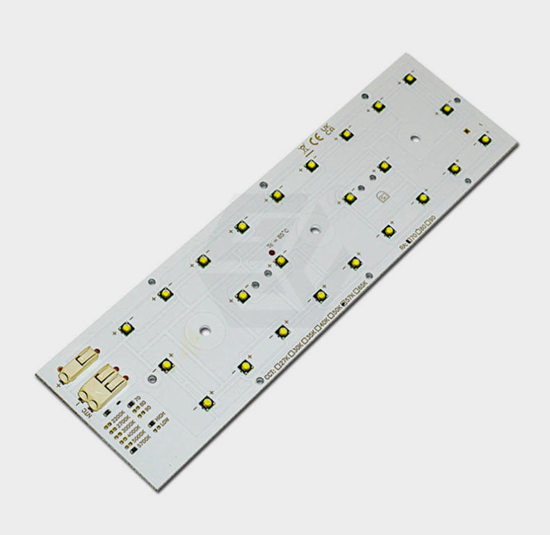
MCPCB for LED Street Light
Why Choose EBest for High Thermal Conductivity MCPCB for LED Street Light?
Quality Assurance: We adopt automatic vacuum lamination and AOI detection, achieving a production yield of over 98.5%. All products comply with international standards and undergo rigorous reliability testing.
Fast Delivery: Our vertically integrated supply chain enables small-batch delivery in 7 days and mass production in 15–20 days, eliminating delays in your project timeline.
Stable Supply Chain: Long-term partnerships with top material suppliers ensure a steady supply of core raw materials, avoiding production interruptions caused by material shortages.
Professional Service: Our technical team provides one-on-one DFM (Design for Manufacturability) advice, optimizing designs for manufacturability and solving technical issues throughout the project cycle.
What Are the Core Pain Points of High Thermal Conductivity MCPCB for LED Street Light, and How Does EBest Solve Them?
Many users face challenges such as poor thermal dissipation, inconsistent production quality, and supply chain risks when using High Thermal Conductivity MCPCB for LED Street Light. EBest addresses these pain points with targeted solutions.
Pain Point 1: Overheating leads to LED light degradation and shortened lifespan. Solution: Our MCPCB uses high-quality thermally conductive dielectric layers, reducing thermal resistance to ≤5℃/W and keeping the LED junction temperature below 85℃.
Pain Point 2: Inconsistent batch production affects product reliability. Solution: We implement strict SPC (Statistical Process Control) and 100% AOI detection to ensure consistent quality across all batches.
Pain Point 3: Long delivery times delay project schedules. Solution: Our in-house production lines and optimized supply chain reduce delivery times by 30% compared to industry averages.
Pain Point 4: Poor insulation performance poses safety hazards. Solution: All our MCPCBs pass 25KV insulation withstand voltage tests, meeting outdoor safety standards. Choose EBest to solve all your High Thermal Conductivity MCPCB for LED Street Light pain points.
What Is High Thermal Conductivity MCPCB for LED Street Light, and Why Is It Essential?
High Thermal Conductivity MCPCB for LED Street Light is a specialized metal-core PCB designed for outdoor LED street lighting, consisting of a metal base, thermally conductive dielectric layer, and copper circuit layer.
LED street lights convert only 20–30% of electrical energy into light, with 70% or more converted into heat. Traditional FR-4 PCBs (with a thermal conductivity of 0.3–0.5W/(m·K)) cannot dissipate heat efficiently, leading to rapid light degradation.
High thermal conductivity MCPCBs solve this issue by transferring heat quickly from LED chips to heat sinks, extending the LED lifespan to over 50,000 hours and ensuring stable brightness.
How to Choose the Right Thermal Conductivity for High Thermal Conductivity MCPCB for LED Street Light?
How to Choose the Right Thermal Conductivity for High Thermal Conductivity MCPCB for LED Street Light?
The right thermal conductivity depends on your LED street light’s power and operating environment. For most municipal street lights (30–50W), 2.0–4.0W/(m·K) MCPCBs are sufficient.
For high-power street lights (50–100W) or areas with high ambient temperatures, choose 4.0–8.0W/(m·K) products. For extreme outdoor environments, 8.0–12.0W/(m·K) high-grade MCPCBs are recommended.
EBest’s technical team can help you select the optimal thermal conductivity based on your specific project requirements, ensuring both cost-effectiveness and performance.
What Are the Key Materials for High Thermal Conductivity MCPCB for LED Street Light?
The performance of High Thermal Conductivity MCPCB for LED Street Light depends on three core materials: the metal base, dielectric layer, and copper foil.
Metal Base
We use 6061-T6 aluminum alloy (with a thermal conductivity of ≥200W/(m·K)) for most projects, balancing thermal performance and cost. For high-end applications, copper or copper-molybdenum alloy bases are available.
Dielectric Layer
Nano-ceramic dielectric layers (50–100μm) are used, offering high thermal conductivity and insulation. They reduce thermal resistance while ensuring electrical safety.
Copper Foil
2–4oz electrolytic copper foil is standard, supporting high current and reducing voltage drop. Heavy copper (4oz+) is available for high-power LED street lights.
How Does High Thermal Conductivity MCPCB Improve LED Street Light Lifespan?
It is an industry consensus that for every 10℃ increase in LED junction temperature, the lifespan decreases by 50%. High Thermal Conductivity MCPCB for LED Street Light directly reduces the junction temperature, significantly extending the lifespan.
Our MCPCB reduces thermal resistance by 40% compared to traditional FR-4 PCBs. In practical tests, LED street lights using our MCPCB maintained 95% light flux after 6,000 hours of continuous operation.
This not only reduces maintenance costs but also enhances the reliability of your LED street lighting projects.
What Are the Top 4 Industry Applications of High Thermal Conductivity MCPCB for LED Street Light?
High Thermal Conductivity MCPCB for LED Street Light is widely used in outdoor lighting and related fields. Below are four popular industry applications with real-world cases.
1. Municipal Road Lighting
Case: Singapore HDB street light project. Our 2.0W/(m·K) MCPCB was used, achieving 98.7% uptime and reducing maintenance frequency by 60%.
2. Highway Lighting
Case: European highway lighting project. High-power (80W) LED street lights used our 6.0W/(m·K) MCPCB, maintaining stable performance in environments ranging from -20℃ to 35℃.
3. Industrial Park Lighting
Case: American industrial park project. Our MCPCB solved overheating issues in high-humidity environments, ensuring a service life of 50,000+ hours.
4. Residential Community Lighting
Case: Asian residential community project. A cost-effective 3.0W/(m·K) MCPCB was used, balancing performance and budget, with 96% customer satisfaction.
How to Compare High Thermal Conductivity MCPCB for LED Street Light with Traditional FR-4 PCBs?
The following table clearly compares High Thermal Conductivity MCPCB for LED Street Light with traditional FR-4 PCBs, helping you make informed decisions.
|
Comparison Item |
High Thermal Conductivity MCPCB for LED Street Light |
Traditional FR-4 PCB |
|
Thermal Conductivity |
2.0–12.0W/(m·K), 4–24 times higher |
0.3–0.5W/(m·K), low |
|
LED Junction Temperature |
≤85℃, safe range |
≥125℃, prone to overheating |
|
LED Lifespan |
50,000+ hours |
20,000–30,000 hours |
|
Outdoor Adaptability |
Resistant to high/low temperatures and humidity; no deformation |
Prone to deformation; poor insulation in harsh environments |
|
Light Flux Maintenance |
95% after 6,000 hours |
82% after 6,000 hours |
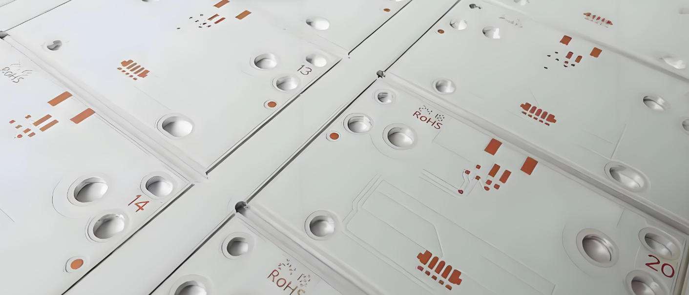
What Are the Production Processes of High Thermal Conductivity MCPCB for LED Street Light?
Stable production processes ensure consistent quality of High Thermal Conductivity MCPCB for LED Street Light. EBest adopts advanced processes to meet high standards.
- Material Cutting: Precision cutting of the metal base and copper foil, ensuring dimensional accuracy of ±0.1mm.
- Dielectric Layer Lamination: Automatic vacuum lamination at 180℃ and 8MPa pressure, eliminating interlayer bubbles.
- Circuit Etching: Precision etching with a line width accuracy of ≥0.2mm, ensuring signal integrity.
- Surface Treatment: Anodization + nano-hydrophobic coating, enhancing corrosion resistance for outdoor use.
- Quality Testing: 100% AOI detection + thermal conductivity testing + insulation testing, ensuring no defective products leave the factory.
What Certifications and Services Does EBest Offer for High Thermal Conductivity MCPCB for LED Street Light?
EBest holds multiple international certifications, ensuring our High Thermal Conductivity MCPCB for LED Street Light meets global quality standards. Our services cover the entire project cycle.
EBest Certifications
|
Certification Name |
Certification Scope |
Validity |
|
UL 796 |
Electrical safety, flame resistance, thermal endurance |
2024–2027 |
|
ISO 9001 |
Quality management system (design to delivery) |
2023–2026 |
|
IPC-A-610 Class 3 |
High-reliability PCB acceptability |
Permanent |
|
IEC 60068-2-1 |
Environmental testing (high/low temperature) |
2024–2027 |
|
RoHS |
Environmental protection (lead-free, cadmium-free) |
Permanent |
EBest Core Services
- DFM Design Advice: Free one-on-one optimization for design for manufacturability (DFM).
- Sample Service: Fast sample production (3–5 days) for performance testing.
- After-Sales Support: 24/7 technical support and problem-solving.
- Full Traceability: Barcode management for complete production process tracking.
Why Is Thermal Management Critical for High Thermal Conductivity MCPCB for LED Street Light?
Poor thermal management of High Thermal Conductivity MCPCB for LED Street Light leads to multiple issues that impact project success.
Overheating causes LED chips to age faster, leading to light degradation, color drift, and premature failure. This increases maintenance costs and damages brand reputation.
Effective thermal management via high-quality MCPCB ensures stable LED performance, reduces downtime, and maximizes your return on investment.
How to Optimize the Design of High Thermal Conductivity MCPCB for LED Street Light?
Optimizing the design improves the performance and manufacturability of High Thermal Conductivity MCPCB for LED Street Light. Follow these key tips.
Thermal Via Design
Add thermal via arrays (8–12 per cm²) under LED chips to transfer heat directly to the metal base, reducing thermal resistance.
Copper Foil Layout
Use wider copper traces for high-current areas to reduce voltage drop and local overheating.
Dielectric Layer Thickness
Choose 50–100μm dielectric layers—thicker layers reduce thermal conductivity, while thinner layers compromise insulation.
Heat Sink Integration
Design the MCPCB to fit seamlessly with heat sinks, ensuring tight contact for efficient heat transfer.
FAQ: Common Questions About High Thermal Conductivity MCPCB for LED Street Light
Below are the most common questions about High Thermal Conductivity MCPCB for LED Street Light, with direct, concise answers.
1. What is the maximum thermal conductivity of EBest’s High Thermal Conductivity MCPCB for LED Street Light?
The maximum thermal conductivity of our High Thermal Conductivity MCPCB for LED Street Light is 12W/(m·K), suitable for high-power LED street lights (100W+).
2. Can High Thermal Conductivity MCPCB for LED Street Light withstand outdoor harsh environments?
Yes. Our MCPCBs have an operating temperature range of -40℃ to 125℃, are waterproof, dustproof, and corrosion-resistant, making them ideal for outdoor use.
3. How long does it take to deliver High Thermal Conductivity MCPCB for LED Street Light in mass production?
Mass production delivery takes 15–20 days. For urgent projects, we offer expedited service with delivery in 10–12 days.
4. Does EBest provide custom High Thermal Conductivity MCPCB for LED Street Light?
Yes. We provide fully customized solutions, including thermal conductivity, size, copper thickness, and surface treatment, tailored to your project needs.
5. How to test the thermal performance of High Thermal Conductivity MCPCB for LED Street Light?
We use professional equipment to test thermal conductivity, thermal resistance, and junction temperature. We also provide test reports for your verification.
6. Are EBest’s High Thermal Conductivity MCPCB for LED Street Light lead-free?
Yes. All our MCPCBs comply with RoHS standards, are lead-free and cadmium-free, and meet global environmental requirements.
7. Can High Thermal Conductivity MCPCB for LED Street Light reduce LED light decay?
Yes. By reducing the LED junction temperature to ≤85℃, our MCPCB slows down light degradation, ensuring 95% light flux maintenance after 6,000 hours.
What Are the Latest Technical Innovations in High Thermal Conductivity MCPCB for LED Street Light?
The industry is constantly innovating, and EBest keeps pace with the latest trends to enhance the performance of High Thermal Conductivity MCPCB for LED Street Light.
Innovation 1: Nano-ceramic dielectric layer with improved thermal conductivity, reducing thermal resistance by 15% compared to traditional dielectric layers.
Innovation 2: Copper-molybdenum alloy base, balancing thermal conductivity and thermal expansion coefficient to reduce warping risk.
Innovation 3: Integrated heat pipe design, further improving heat dissipation efficiency for high-power LED street lights.
Choose EBest for High Thermal Conductivity MCPCB for LED Street Light – Your Trusted Partner
EBest specializes in High Thermal Conductivity MCPCB for LED Street Light, with 19 years of industry experience, strict quality control, and professional technical support.
We provide high-performance, reliable products that solve your thermal management and supply chain challenges. Whether you need standard or custom MCPCBs, we have you covered.
We provide High Thermal Conductivity MCPCB for LED Street Light products. If you have any needs, please place your order with us. Our email is sales@bestpcbs.com. EBest – your reliable partner for LED street light MCPCB solutions.