PCB manufacturing PCB manufacturing
Home > Blog

Posts Tagged ‘ipc 610’

IPC 610 Certification​: Class I vs. Class II vs. Class III
Thursday, August 7th, 2025

If you’re working in electronics manufacturing or sourcing PCB assembly services, you’ve likely come across the term IPC 610. This standard, also known as IPC-A-610, plays a major role in ensuring the quality and reliability of electronic assemblies. Whether you’re dealing with consumer gadgets or mission-critical aerospace systems, understanding IPC-A-610 can help you make better decisions and achieve higher quality outcomes.

Let’s explore what IPC-A-610 is all about, how it classifies assemblies, and why choosing a PCB manufacturer certified with IPC-A-610 can make a real difference.

What is IPC-A-610 Standard?

IPC-A-610 is a globally recognized standard for the acceptability of electronic assemblies, developed by the IPC. It sets the inspection criteria for electronic assemblies, particularly focusing on how solder joints and components should appear on the finished board.

This standard acts as a visual guide for manufacturers, inspectors, and engineers to determine whether a PCB assembly meets quality expectations. It defines what’s acceptable and what’s not, ensuring that defects are minimized and performance isn’t compromised. The most recent version is IPC-A-610H, though previous versions like IPC-A-610F and IPC-A-610G are still in use in some industries.

IPC 610 Certification

What Are the Classes in IPC-A-610?

IPC-A-610 breaks down its quality requirements into three distinct classes. These classes define the level of workmanship needed based on the end-use of the product.

  • Class I – General Electronic Products
  • Class II – Dedicated Service Electronic Products
  • Class III – High-Performance Electronic Products

IPC-A-610 Class I vs Class II vs Class III

1. Class I – General Electronic Products

Class I represents the basic level of acceptability for electronic assemblies. Products in this category are designed for simple, everyday use, where the main concern is that the device works—not how it looks or how long it lasts.

Key Features of Class I:

  • Function over form: As long as the product performs its basic function, it’s considered acceptable—even if it has minor cosmetic defects.
  • Loosest inspection standards: Imperfections like uneven solder or slight misalignment may be allowed if they don’t impact performance.
  • Minimal cost and time: Because of the relaxed standards, Class I products are faster and cheaper to manufacture.

Typical Applications:

  • Toys
  • Flashlights
  • Basic household gadgets
  • Low-cost consumer electronics

2. Class II – Dedicated Service Electronic Products

Class II is the most commonly used class in electronics manufacturing. It sets moderate quality standards suitable for products that require reliable performance over time, but where minor cosmetic issues are acceptable.

Key Features of Class II:

  • Performance and lifespan: Devices are expected to work reliably under normal conditions for their intended lifespan.
  • Stricter inspection than Class I: Components must be correctly placed, and solder joints must be solid, though slight cosmetic flaws may still be allowed.
  • Balance of quality and cost: This class strikes a practical balance between reliability and manufacturing efficiency.

Typical Applications:

  • Industrial control systems
  • Consumer electronics (TVs, laptops, phones)
  • Automotive electronics (non-safety critical systems)
  • Networking devices (routers, modems)

3. Class III – High-Performance Electronic Products

Class III is for products that require the highest level of quality and reliability. These are mission-critical applications where even a minor defect could lead to system failure, safety risks, or major financial loss.

Key Features of Class III:

  • No room for error: Every solder joint, component placement, and surface must meet strict inspection criteria with no cosmetic imperfections allowed.
  • Extended reliability and lifespan: Products must perform flawlessly in harsh environments, under continuous use or critical conditions.
  • Higher cost and longer production: The level of detail and inspection required increases both time and production cost.

Typical Applications:

  • Medical devices (life-support systems, diagnostic equipment)
  • Military electronics (communication systems, radar)
  • Aerospace electronics (navigation, avionics)
  • Automotive safety systems (airbags, braking systems)

What Are Common PCB Defects Covered by IPC-A-610?

IPC-A-610 outlines many types of assembly defects, helping manufacturers inspect and correct issues before products reach customers. Some of the most common defects it covers include:

  • Cold solder joints – Dull, grainy joints that may lead to poor electrical contact.
  • Insufficient solder – Joints that don’t provide full coverage, risking weak connections.
  • Solder bridging – Excess solder creating unwanted connections between pads or leads.
  • Component misalignment – Parts not properly placed on pads, affecting function or reliability.
  • Contamination – Presence of dust, oils, or residue that could impact signal integrity or cause corrosion.
  • Lifted pads or traces – Damage to the PCB surface, which can break electrical paths.

Here are some commone defects that can be acceptted by IPC 610 Class I & Class II:
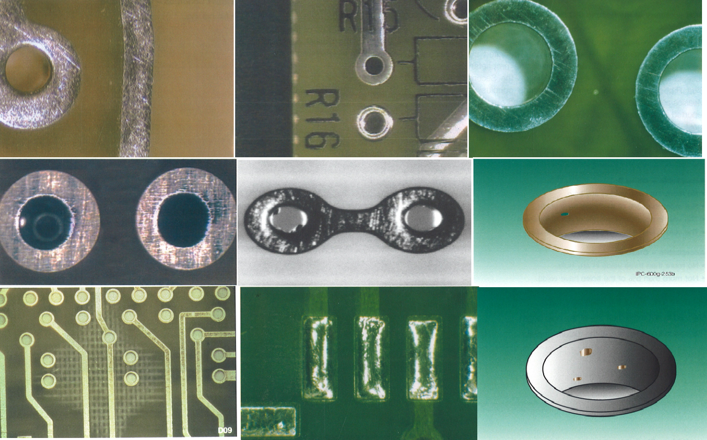
What Are Common PCB Defects Covered by IPC-A-610?

What is the Difference Between IPC-A-610 and IPC J-STD-001?

Many people confuse IPC-A-610 with another widely used standard — IPC J-STD-001. While they are related, they serve different purposes.

  • IPC-A-610 focuses on how the finished assembly should look. It is a visual inspection standard used to judge whether the product is acceptable.
  • IPC J-STD-001 sets the soldering process requirements. It guides manufacturers on how to achieve quality solder joints, covering materials, equipment, and techniques.

In short:

  • J-STD-001 = Process and workmanship standard
  • IPC-A-610 = Visual acceptance standard

Many manufacturers follow both standards together to ensure not only that the product looks correct but also that it was built using reliable processes.

One-Stop PCB Assembly Manufacturer Certified with IPC-A-610

When you need reliable PCB assembly, it pays to choose a manufacturer certified with IPC-A-610. At Best Technology, we follow strict IPC-A-610 Class II and Class III guidelines across our production lines.

Here’s what sets us apart:

  • Certified Inspectors and Assemblers

All staff involved in production and inspection are IPC-A-610 certified, ensuring every board meets required standards.

  • Full Traceability

We use MES (Manufacturing Execution System) to track every step, from incoming materials to final inspection. This guarantees complete traceability and quality control.

  • Serving Demanding Industries

Our IPC-compliant services are trusted in automotive, medical, industrial, and aerospace sectors.

  • Competitive Pricing and Fast Turnaround

With advanced equipment and a professional engineering team, we provide fast, affordable, and reliable PCB assembly services.

Whether you need small-batch prototypes or large-volume production, Best Technology ensures your PCBs meet IPC-A-610 standards, giving you peace of mind with every shipment.

BGA Chipping Per IPC-610: Everything You Need to Know
Friday, September 20th, 2024

What is a BGA chip?

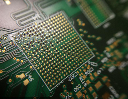
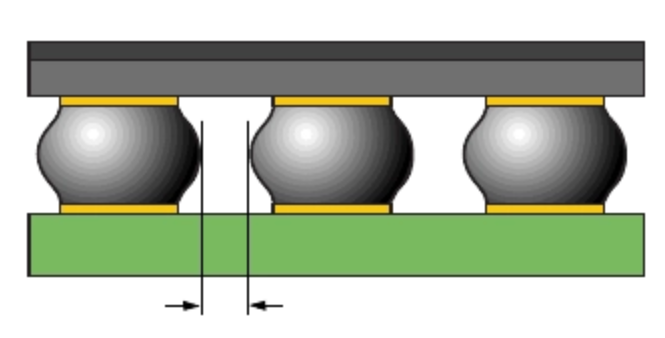
The Ball Grid Array (BGA) is actually a kind of package mode, not the chip itself. BGA is a surface adhesion technology that used in the packaging of integrated circuits, which is interconnected with the printed circuit board (PCB) by making an array solder ball at the bottom of the chip as the I/O end of the circuit. This packaging technology allows the bottom surface of the entire device to be used as a pin, with a shorter average wire length than the surrounding defined package type, resulting in better high-speed performance. BGA package technology is improved from pin grid arrays to provide more pins than other package types such as dual in-line or four-side pin flat packages. Soldering BGA-packaged devices requires precise control and is usually done by automated plant equipment. The BGA package device is not suitable for slot fixing, but is fixed to the PCB by surface mount. BGA packaging technology comes in many forms, including plastic BGA (PBGA), ceramic BGA (CBGA), and others, each of which varies in size, amount of I/O, physical structure, and packaging materials.

BGA Chipping Per IPC-610

BGA chips are popular because of their compact size and ability to provide higher density connections. This allows manufacturers to pack more functionality into smaller devices. It is widely used in electronics to mount microprocessors, memory chips and other components onto printed circuit boards (PCBS), which are then installed into our electronic devices. Such as our smartphones, laptops and advanced electronic devices.

Why is BGA used?

BGA packaging is used primarily due to its ability to offer higher connection density and better electrical performance compared to traditional packages like QFP (Quad Flat Package). The design of BGAs minimizes issues like short circuits and signal interference, which are more common with older pin-based methods. Another reason BGAs are preferred is their superior thermal dissipation capabilities. The solder balls act as conductors, helping to transfer heat away from the chip. Below you can see some other benefits of using BGA chips.

1. High-density package: BGA package can provide a large number of I/O (input/output) connection points in a relatively small space.

2. Miniaturization: The BGA package allows the chip to be mounted directly on the PCB (printed circuit board), reducing the thickness and volume of the package.

3. Good heat dissipation performance: BGA package can better heat dissipation due to its large underside contact area.

4. Reliable electrical performance: BGA package adopts spherical solder joints, which can reduce signal transmission delay.

5. Easy assembly: While the number of I/O pins in the BGA package increases, the pin spacing remains unchanged or even increases, which helps to improve the yield of assembly. 6. Cost effectiveness: Although the initial investment of BGA packaging is high, it can reduce costs in the long run due to its high efficiency and miniaturization capability.

7. Wide range of applications: BGA packages are suitable for various types of integrated circuits from simple microcontrollers to complex graphics processors.

8. Easy maintenance: In some cases, BGA-packaged chips can be replaced or repaired, but this usually requires professional equipment and technology.

9. Mature technology: BGA packaging technology has been very mature, there are many types to choose from, such as PBGA (plastic ball grid array), CBGA (ceramic ball grid array), etc., to meet the needs of different applications.

What does a BGA do?

A BGA plays a crucial role in establishing electrical connections between an IC and the PCB. The tiny solder balls act as both conductors and connectors, allowing signals to flow between the chip and the board. This is critical in enabling the functionality of various devices, from computers to consumer electronics.

Additionally, BGAs enhance the durability and performance of circuits by providing a stable connection that can withstand environmental stress, such as temperature fluctuations or mechanical vibrations. This makes them a preferred choice in mission-critical applications, including aerospace, automotive, and medical electronics.

What is the difference between BGA and flip chip?

The primary difference between a BGA and a flip chip lies in how the chip is mounted onto the PCB. In a BGA, the chip is placed on top of the solder balls, which serve as the connection points between the IC and the PCB. The solder balls are positioned in a grid pattern under the chip. The chip remains on the top surface, with the balls acting as connectors below.

In contrast, a flip chip is mounted upside down, or “flipped.” The connections are made directly between the IC and the PCB, eliminating the need for solder balls. This method makes the active component of the chip face the substrate and can be directly in contact with the substrate, thus improving the thermal and electrical performance. The main advantages of flip chips include high density, which can reduce the size of the package so that more chips can be installed in a limited space. In addition, flip chip technology also has excellent electrical and thermal performance, which can provide better signal transmission and heat dissipation effects. However, it can be more expensive and complex to manufacture, making BGAs a more cost-effective solution in many cases.

BGA chipping per IPC-610

IPC-610, a globally recognized standard for PCB assembly and acceptance, provides guidelines on acceptable levels of chipping in BGAs. According to IPC-610, minor chipping on non-critical areas of a BGA is allowed as long as it does not affect the functionality or reliability of the component.

Section 10.6 of the IPC-610 standard is specific to BGA chips and defines what are acceptable and unacceptable defects. Under this standard, buyers ensure that BGA used in electronic products meets high quality standards and does not compromise the integrity of the finished product. Manufacturers must adhere to these standards to maintain the reliability and safety of their products, especially in industries such as aerospace and medical devices, where component failures can have serious consequences.

The description of BGA in IPC-A-610 standard mainly focuses on the acceptance standards of BGA components, which involve the appearance, structure, and welding quality of BGA components. Specifically, IPC-A-610 standard acceptance of BGA components includes but is not limited to the following points:

  • Appearance inspection

The appearance of BGA components should meet the requirements of the standard, no obvious defects such as cracks, deformation, etc.

  • Welding quality

The welding of BGA components should be uniform and complete, without bad phenomena such as virtual welding and cold welding. The solder joint should be firm and able to withstand certain mechanical stress.

  • Pin/ball grid array inspection

The pin or ball grid array of the BGA component should be well docked with the PCB pad, without dislocation, offset and other phenomena. The pin or ball should be intact and free of defects.

  • Size and position accuracy

The BGA component should be accurately installed on the PCB, and its position and height should meet the design requirements to ensure the normal connection of the circuit and the functional realization of the component.

In addition, as technology evolves, the IPC-A-610 standard is constantly updated to accommodate new technologies and component types. For example, the IPC-A-610G version includes new SMT terminal types and updated plating hole filling requirements, as well as BGA void requirements.

How long does IPC-610 last?

IPC-610 is regularly updated to reflect changes in technology and industry practices. However, the certification itself typically lasts for two years. After this period, manufacturers and technicians may need to undergo recertification to ensure they are up to date with the latest standards and guidelines. The two-year validity helps maintain a high level of competence and ensures that those involved in the production and inspection of PCBs follow the most current best practices.

Recertification is crucial, as it ensures that professionals stay informed about any changes in the IPC-610 standard, particularly regarding evolving technologies like BGAs and their use in modern electronics. This ongoing education helps manufacturers produce high-quality, reliable products that meet the demands of today’s fast-paced tech industry.

What is Section 10.6 of the IPC-A-610?

Section 10.6 of the IPC-A-610 standard provides specific criteria for the inspection and acceptance of BGA chipping. It outlines the types of chipping that are considered acceptable and those that are not. Minor cosmetic chips on the non-functional areas of a BGA are usually acceptable as long as they do not interfere with the operation or reliability of the chip. However, chipping on functional areas, such as those that could affect the solder ball connections, is not allowed.

What is the difference between IPC-600 and IPC-610?

IPC inspection standards refer to the inspection of electronic components according to IPC-A-600 and IPC-A-610 standards. IPC-A-600 is an inspection standard for printed circuit boards (PCBs), while IPC-A-610 is an inspection standard for electronic assembly. These two standards are the most commonly used inspection standards in the electronic manufacturing industry, which specify the appearance, size, welding quality and other requirements of electronic components.

First, the IPC-A-600 standard specifies the appearance and size requirements of the printed circuit board. According to the standard, the printed circuit board should be free of any surface defects, such as bubbles, cracks, scratches, etc. In addition, the size of the printed circuit board should meet the design requirements, the aperture, line width, line distance and other parameters must also meet the standard provisions. Only printed circuit boards that meet these requirements can be considered qualified.

Second, the IPC-A-610 standard specifies the inspection requirements for electronic assembly. According to this standard, welding quality is one of the most important inspection contents in electronic assembly. The welding should be uniform and firm, and the welding point should have no defects such as virtual welding, dislocation, short circuit and so on. In addition to the welding quality, the installation position, direction and spacing of the components also need to meet the standards. Only electronic assemblies that meet these requirements can be considered qualified.

When carrying out IPC inspection, it is necessary to carry out inspection and evaluation in strict accordance with the requirements of the standard. First of all, it is necessary to accurately understand and master the content of IPC-A-600 and IPC-A-610 standards, and understand the requirements and testing methods therein. Secondly, appropriate inspection equipment and tools should be used, such as microscopes, calipers, welding quality detectors, etc., to ensure the accuracy and reliability of the inspection. Finally, it is necessary to accurately record and evaluate the inspection results, timely discover and correct unqualified products, and ensure quality control in the production process.

With over 18 years as an industry leader, Best Technology is one of the most experienced PCB and PCB assembly manufacturer in Asia. We are highly specialized not only in quick-turn PCB prototype and PCB assembly, but also medium and small volume PCB fabrication. In Best Technology, you can enjoy a full-comprehensive one-stop service from PCB design, layout, PCB fabricate, PCB assembly, function testing and delivery. We always try our best to fabricate your PCB with copper clad laminate with the highest quality to meet your demands.
If you have any questions, please feel free to contact us with sales@bestpcbs.com, we will be happy to help you.

What is IPC standard for PCB?
Monday, June 28th, 2021

Do you know what is IPC standard for PCB?IPC, it is a trade association whose goal is to standardize the assembly and production requirements of electronic devices and components.  It was established in 1957 as the Institute of Printed Circuits.  IPC has developed thousands of standards and specifications to regulate the electronics manufacturing industry.

IPC standards are related to PCB design, production technology, electronic assembly, etc., in order to achieve high reliability, high quality, high performance, and meet user specifications.

What are the IPC Standards for?

Before we can understand IPC standards, we first need to know who made them. It comes from the IPC Association, a trade association whose goal is to standardize assembly and production requirements for electronic devices and components. It was founded in 1957 as the Printed Circuit Research Institute. Its name was later changed to the Institute for Electronic Circuit Interconnection and Packaging to highlight the expansion from bare boards to packages and electronic components. In 1999, the organization officially changed its name to IPC with the slogan “Association Connecting Electronics Industries”.

What is IPC standard for PCB?

IPC standards are the most widely recognized code of acceptability in the electronics industry. The organization publishes standards for nearly every stage of the electronic product development cycle, including design, procurement, assembly, packaging, and more. In other words, IPC standards refer to everything in the electronics industry and are the basic knowledge of designers and manufacturers.

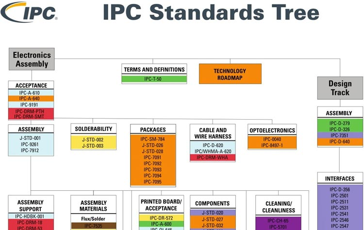
Just like the IPC standards tree, there are many different aspects of standards that all serve the end product. IPC-A-610, for example, focuses on the acceptability of electronic components and is used worldwide by original equipment manufacturers and EMS companies.

What is the PCB IPC Standard?

IPC plays a vital role in the PCB industry by establishing standards that cover every stage of PCB production from design to manufacturing. These standards ensure consistency and compatibility throughout the PCB process. During the design phase, IPC standards guide file formats, PCB design software, design guidelines, and electronic product documentation. They also affect the material selection of PCB components, surface mount equipment and surface treatments. In addition, these standards are essential for testing and evaluating the acceptability of printed boards.

When it comes to welding, IPC standards cover a variety of techniques, including reflow soldering, wave soldering and welding. These guidelines help companies determine whether their electrical and electronic components meet quality expectations during manufacturing. IPC standards also address cable and harness assemblies to ensure they meet standards.

The most widely recognized IPC standard for PCBs is IPC-6011, which Outlines the performance requirements for PCBS. However, IPC-6012 is more specific and governs the qualification and performance of rigid PCBs. IPC-6012 covers everything from how the PCB should be made to its thickness and the integrity of the copper layer. Compliance with this standard ensures that PCBs meet electrical and mechanical performance expectations. Whether you’re creating boards for high-end computers or small consumer devices, compliance with PCB IPC standards is critical to meeting industry and customer expectations. Here is the IPC tree for your reference:

What is IPC standard for PCB?

What is the IPC Level of PCB?

One of the most widely used industry standards in the manufacturing of printed circuit boards is IPC-A-610C Acceptability of Electronic Assemblies and IPC-A-600 Acceptability of Printed Boards. This standard is used primarily for the incoming inspection of bare boards from a PCB fabricator.

In the IPC-A-610C document, electronic products are divided into level 1, level 2, and level 3. The higher the level, the stricter the quality inspection conditions. Here are how 3 levels divided:

Level 1 products: called general-purpose electronic products. Including consumer electronic products, certain computers and their peripherals, and products whose main purpose is to use functions.

Level 2 products: called dedicated service electronic products. Including communication equipment, complex industrial and commercial equipment and high-performance, long-life measuring instruments. Under normal use environment, this kind of product should not malfunction.

Level 3 products: called high-performance electronic products. Including high-reliability, long-life military and civilian equipment that can continue to operate. This kind of product must not allow any interruption failure during use, and at the same time, it is necessary to ensure the reliable startup and operation of the equipment in a harsh environment. Such as medical life-saving equipment and all military equipment systems.

For PCB manufacturing, do you know which IPC standards are commonly used?

What is IPC standard for PCB?
multilayer pcb

IPC Standard for PCBs

The IPC has created several standards for printed circuit board (PCB) design, manufacturing, and assembly. Here I would like to share you some standards which we mainly use:

  • IPC-2221

A general standard that covers almost every aspect of PCB design, including electrical considerations, thermal design, and manufacturing-ready design.

  • IPC-2222

A guide for rigid PCB cross-sectional design, including recommendations for board thickness, hole aspect ratio, and dielectric clearance.

  • IPC-2223

A standard for reliable Flex-PCB design, including guidelines for material selection, impedance control, and pad placement.

  • IPC-2224

A standard for PC card form PCBs, including design requirements for organic and inorganic materials, and single, double, or multilayered interconnections.

  • IPC-A-610

A standard for PCB assembly that classifies PCBs into three quality levels, with Class 1 being the lowest and Class 3 being the highest.

  • IPC-6011

General Performance Specification for Printed Boards

  • IPC-6012

Appraisal performance and specifications for Rigid printed boards

  • IPC-6013

Appraisal performance and specifications for Flexible printed boards

  • IPC-6016

Fixed performance and specification of HDI or printed circuit board of high density interconnection layer

  • IPC-SM-840

Appraisal and performance of permanent performance

  • IPC-HM-860

Multilayer Hybrid Circuit Specification

  • J-STD-003

Solderable test for printed boards

  • IPC-A-600F

Acceptance conditions for printed boards

  • IPC-4761

Design Guide for Protection of Printed Board Via Structure

What is IPC standard for PCB?
resin filled production bpm20599

What is IPC-A-610 Standard?

IPC-A-610 Standard is one of the most widely recognized standards in the electronics industry, specifically focusing on the acceptability of electronic assemblies. It provides detailed guidelines and criteria for the inspection of PCB assemblies, so that these assemblies meet the necessary quality levels for their intended use. Its main content includes:

1. Soldering Criteria

IPC-A-610 provides in-depth guidelines on acceptable soldering techniques, covering solder joints, surface mount devices (SMDs), through-hole components, and wire terminations. It explains what constitutes an acceptable versus defective solder joint, ensuring that the electrical connections are reliable.

2. Component Placement

The standard includes criteria for the correct placement and alignment of electronic components on PCBs. It specifies the acceptable tolerances for misalignment and ensures components are correctly placed for proper electrical performance and physical integrity.

3. PCB Assembly Defects

IPC-A-610 details different types of assembly defects, such as insufficient solder, tombstoning, lifted pads, and more. Each defect is categorized based on its severity and impact on the function and reliability of the product, providing guidance on whether a defect can be accepted or if it requires rework.

4. Classes of Electronic Assemblies

The standard divides electronic assemblies into three classes based on the end-use of the product:

  • Class 1 – General electronic products
  • Class 2 – Dedicated service electronic products
  • Class 3 – High-performance products

5. Mechanical Assembly

IPC-A-610 provides criteria for the mechanical aspects of PCB assemblies, such as mounting hardware, screws, connectors, and wire routing.

6. Coating and Potting

The standard covers the application of protective coatings (conformal coatings) and potting materials that protect the PCB from environmental damage such as moisture, dust, or chemicals. It specifies acceptable thicknesses, coverage areas, and inspection methods.

7. Cleaning Requirements

The cleanliness of PCB assemblies is critical for preventing performance degradation over time. IPC-A-610 outlines acceptable levels of residues from fluxes and other contaminants and specifies methods for inspecting and verifying cleanliness.

8. Cable and Wire Harness Assemblies

The standard includes requirements for assembling and inspecting cable and wire harnesses.

9. Solderless Wire Wraps

The standard also touches on solderless wire-wrapped connections, which are used in some applications where soldering is not practical or preferred. IPC-A-610 defines the acceptable criteria for such connections.

10. Inspection and Testing

    The IPC-A-610 standard provides guidelines for visual inspection and testing methods used to evaluate whether an assembly meets the required acceptability criteria. This can include both automated and manual inspection processes, depending on the class of product.

    Why IPC Standard is Important?

    IPC standards are of great importance to the circuit board industry.

    1. IPC standard specifies the requirements for all aspects of the design, manufacturing and assembly of the circuit board, including material selection, size specifications, welding quality, reliability testing, etc., providing a unified reference and guide for circuit board manufacturers to improve product quality and reliability.

    2. IPC standards can help communicate and cooperate between PCB manufacturers and customers. By referring to IPC standards, the two parties can reach a consensus on PCB specifications, quality requirements and other aspects, reduce misunderstandings and disputes, and improve production efficiency.

    3. For customers, IPC standards provide confidence. When a company adheres to these standards, they can trust that the final product will be reliable and durable, even in demanding environments.

    4. In addition, IPC standards also contribute to the technological innovation and development of the circuit board manufacturing industry. By being in line with international standards and understanding the latest technological trends and standard requirements, manufacturers can continuously improve production processes and equipment, improve production efficiency and product quality, and enhance competitiveness.

    At the same time, IPC regularly updates and revises standards to meet changing technology and market needs.

    What is the IPC Standard for PCB Clearance?

    PCB clearance, or the distance between conductive components, is essential to avoid electrical shorts or interference. Without proper clearance, electrical shorts could occur, potentially leading to device failure or safety hazards. The IPC-2221 standard covers PCB design and provides guidelines for this clearance, ensuring safety and functionality. This standard specifies how much space is needed between traces, pads, and other conductive materials depending on the operating voltage. However, the minimum clearance between any two conductors on a PCB depends on the device’s intended use and voltage: 

    • General-purpose devices: 0.1 mm (4 mils) 
    • Power conversion devices: 0.13 mm (5.1 mils) 
    • Class 2 and 3 PCBs: 0.25 mm (10 mils) for low voltage and 0.5 mm (20 mils) for high voltage 
    What is IPC standard for PCB?

    What are the IPC Standards for PCB Repair?

    PCB repair can be tricky, but IPC-7711/7721 offers guidance on how to properly rework and repair PCBs. These standards provide detailed procedures for everything from removing defective components to repairing damaged traces and soldering issues.

    By following IPC-7711/7721, technicians can restore a PCB to its original condition without compromising its performance. This is critical in industries where PCBs are expensive or difficult to replace, such as aerospace and medical devices. Repair standards also reduce the environmental impact by extending the life of the PCB, making repairs more sustainable.

    It is no problem for us to manufacture the PCB following the standard in IPC 6012 /6013 Class 2 and Class 3, as well as following to the standard listed above. These acceptance conditions are the basis for the inspection of our company’s products, as well as the working standards of the employees at the production site, and also become an important part of the training of the employees for PCB production and assembly in our company.

    Send us your PCB drawing, let’s help to make your PCB design into a real board.