

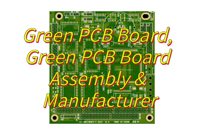
Seeking for green PCB board solutions? Dive into materials, assembly tips, manufacturer selection, and color advantages, including blue PCB comparisons—for reliable, fast-delivery boards with <10% BGA voiding.
What Is Green PCB Board?
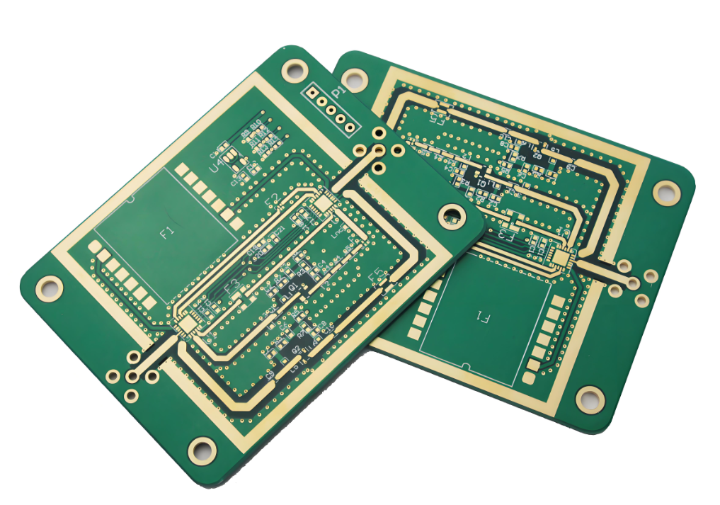
A green PCB board refers to a printed circuit board (PCB) coated with a green solder mask, primarily composed of epoxy-based resin that cures into a distinctive green hue for enhanced circuit protection and optical functionality. This green PCB board offers superior advantages in manufacturing, including reduced eye strain during manual inspections, optimized visibility in TTL rooms for AOI calibration, and cost-efficiency due to widespread industry adoption, while it may also signify compliance with environmental standards like RoHS by avoiding hazardous materials such as lead or cadmium in some implementations.
What Is Material of Green PCB Board?
The materials used in a green PCB board are carefully selected to ensure electrical conductivity, mechanical strength, and thermal stability. Here are the main components:
- Copper Foil: This is the material used for the conductive traces on the PCB. It is highly conductive and is laminated onto the substrate to form the electrical pathways.
- Substrate Material: Common substrate materials include fiberglass – reinforced epoxy resin, such as FR – 4. This provides a stable base for the copper traces and has good insulating properties.
- Solder Mask: As mentioned earlier, the green solder mask is a key material. It is a polymer coating that is applied over the copper traces, except for the areas where components will be soldered. It protects the copper from damage and helps in preventing solder bridges during assembly.
- Silkscreen Ink: This is used to print the component designators, logos, and other information on the PCB. It is typically a white or black ink that is applied on top of the solder mask.
- Prepreg: In multi-layer PCBs, prepreg (a resin – impregnated fiberglass sheet) is used to bond the different layers together. It provides electrical insulation between the layers and mechanical strength to the overall board.
- Copper Clad Laminate: This is a composite material consisting of a substrate with a layer of copper foil bonded to one or both sides. It forms the basic structure of the PCB.
- Surface Finishes: To ensure good solderability, various surface finishes can be applied to the exposed copper pads. Common ones include HASL (Hot Air Solder Levelling), ENIG (Electroless Nickel Immersion Gold), and OSP (Organic Solderability Preservative).
Why PCB Board Is Green in Colour?
The green color of a PCB board is mainly due to the solder mask, and there are several reasons for this choice:
- Visibility and Inspection: Green is a color that is easy on the human eye, making it easier for technicians to visually inspect the PCB for defects, such as broken traces, solder bridges, or misaligned components. It provides a good contrast against the copper traces and the substrate, allowing for more accurate visual checks during the manufacturing and assembly processes.
- Industry Standard: Over the years, the green solder mask has become the de facto standard in the PCB industry. Most manufacturers use green because it is widely recognized and accepted. This standardization makes it easier for designers, manufacturers, and assemblers to work with PCBs, as there is no confusion about the color and its associated properties.
- Cost and Availability: Green solder mask materials are readily available and relatively inexpensive compared to other colors. Since the demand for green solder mask is high, manufacturers can produce it in large quantities, which helps to keep the costs down. This cost – effectiveness is an important factor in the choice of color, especially for high – volume production.
- Light Resistance: Green solder mask has good resistance to light, particularly ultraviolet (UV) light. This is important because prolonged exposure to UV light can cause some materials to degrade or discolor. The green color helps to protect the underlying components and the PCB itself from the harmful effects of UV radiation, ensuring the long – term reliability of the board.
- Compatibility with Manufacturing Processes: The green solder mask is compatible with most of the common manufacturing processes used in PCB production, such as photolithography, etching, and soldering. It can withstand the high temperatures and chemicals involved in these processes without deteriorating or losing its protective properties.
- Historical Precedent: The use of green in PCBs has its roots in the early days of PCB manufacturing. As the industry evolved, the green solder mask became established, and it has continued to be used ever since due to the reasons mentioned above. It is a tradition that has been carried forward because it works well and there has been no compelling reason to switch to a different color on a large scale.
- Psychological Factors: On a subconscious level, green is often associated with reliability and stability. In the context of electronics, where a PCB is a crucial component of a device, this psychological association can be beneficial. It gives designers and engineers a sense of confidence in the board’s performance and durability.
What Is Green PCB Board Assembly?
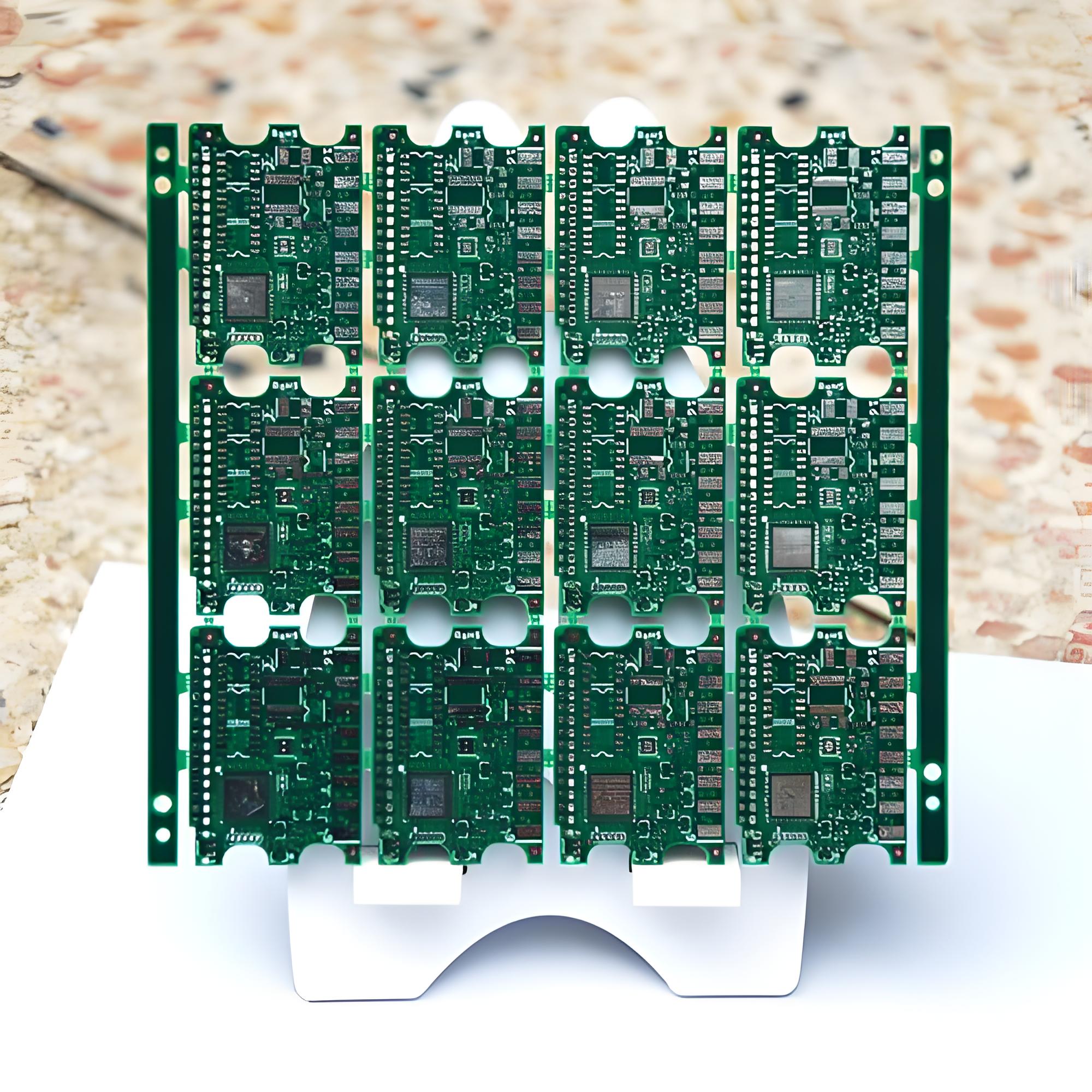
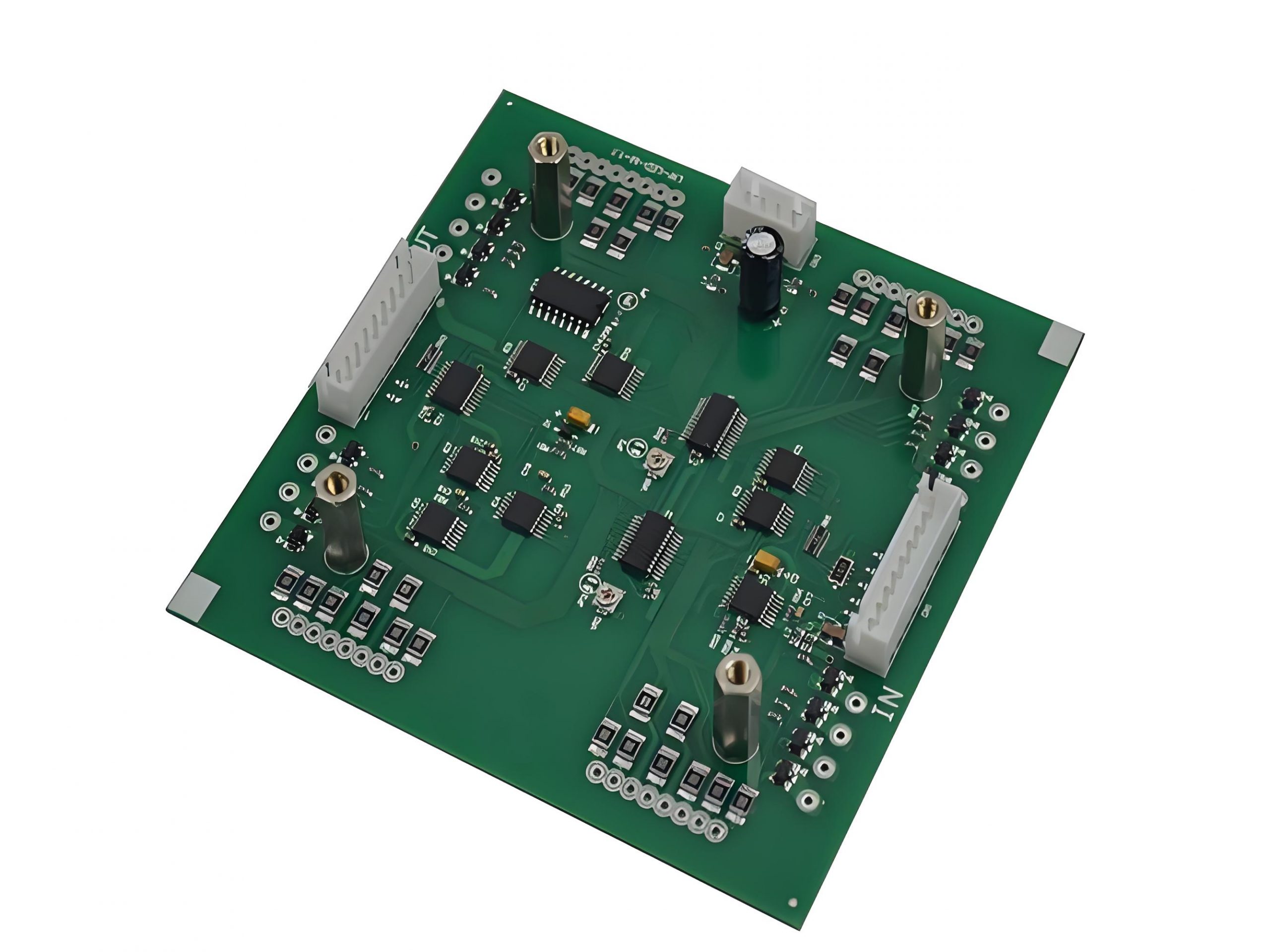
Green PCB board assembly refers to the process of attaching electronic components to a green PCB board to create a functional electronic assembly. This process of green PCB board involves several steps, starting with preparing the PCB, applying solder paste to the appropriate pads using a stencil, placing the components on the board using automated pick – and – place machines, and then reflow soldering to permanently attach the components. The assembly process requires precision and attention to detail to ensure that the components are placed correctly and that the solder joints are reliable. Quality control measures are an integral part of green PCB board assembly to detect any defects, such as misaligned components, cold solder joints, or solder bridges, and to ensure that the final assembly meets the required specifications.
How to Select A Reliable Green PCB Board Assembly Manufacturer?
Below are how to select a reliable green PCB board assembly manufacturer:
Experience and Reputation
- Industry Tenure: Manufacturers with 10+ years of experience often have optimized workflows. For example, companies that have navigated the transition from through – hole to SMT assembly can better handle complex designs.
- Case Study Analysis: Request detailed case studies of projects similar to yours. Look for examples where they overcame challenges like high – density component placement or mixed – technology assembly.
- Reference Checks: Contact at least three previous clients and ask about their experience with project timelines, defect rates, and how the manufacturer handled scope changes.
Quality Certifications
- ISO 9001: This standard ensures consistent quality management systems. A manufacturer with ISO 9001 should have documented processes for everything from incoming material inspection to final product testing.
- IPC – A – 610: As an industry – recognized acceptance criteria for electronics assembly, it defines acceptable soldering, component placement, and board cleanliness standards. Look for a manufacturer that goes beyond basic compliance and uses IPC-A -610 as a minimum benchmark for continuous improvement.
- Specialty Certifications: For green PCB assembly, certifications like RoHS (Restriction of Hazardous Substances) compliance are crucial. Some manufacturers may also hold UL (Underwriters Laboratories) or CE certifications relevant to your target market.
Technology and Equipment
- Pick – and – Place Machines: High – end machines, such as the Yamaha YSM series or Fuji NXT, offer placement accuracy down to 50 microns, essential for handling 0201 or smaller components. Ask about the machine’s feeder capacity and compatibility with different component packaging.
- Reflow Ovens: Advanced reflow ovens, like those with nitrogen – inerted chambers, can reduce oxidation during soldering, improving joint reliability. Inquire about the oven’s temperature profiling capabilities and how it can be customized for different solder alloys.
- Automated Optical Inspection (AOI): Modern AOI systems, equipped with 3D inspection technology, can detect hidden defects like tombstoning or insufficient solder volume. Check if the AOI system is integrated into the production line for real time defect identification.
Customization Capabilities
- Component Handling: A capable manufacturer should handle a wide range of components, including BGA (Ball Grid Array), QFN (Quad Flat No – lead), and fine – pitch connectors. Ask about their experience with components that require special handling, such as anti – static sensitive devices.
- Board Design Flexibility: Whether it’s a rigid – flex PCB or a high – layer count board, the manufacturer should be able to accommodate different form factors. Check their minimum and maximum board size limits, as well as their ability to handle complex geometries like blind and buried vias.
- Specifications Compliance: For electrical requirements, ensure they can meet impedance control tolerances (e.g., within ±5% for high – speed signals). On the mechanical side, they should be able to handle specific requirements like board thickness tolerances or mounting hole precision.
Production Capacity
- Throughput Analysis: Request data on their average daily or monthly production capacity for similar projects. A manufacturer that can handle 10,000+ boards per month may be suitable for large – scale production, but also consider their ability to scale up during peak demand.
- Flexibility in Production Runs: If you have varying production volumes, look for a manufacturer that offers both low – volume prototyping and high – volume production services. Some may even offer on – demand manufacturing to reduce inventory costs.
- Backup Capacity: Inquire about their contingency plans in case of equipment breakdowns or power outages. A reliable manufacturer should have backup power sources and spare equipment to minimize production disruptions.
Communication and Customer Service
- Project Management Tools: Manufacturers using tools like JIRA or Asana can provide real – time visibility into your project’s progress. Ask if they offer a client – accessible portal where you can view production schedules, test results, and shipping information.
- Dedicated Point of Contact: Having a single point of contact throughout the project can streamline communication. Ensure this person has technical knowledge to answer your questions about the assembly process.
- After – Sales Support: Post – production services, such as product repair or rework, are important. Check if they offer a warranty on their assembly services and what their turnaround time is for handling customer – reported issues.
Cost – effectiveness
- Total Cost Analysis: When comparing quotes, consider not just the unit price but also factors like setup costs, tooling charges, and shipping fees. A manufacturer with a slightly higher unit price may offer better value if they include free prototyping or lower tooling costs.
- Volume Discounts: For large – scale production, negotiate volume – based pricing. Some manufacturers may offer discounts starting at 1,000 units or more.
- Value – added Services: Look for manufacturers that provide cost – saving services, such as component sourcing. They may be able to negotiate better prices with suppliers due to their purchasing volume.
Supply Chain Management
- Component Sourcing: A reliable manufacturer should have partnerships with multiple component suppliers, including major distributors like Digi – Key and Mouser. This reduces the risk of component shortages and allows for quick substitution in case of unavailability.
- Inventory Management: Just – in – time (JIT) inventory systems can minimize material costs and lead times. Check if the manufacturer uses inventory management software to track component levels and ensure availability.
- Risk Mitigation: Ask about their contingency plans for supply chain disruptions, such as natural disasters or geopolitical events. A good manufacturer should have alternative sourcing strategies and safety stock policies.
Environmental Compliance
- Sustainable Materials: For Green PCB Assembly, ensure the manufacturer uses lead – free solders, halogen – free laminates, and recycled materials where possible. Look for documentation on the environmental impact of their materials.
- Waste Management: They should have proper procedures for handling hazardous waste, such as chemical solvents and metal scraps. Ask about their recycling programs and how they minimize waste generation during the assembly process.
- Energy Efficiency: Manufacturers that invest in energy – efficient equipment, like LED lighting in production areas or energy – saving reflow ovens, demonstrate a commitment to reducing their environmental footprint.
How to Achieve <10% Voiding in Green PCB Board BGA Assembly?
Here are methods about how to achieve <10% voiding in green PCB board BGA assembly:
Proper Solder Paste Selection
- Composition Analysis: Test multiple solder pastes with different flux contents (e.g., 8 – 12% flux by weight) and metal alloys (such as SAC305 – 96.5% Sn, 3.0% Ag, 0.5% Cu) in a small – scale trial run on sample Green PCB BGA assemblies. Record the voiding rates using X – ray inspection for each type. Select the paste that shows the lowest voiding rate in these tests.
- Supplier Collaboration: Work closely with solder paste suppliers to obtain datasheets and application notes specific to BGA assembly on Green PCBs. Suppliers may also offer technical support for optimizing paste usage.
Solder Paste Printing Optimization
- Stencil Thickness: Start with a standard stencil thickness for BGA components, usually 100 – 125 μm. For fine – pitch BGAs (pitch < 0.5 mm), consider using a thinner stencil (e.g., 80 μm). Adjust the thickness based on the results of solder paste deposit volume measurements using a profilometer.
- Aperture Design: Use a square – with – rounded – corners aperture shape for better paste release. For 0.5 mm pitch BGAs, start with an aperture size of 0.35 x 0.35 mm and fine – tune according to the actual solder paste transfer efficiency. Monitor the paste deposit shape and volume after each adjustment.
- Printing Parameters: Set the print pressure between 5 – 8 kg/cm² and the print speed at 30 – 50 mm/s. Make incremental changes (e.g., 0.5 kg/cm² for pressure and 5 mm/s for speed) and observe the impact on paste deposit quality. Use a stencil cleaning machine to clean the stencil every 5 – 10 prints to maintain consistent printing quality.
Component Placement Precision
- Machine Calibration: Regularly calibrate the pick – and – place machine using calibration tools provided by the manufacturer. Check the X, Y, and θ (rotation) axes for accuracy at least once a week.
- Vision System Setup: Optimize the vision system settings to accurately identify component fiducials and PCB pads. Use high – resolution cameras and appropriate lighting to ensure clear images. For BGAs, set the alignment tolerance to within ±50 μm.
- Placement Verification: Manually inspect the first few placed components on each batch using a microscope or an automated optical inspection (AOI) machine. Adjust the placement parameters if any misalignment is detected.
Reflow Profile Optimization
- Initial Profile: Start with a common reflow profile for Green PCB BGA assembly: a ramp – up rate of 1 – 2°C/s to reach the soak temperature of 150 – 180°C within 60 – 90 seconds, hold at soak for 60 – 120 seconds, a peak temperature of 217 – 230°C for 30 – 60 seconds, and a cooling rate of 2 – 4°C/s.
- Profile Tuning: Use a thermal profiler to measure the temperature at multiple points on the PCB during reflow. Analyze the temperature curves and adjust the ramp – up, soak, peak, and cooling rates based on the voiding results. For example, if there are excessive voids, try increasing the soak time or reducing the peak temperature slightly.
Stencil Design
- Aperture Count and Layout: Calculate the optimal number of apertures based on the BGA pad count and size. For large BGAs, consider using a stepped – aperture design to ensure even paste transfer. Use CAD software to design the stencil layout and perform a DFM (Design for Manufacturing) check before production.
- Stencil Material: Choose a stainless – steel stencil with an electro – polished surface for better paste release. For high – volume production, consider using a nickel – plated stencil for increased durability.
Component and Board Cleaning
- Pre – cleaning Inspection: Visually inspect the BGA components and Green PCBs under a microscope for any visible contaminants before cleaning.
- Cleaning Process: Use a cleaning agent compatible with the PCB and component materials, such as isopropyl alcohol (IPA) for water – soluble fluxes. For stubborn residues, consider using ultrasonic cleaning for 5 – 10 minutes. Rinse thoroughly with deionized water and dry using a hot – air gun or a drying oven at 60 – 80°C.
Humidity and Moisture Control
- Storage Conditions: Store BGA components and Green PCBs in a dry cabinet with a relative humidity (RH) level of < 20%. Use desiccant packs and humidity – indicating cards inside the storage containers.
- Handling Procedures: Before use, expose the components and boards to the production environment for at least 24 hours to allow them to equilibrate. If the components have been stored for more than the recommended time (usually 12 – 16 weeks), bake them at 125°C for 4 – 8 hours to remove any absorbed moisture.
In – Process Inspection
- X – ray Inspection Setup: Configure the X – ray inspection machine with appropriate imaging parameters, such as voltage (80 – 120 kV), current (50 – 100 μA), and magnification (10 – 50x) for clear visualization of voids in BGA joints.
- Inspection Frequency: Inspect every 10 – 20 boards in the assembly line. If voids are detected, increase the inspection frequency to every 5 boards until the issue is resolved.
Operator Training
- Theoretical Training: Provide a comprehensive training course covering the principles of Green PCB BGA assembly, including solder paste properties, reflow soldering, and component placement. Use training materials such as videos, slides, and textbooks.
- Practical Training: Have operators practice each step of the assembly process on sample PCBs under the supervision of experienced technicians. Provide feedback on their techniques and correct any mistakes immediately.
- Regular Refresher Courses: Conduct refresher courses every 3 – 6 months to reinforce the knowledge and skills of the operators and update them on any new processes or technologies.
Continuous Improvement
- Data Collection: Maintain a detailed database of all assembly runs, including the process parameters used, the number of voids detected, and the corrective actions taken.
- Root Cause Analysis: When voiding issues occur, use tools such as the 5 Whys, fishbone diagrams, or Pareto charts to identify the root causes. For example, if a high voiding rate is associated with a particular batch of solder paste, investigate the paste’s manufacturing process and storage conditions.
- Process Upgrades: Based on the root cause analysis, implement changes to the assembly process, such as upgrading equipment, changing suppliers, or modifying process parameters. Monitor the results of these changes to ensure a reduction in the voiding rate.
How to Achieve Green PCB Board Assembly Fast Delivery Without Affecting Quality?
Below are how to achieve green PCB board assembly fast delivery without affecting quality:
Efficient Project Management
- Assign a project manager with at least 3 years of PCB assembly experience. Use project management software like Jira to create a Gantt chart for the Green PCB Assembly process. Set up weekly review meetings to track progress against the timeline, and allocate resources based on the critical path of the project.
Streamlined Order Processing
- Implement an online order form that validates input fields in real – time. For example, if a component part number is entered, the system should check it against a database of available parts. Require customers to submit a detailed Bill of Materials (BOM) and PCB Gerber files at the time of order, and have an auto – response system that confirms receipt within 2 hours.
Inventory Management
- Analyze historical data to identify the top 20% of components used in 80% of Green PCB Assembly projects. Keep a 1 – month buffer stock of these components in a temperature – and humidity – controlled warehouse. Use an inventory management system that automatically reorders components when stock levels reach 30% of the buffer amount.
Automated Manufacturing Processes
- Install high – speed pick – and – place machines with a placement accuracy of ±0.05mm, such as the Yamaha YSM20. Equip the soldering area with reflow ovens that can handle lead – free soldering profiles precisely. Use automated optical inspection (AOI) machines after each assembly stage to catch 99% of visible defects immediately.
Concurrent Engineering
- Have the manufacturing team review the PCB design files within 48 hours of receiving them. Use design – for – manufacturability (DFM) software like Valor NPI to generate a report highlighting potential issues, such as component placement conflicts or soldering problems. Hold a joint design – manufacturing meeting to address these issues before starting production.
Express Shipping Options
- Partner with reliable courier services like DHL Express or FedEx Priority. For urgent orders, offer a guaranteed 24 – hour shipping option within the domestic market and 48 – hour international shipping. Provide customers with real – time tracking information and insurance coverage for the shipped Green PCBs.
Quality Assurance in Advance
- Conduct incoming inspection of all components using X – ray inspection for BGA components. Implement in – line testing during the assembly process, including flying probe tests for electrical connectivity. Have a final functional test using custom – made test fixtures before shipping the Green PCBs.
Supplier Collaboration
- Sign long – term contracts with at least 3 top – tier component suppliers. Set up a shared online portal where both parties can view inventory levels and production schedules. For critical components, negotiate a 2 – week lead time and a priority delivery option for emergency orders.
Flexible Production Scheduling
- Reserve 10% of production capacity for rush orders. Use a production scheduling software that can quickly re – allocate resources when an urgent order comes in. Train operators to be cross – skilled so that they can move between different production lines as needed.
Technology Adoption
- Subscribe to industry – leading PCB manufacturing magazines and attend trade shows like IPC APEX EXPO annually. Test new manufacturing techniques, such as 3D printing for prototyping or laser direct imaging for high – precision PCB production, in a pilot production line before full – scale implementation.
What Is the Difference Between Blue PCB and Green PCB?
Here are main difference between blue PCB board and green PCB board:
Visual Aesthetics and Design Preferences
- Green PCBs: Represent the industry standard, offering a classic appearance with high contrast between green solder mask and white silkscreen text. This combination enhances readability and reduces eye strain during prolonged inspection or assembly.
- Blue PCBs: Provide a modern, aesthetically distinctive look. The blue solder mask creates striking visual contrast with gold or silver components, making it popular in consumer electronics and devices aiming for a premium or innovative design.
Material Composition and Performance
- Green PCBs: Typically use epoxy resin-based solder masks with green pigments. These offer proven electrical insulation, moisture resistance, and thermal stability, making them reliable for general-purpose applications.
- Blue PCBs: Often utilize similar FR-4 substrates but with blue-tinted solder masks. They maintain comparable mechanical strength and durability while sometimes incorporating additives for enhanced UV resistance or cosmetic appeal.
Manufacturing Process and Cost
- Green PCBs: Benefit from mature, streamlined production processes. Green solder mask ink is mass-produced, resulting in lower material costs and faster lead times. This makes green PCBs the most economical choice for high-volume projects.
- Blue PCBs: Require specialized pigment formulations and may involve additional steps during solder mask application to achieve consistent coloration. While manufacturing costs are only marginally higher, custom color orders might incur slight premiums.
Application Suitability
- Green PCBs: Dominate in industrial controls, computer peripherals, and automotive electronics due to their balance of cost, performance, and ease of inspection. Their neutral tone also minimizes visual fatigue during assembly line work.
- Blue PCBs: Are favored in smartphones, wearables, and gaming hardware where product differentiation is critical. Their unique appearance aligns with branding strategies for tech-forward or lifestyle-oriented devices.
Inspection and Repair Considerations
- Green PCBs: The high contrast between green substrate and white markings simplifies automated optical inspection (AOI) and manual troubleshooting. Traces and components remain clearly visible under most lighting conditions.
- Blue PCBs: While still functional for inspection, the darker tone may slightly reduce visibility of fine-pitch traces or solder joints compared to green alternatives. This necessitates optimized lighting setups during quality control.
Environmental and Safety Factors
- Green PCBs: Use solder mask formulations that typically meet RoHS standards without requiring additional additives. Their composition minimizes outgassing risks during high-temperature processes.
- Blue PCBs: May incorporate cobalt or other pigments to achieve coloration, which could theoretically impact recycling processes if not properly managed. However, modern formulations mitigate most environmental concerns.
Conclusion
In conclusion, green PCB board stand out in electronics for their specialized materials, color – related properties, and distinct assembly methods. Main factors like choosing a trustworthy assembly manufacturer, optimizing BGA assembly voiding rates, and maintaining quality with fast delivery influence project outcomes. Understanding the nuances between blue and green PCB board also aids in making targeted choices.