

What is electrical bus bar? Let’s discover its definition, spec, types, sizing calculation and cleaning method through this blog.
Are you worried about these problems?
- How to achieve low-impedance, low-thermal-resistance electrical interconnection in high-density PCB layouts?
- How to rapidly verify mechanical compatibility between copper bars and PCBs during small-batch trial production?
- How to avoid material waste and delivery delays caused by traditional sheet metal processing?
As a electrical bus bar supplier, EBest Circuit (Best Technology) can provide you service and solution:
- Collaborative Design: Provide DFM simulation services to predict stress concentration at copper-PCB solder joints.
- Rapid Verification: 48-hour sample delivery with one-stop prototyping (laser cutting + surface treatment: tin/silver plating).
- Cost Optimization: Replace traditional machining with PCB etching process, boosting material utilization by 40%.
Welcome to contact us if you have any request for electrical bus bar: sales@bestpcbs.com.
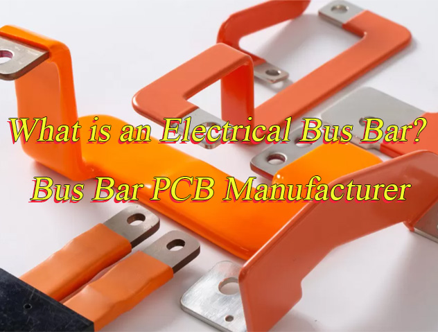
What is an Electrical Bus Bar?
Electrical Bus Bar is a core conductor in power systems for collecting, distributing, and transmitting electrical energy. Typically made of copper or aluminum with rectangular, circular, or tubular cross-sections, it concentrates power from sources like generators and transformers into a common conductor node, then allocates it via branch circuits to different load areas, enabling flexible energy dispatch.
Its low impedance minimizes energy loss while handling high currents, and modular design suits varied scenarios such as substations and switchgear. Structurally, bare conductors optimize heat dissipation, paired with insulators or metal enclosures for mechanical protection and safety isolation, making it vital for stable power transmission and system reliability.
Electrical Bus Bar Specification
| Parameter | Typical Value/Range |
| Base Metal | Copper (T2/TU1), Aluminum Alloy (6061/6101) |
| Surface Treatment | Tin Plating / Silver Plating / Insulating Paint Coating |
| Cross-Section Shape | Rectangular / Circular / Custom Shapes |
| Cross-Section Area Range | 10 mm² – 6000 mm² |
| Thickness Tolerance | ±0.05 mm (Precision Machined) |
| Rated Current (40°C) | 200A – 10kA |
| Short-Time Withstand Current | 10kA-100kA (1s) |
| Insulation Strength | AC 3kV-10kV/min No Breakdown |
| Tensile Strength | Copper ≥200 MPa, Aluminum ≥110 MPa |
| Bending Radius | ≤2× Thickness (Hard State) |
| Operating Temperature | -40°C ~ +125°C |
| Protection Level | IP00 (Bare Busbar) / IP2X-IP6X (With Enclosure) |
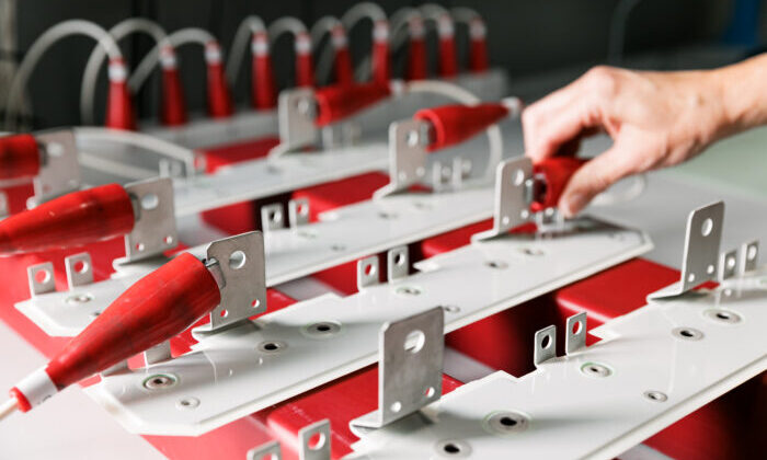
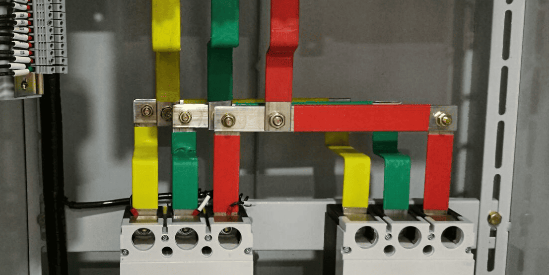
What Are Types of Electrical Bus Bars?
Copper Busbars
- Grades: TMY (hard copper busbar), TMR (soft copper busbar), T2, T3, TS, TSX, etc.
- Advantages: Extremely low resistivity (≈0.017241 Ω·mm²/m), excellent electrical conductivity, high mechanical strength, strong corrosion resistance, and high-temperature tolerance.
- Applications: High-current, space-constrained power distribution devices (e.g., high-voltage switchgear, main busbars from transformers to distribution rooms).
Aluminum Alloy Busbars
- Grades: AA6101, AA6201 (Al-Mg-Si series), aluminum-manganese alloy, aluminum-magnesium alloy, etc.
- Advantages: High strength (AA6101 tensile strength ≈220 MPa; AA6201-T81 up to 330 MPa), corrosion resistance, fatigue resistance, and superior electrical conductivity compared to pure aluminum (AA6101 conductivity ≈57.7% IACS).
- Applications: High-voltage overhead conductors, tubular busbars, channel busbars, and power distribution scenarios with high thermal/dynamic stability requirements.
Stainless Steel Busbars
- Grades: 304, 316, 430, etc.
- Advantages: Exceptional corrosion resistance (suitable for acidic/alkaline, humid, high-temperature environments), high strength, wear resistance, and compact structure.
- Applications: Harsh environments (chemical, marine, high-temperature industrial sectors).
How to Calculate Electrical Bus Bar Sizing?
1. Determine Current Carrying Capacity Requirements
- Bus bar dimensions must meet the system’s maximum operating current. Copper bus bars can use empirical formulas for estimation, e.g., single-layer copper bar capacity ≈ width (mm) × (thickness (mm) + 8.5) A (e.g., 100×10mm copper bar ≈ 1850A). Aluminum bars carry 70%-80% of copper’s capacity at the same size (divide by 1.3 for correction).
- Ambient temperature (40°C requires derating), cooling conditions (enclosed busways have poorer heat dissipation), and multi-layer configurations (double-layer ≈1.5× single-layer capacity).
2. Thermal Stability Verification
- Short-Circuit Withstand: Validate thermal effects during faults. Formula: Cross-section S (mm²) = I (kA) / a × √(t / Δθ), where:
- I: Rated short-time withstand current (e.g., 31.5kA);
- a: Material coefficient (13 for copper, 8.5 for aluminum);
- t: Fault duration (typically 4s);
- Δθ: Allowable temperature rise (180K for bare copper at 4s, capped at 215K).
- Example: 6×60mm copper bars can withstand ~31.5kA short-circuit current (thermal stability verified).
3. Temperature Rise Limitations
- Standard Values: Copper bus bars ≤60K (bare), ≤65K (tin-plated), ≤70K (silver/nickel-plated); Aluminum ≤50K (Indian standard at 35°C ambient).
- Calculation: τ = I²ρ(1+αθ)/(KtM), where ρ = resistivity, Kt = heat dissipation coefficient, M = cross-section perimeter. Copper temperature rise is proportional to resistivity; aluminum rises ~40% higher than copper at the same current due to higher resistivity.
4. Material Selection & Grades
- Copper Bus Bars: T2/TU1 electrolytic copper (≥97% IACS conductivity, ≥200MPa tensile strength) for high-voltage switchgears (≥3000A) and data centers. Silver plating reduces contact resistance to <2μΩ for high-frequency applications.
- Aluminum Bus Bars: 6061-T6 (≥240MPa strength, ≥50% IACS conductivity) and 6101 (≥55% IACS conductivity) for lightweight (30% of copper density) and cost-effective solutions. Requires friction welding or coated bolts to prevent galvanic corrosion, ideal for EV battery packs and PV DC sides.
5. Cross-Section Shape & Installation
- Shape Selection: Rectangular bars (aspect ratio ≤1:5) offer 20-30% higher capacity than circular bars of the same area; circular bars excel in vibration resistance; custom shapes (e.g., L-type) fit complex spaces. PV inverters often use laminated insulated bars (1500VDC withstand).
- Installation Impact: Horizontal installation improves heat dissipation vs. vertical; enclosed busways require 10-20% capacity derating due to poor cooling.
6. Mechanical Strength & Bending Radius
- Mechanical Requirements: Copper ≥200MPa, aluminum ≥110MPa tensile strength. Hard-state bars require bending radius ≤2× thickness to avoid cracks; flexible braided copper foil (multi-layer) allows bending to ≤2× thickness for space-constrained areas.
- Support & Fixing: Insulator spacing must withstand dynamic loads (e.g., short-circuit forces); bolt torque must resist electrodynamic loads to prevent loosening or overheating.
7. Environmental & Code Compliance
- Environmental Factors: High altitudes require capacity derating (1-2% per km); humid/corrosive environments need tin/silver plating.
- Standard Alignment: Follow GB/T 5585.1-2018, IEC 60439, etc., incorporating system voltage (e.g., 10kV) and short-circuit capacity (transformer rating + impedance) for validation.
How to Clean Electrical Bus Bar?
1. Power Disconnection & Safety Verification
- Disconnect power supply to busbar and associated equipment. Verify absence of voltage using 1000V voltage tester. Install “DO NOT OPERATE” warning signs and grounding wires.
- Operate only in environments with humidity ≤70%. Avoid rain, lightning, or wet conditions. Wear insulated gloves, safety goggles, and non-conductive footwear.
2. Initial Surface Cleaning
- Remove dust, metal debris, and contaminants from busbar surface, enclosures, ventilation holes, and joints using industrial vacuum cleaners or soft-bristle brushes.
- For stubborn stains, use compressed air or EC0102 specialized electrical cleaning agent (non-aqueous, non-flammable). Avoid water-based or flammable cleaners.
3. Joint Deep Cleaning & Maintenance
- Inspect and tighten connection bolts/spring washers using torque wrench (e.g., 25-30N·m for M8 bolts). Replace degraded insulators, clamps, and temperature-sensitive wax markers.
- Treat oxidation: Remove aluminum oxide layer with wire brush, then apply petroleum jelly. For copper busbars, apply tin plating (0.1-0.15mm thickness) and conductive paste for corrosion protection.
- Verify joint clearance ≤0.05mm using 0.05mm feeler gauge.
4. Oil & Corrosion Treatment
- For heavy oil contamination, use suction gun with cleaning agent or LE-50 live-line cleaning cloth (power-off operation required).
- For corroded areas: Sand smooth, apply conductive paste/grease to prevent moisture/chemical ingress.
5. Insulation Performance Testing
- Measure busbar-to-ground and phase-to-phase insulation resistance using 1000V megohmmeter. Requirements: ≥0.5MΩ for LV, ≥10MΩ for HV/enclosed busbars.
- If resistance fails standards, troubleshoot moisture, contamination, or aging issues. Dry or replace insulation materials as needed.
6. Thermal Management System Maintenance
- Clear ventilation holes, cooling fins, and air ducts to prevent blockages. Monitor temperature at designated points (every 10-15m) with operational limits ≤70-90°C (material-dependent).
7. Final Inspection & Recommissioning
- Confirm no cleaning agent residue or debris remains. Remove grounding wires/warning signs.
- Conduct no-load test run before re-energizing. Monitor current, temperature, and insulation resistance data to ensure normal operation.
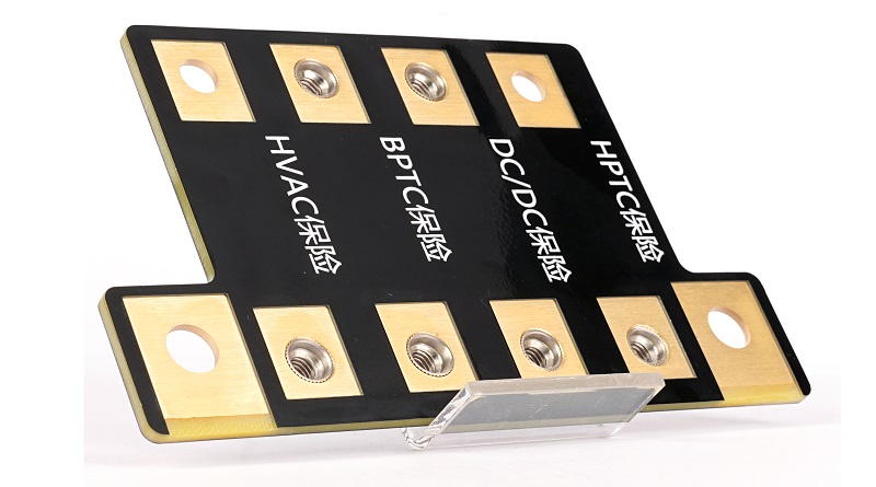
Why Choose Bus Bar PCB?
- High Current Capacity, Lower Losses: Thick copper layers (≥2oz) handle hundreds to thousands of amps, reducing voltage drop and power waste, ideal for high-power applications like server power supplies and EV battery systems.
- Compact Design, Space Savings: Integrated bus bars replace bulky cables and connectors, cutting PCB area by 30%+ and enabling smaller, denser designs for devices like data center power modules.
- Better Heat Dissipation: Copper’s high thermal conductivity quickly transfers heat from components (e.g., MOSFETs), lowering temperatures and extending device life while reducing reliance on active cooling.
- Cost-Effective Manufacturing: Standardized bus bar modules and automated assembly streamline production, cutting labor costs and shortening lead times, beneficial for mass production and quick iterations.
- Improved EMC Performance: Shielding layers and optimized grounding reduce high-frequency noise and EMI, ensuring cleaner signals and easier compliance with EMC standards in high-speed circuits.
- Flexible & Scalable Design: Custom shapes, sizes, and connection types (e.g., plug-in, soldered) adapt to device needs. Modular designs allow easy adjustments for power upgrades or interface changes.
- Reliable in Harsh Environments: Tested for durability in extreme conditions (-40°C to 125°C, humidity, salt spray), ensuring stable operation in industrial controls, aerospace, and automotive systems.
How to Design Electric Bus Bar PCB?
1. Define Design Parameters & Boundary Conditions
- Calculate target current capacity: Based on load power (P=UI) and allowable voltage drop (ΔV≤1%), derive busbar cross-sectional area (A=I/(K·σ)), where K is conductivity coefficient (copper: 58A/mm²) and σ is allowable temperature rise coefficient (typically ≤30℃).
- Determine voltage class and insulation requirements: High-voltage scenarios (>600V) require thickened insulation layer (≥100μm) and creepage distance design (e.g., ≥8mm/kV), while low-voltage scenarios allow optimized space layout.
2. Material & Stack-Up Structure Selection
- Copper foil thickness: ≥2oz (70μm) for high-current paths, 1oz for signal layers. Aluminum/copper substrates are used for high-heat scenarios (e.g., power modules), paired with thermal interface material (thermal conductivity ≥1.0W/m·K).
- Layer stack design: Adopt “power-ground-signal” layered layout. Busbar trace width ≥3mm (for currents ≥50A), spacing ≥2mm (to prevent arcing). Embedded busbars require reserved assembly holes and positioning markers.
3. Thermal Management & Heat Dissipation Design
- Thermal simulation verification: Use ANSYS Icepak or equivalent tools to simulate busbar temperature distribution, ensuring hotspots ≤90℃ (copper melting point 1083℃, with safety margin).
- Heat dissipation path optimization: Add thermal pads on the back of busbars (copper area ≥300mm²), connected to bottom-layer heat sinks via thermal vias (via diameter ≥0.3mm, spacing ≤1mm). Liquid cooling channels are designed below busbars, with channel width ≥5mm and flow rate ≥0.5m/s.
4. Electrical Performance & EMC Optimization
- Impedance matching design: Busbar trace length ≤1/10 wavelength (to avoid resonance), with decoupling capacitors (100nF-10μF) added at critical nodes.
- EMI suppression measures: Surround busbars with grounded shielding layers (copper coverage ≥80%), add ferrite beads/common-mode chokes on high-frequency paths, and use orthogonal routing between signal and power layers to reduce crosstalk.
5. Design for Manufacturing (DFM) & Test (DFT)
- Manufacturing process verification: Confirm etching accuracy (trace width/spacing tolerance ±10%), plating uniformity (copper thickness variation ≤10%), and lamination alignment (±50μm).
- Test point design: Reserve test pads (diameter ≥2mm) at critical busbar nodes, using 4-wire measurement to avoid contact resistance errors. High-voltage scenarios require added insulation resistance test points (≥1 per 100mm² busbar).
6. Prototype Validation & Iteration
- Engineering sample fabrication: Use LDI (Laser Direct Imaging) for high precision, verify electrical connections via flying probe testing.
- Performance testing: Measure busbar voltage drop (≤0.5% rated voltage), temperature rise (≤30℃), and insulation resistance (≥100MΩ@500V DC) under ambient/high-temperature conditions. EMC testing must comply with CISPR 22/25 standards.
- Iteration optimization: Adjust trace width/heat dissipation structure based on test results (e.g., increase copper thickness for excessive temperature rise, add shielding layers for EMI issues).
7. Environmental & Reliability Enhancement Validation
- Execute environmental stress tests: Temperature cycling (-40℃~125℃ for 100 cycles), humidity test (85℃/85% RH for 96h), vibration test (5-500Hz sweep, 3-axis 2h each), and salt spray test (120h neutral salt spray).
- Reliability accelerated life testing: Use HAST (Highly Accelerated Stress Test) or THB (Temperature Humidity Bias Test) to validate insulation material stability under long-term high-humidity/high-temperature conditions.
- Failure mode analysis: Conduct root cause analysis for issues identified during testing (e.g., solder joint voiding, insulation breakdown), and optimize design (e.g., increase pad copper thickness, optimize insulation layer thickness).
Why Choose EBest Circuit (Best Technology) as Bus Bar PCB Manufacturer?
Reasons why choose us as bus bar PCB manufacturer:
- 19 Years of Expertise: Leveraging 19 years of PCB manufacturing experience and a process database for full-process material selection and parameter guidance, reducing trial-and-error costs.
- Cost-Competitive Solutions: Cost-sensitive design optimization and tiered pricing system reduce unit costs by 15%-30% while maintaining performance, maximizing project budget efficiency.
- 24-Hour Rapid Prototyping: Dedicated green channel for urgent orders ensures sample fabrication and testing within 24 hours, cutting product development cycles by over 40%.
- 99.2% On-Time Delivery Rate: Smart production scheduling and real-time logistics monitoring guarantee 99.2% of orders arrive on schedule, preventing project delays and market opportunity losses.
- 100% Full-Process Inspection: AOI/X-Ray smart detection and 100% inspection from raw materials to finished goods ensure defect rates ≤50ppm.
- Authoritative Certifications: Compliance with ISO 9001/ISO 14001, IATF 16949 automotive, ISO 13485 medical, and RoHS 2.0 standards meets global industry compliance requirements.
- Production Error Database: Historical defect database with big data analysis predicts risks, saving clients over 2 million annually in quality-related losses.
- Free DFM Analysis: Pre-production design optimization identifies over 95% of potential process issues, minimizing mass production risks.
- One-Stop Solutions: Integrated design-manufacturing-testing-logistics services eliminate multi-vendor coordination, boosting project management efficiency by 30%.
- Custom Technical Support: Dedicated engineer teams provide 24/7 support from concept validation to mass production tracking, ensuring precise design intent realization.
Welcome to contact us if you have any request for bus bar PCB: sales@bestpcbs.com.