How to design 20 oz copper PCB for high current? Let’s explore thickness, specifications, benefits, application and design guideline for 20 oz copper PCB.
Are you worried about these problems?
- PCB circuits are prone to overload and burn in high current scenarios.
- The heat dissipation solution takes up space and is expensive.
- The yield rate of thick copper plate processing fluctuates greatly.
The services EBest Circuit (Best Technology) can provide:
- The 20oz ultra-thick copper foil design has a current carrying capacity that is 3 times that of conventional PCBs. It can stably carry 150A continuous current through thermal simulation verification.
- The patented copper-based composite structure and built-in heat conduction channel realize PCB self-heating, saving 40% of the cost of peripheral heat dissipation components.
- The unique step-by-step pressing process, combined with full-process quality control, ensures that the batch production yield rate is stable at more than 95%.
Welcome to contact EBest Circuit (Best Technology) if you have any inquiry for copper PCB: sales@bestpcbs.com.
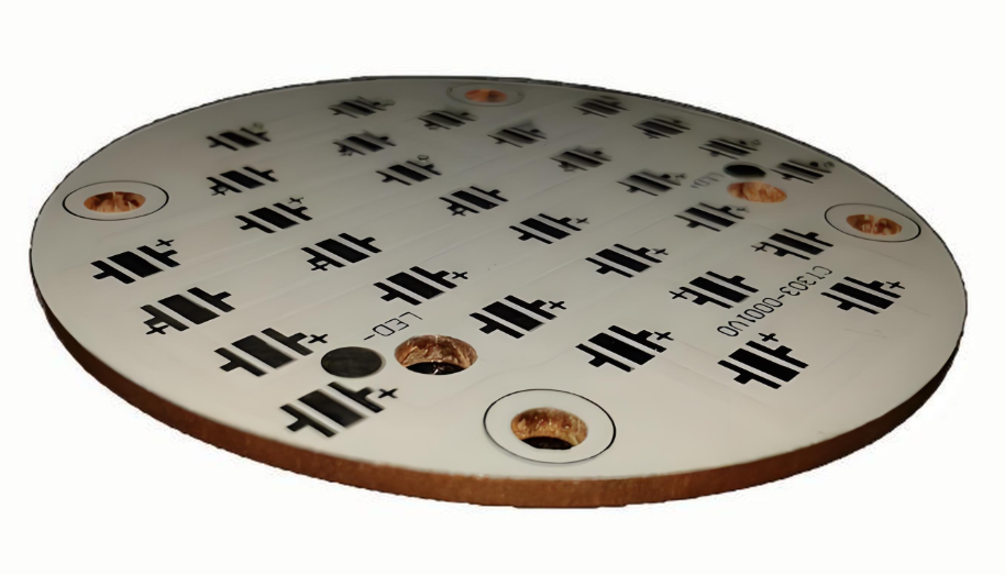
What Is a 20 oz Copper PCB?
A 20 oz copper PCB utilizes a 700μm-thick copper layer (equivalent to 20 ounces per square foot), significantly exceeding standard copper weights to achieve exceptional electrical performance. This extreme copper thickness minimizes resistive losses (I²R heating) while enabling current handling capabilities exceeding hundreds of amperes, making it essential for high-power systems requiring stable operation under intense loads.
Its substantial copper mass provides superior thermal conductivity (>380 W/m·K), efficiently dissipating heat toward heatsinks or enclosures to maintain operating temperatures within safe limits. Fabrication demands specialized processes like stepped lamination and high-temperature resins to prevent delamination, ensuring structural integrity during repeated thermal cycles. These boards serve critical roles in electric vehicle charging systems, industrial power converters, and energy distribution infrastructure where reliability under sustained high loads is non-negotiable.
How Thick Is 20 oz Copper PCB?
The thickness of a 20 oz copper layer in a PCB is approximately 700 micrometers (μm) . This measurement is derived from the industry standard where 1 ounce (oz) of copper per square foot equals roughly 35 μm in thickness, utilizing copper’s density and unit conversion principles.
Due to manufacturing tolerances, the actual copper thickness may vary by ±10%, resulting in a typical range of 630 μm to 770 μm for 20 oz copper PCBs.
20 oz Copper PCB Specifications
| Parameter | Specification |
| Copper Thickness | 700μm (20 oz) ±10% |
| Current Capacity | 100A+ continuous |
| Base Material | 1-3mm thick copper core (99.95% purity) |
| Thermal Conductivity | 400W/(m·K) (copper core) |
| Insulation Layer | 50-100μm ceramic (Al₂O₃/AlN), >3kV breakdown |
| Min Trace Width | 12mil (0.3mm) |
Benefits of 20 oz Copper Base PCB
- Extreme Current Handling – Supports 100A+ continuous current (3x standard PCBs), ideal for high-power applications like EV chargers and industrial inverters.
- Superior Thermal Management – Copper core dissipates heat 60% faster than aluminum, reducing hotspots and extending component lifespan.
- Space-Saving Design – Thick copper (700μm) allows narrower traces (12mil vs. 6mm for equivalent current), saving PCB area.
- High Reliability – Resists thermal cycling fatigue, 3x longer lifespan in high-temperature environments vs. standard PCBs.
- Lower Resistance – Pure copper base reduces conductive losses by 40%, improving energy efficiency.
- High-Frequency Performance – Smooth copper surface (Ra<0.5μm) minimizes signal loss for RF/5G applications.
- Mechanical Strength – Copper core prevents warping under heavy components (e.g., IGBT modules).
When to Use 20 oz of Copper PCB?
Applications of 20 oz copper PCB:
- High-Power Electronics – Ideal for EV charging systems, industrial motor drives, and power converters requiring minimal resistance and efficient heat dissipation.
- RF & Telecommunications – Best for 5G base stations and satellite communication equipment where signal integrity and thermal stability are crucial.
- Heavy-Duty Power Switching – Suitable for welding machines, server power supplies, and UPS systems handling extreme current surges.
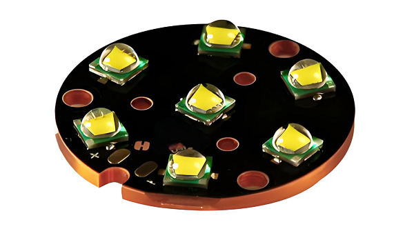
- High-Brightness LED Systems – Used in stadium lighting and industrial LED arrays where active cooling is necessary to maintain performance.
- Automotive Power Modules – Optimal for EV inverters and battery management systems needing compact, high-current designs.
- High-Temperature Industrial Equipment – Applied in machinery where prolonged thermal cycling and reliability are key factors.
What Is Difference between 16 oz and 20 oz Copper PCB?
| Comparison Aspect | 16 oz Copper PCB | 20 oz Copper PCB |
| Copper Thickness | ~560 μm | ~700 μm |
| Current Carrying Capacity (at same trace width) | Handles high currents (e.g., ~80A for 10mm width) | Handles high currents (e.g., ~80A for 10mm width) |
| Thermal Management | Good heat dissipation, suitable for moderate-power apps | Superior heat spreading, minimizes hotspots by 15-20% |
| Space Efficiency (trace width for same current) | Requires wider traces (e.g., 6mm for 30A) | Enables narrower traces (e.g., 4.8mm for 30A), saving PCB area |
| Manufacturing Cost & Difficulty | Higher cost than standard PCBs, moderate etching challenges | Highest cost due to complex etching and material use |
| Applications | Industrial motor drives, UPS systems | EV fast chargers, server power supplies (>500A surges) |
How to Design 20 oz Copper PCB for High Current?
20 oz Copper PCB design guideline for High-Current
1. Copper & Trace Design
- Current Capacity: Use I = 0.048×ΔT^0.44×(W×H)^0.725 (IPC-2221). 20 oz copper (700µm): 15mm width supports ~100A at ΔT=30°C.
- Trace Compensation: 2 oz: Add 0.2mm width; spacing ≥0.25mm; 4 oz: Critical traces ≥1.5mm wide; spacing ≥0.4mm.
- Plane Layers: Use full-layer planes for currents >30A (lower impedance, better heat spread).
2. Thermal Management
- Via Arrays: Place ≥0.3mm vias under power devices (pitch ≤1.5mm). Fill with thermal paste to connect to bottom copper, cutting thermal resistance by >50%.
- Exposed Copper: Remove solder mask for direct air cooling (2–3× heat dissipation). Apply ENIG/HASL for oxidation resistance.
- Embedded Copper: For >50A, embed 1.5mm copper blocks in FR4 layers (reduces local temps by ≥30°C).
3. Layer Stackup
- Multilayer Structure: “Sandwich” stackup (power layer – insulating layer – 2 oz copper + 1mm aluminum). Inner layers use stepped copper (0.5–4 oz) to reduce Z-axis stress.
- Prepreg: High-resin (e.g., 2116) for 85%+ fill. Board edges reinforced with epoxy slots (30% stronger).
4. Manufacturing
- Etching/Plating: Use LDI for 3/3mil traces; pulse plating for ≥25µm hole copper (uniformity >90%).
- Lamination: Pre-press 180°C/40min/15kg/cm²; full press 200°C/90min/25kg/cm²; cool ≤3°C/min.
5. Safety & Compliance
- Clearance: AC/DC ≥6mm; creepage ≥8mm/1000V (IEC 60664).
- Protection: 132°C TCO + current sensor; TVS diodes ≤5mm from connectors.
- Isolation: Optocouplers/transformers for AC-DC; primary-secondary spacing ≥8mm.
6. Verification
- Thermal Sim: ANSYS Icepak/Simcenter for device temps (MOSFET Tj <125°C). Current Density: SIwave maps; avoid >500A/cm² (prevents electromigration).
- Testing: Infrared scan for hotspots; key paths ΔV <2% (e.g., <0.24V for 12V).
Client Design Tips:
- Cost vs. Performance: 20 oz suits 50A+ but needs via arrays/aluminum.
- Fabricator: Choose LDI/pulse-plating vendors.
- Lead Time: Add 3–5 days for custom stacks; confirm impedance upfront.
Why Choose EBest Circuit (Best Technology) as Your Copper PCB Manufacturer?
- 24-hour rapid prototyping: shorten the R&D cycle by 50% and accelerate product launch.
- 1 Piece MOQ & Competitive Pricing – No hidden costs, offering the best value without compromising quality.
- Thermal Solution Consulting: Free CFD simulation identifies optimal airflow paths.
- Turnkey Solutions – Full-service PCB manufacturing from design to delivery, accelerating your product’s time-to-market.
- ISO 14001/ISO 13485 certification: medical/automotive customers are exempt from secondary testing, and compliance costs are reduced by 30%.
- Free DFM (Design for Manufacturability) Analysis: Optimizes PCB layouts to reduce material waste, lower production costs, and avoid late-stage design revisions.
- Rigorous quality control: directly reducing your maintenance costs by 40% while extending product lifespan.
If you have any request for copper base PCB, welcome to contact us to get a free quote: sales@bestpcbs.com.