

Why choose copper deposition PCB for HDI board? Let’s explore technical parameter, benefits, production process, optimization solutions for copper deposition PCB.
Are you troubled with these problems?
- How to ensure even copper deposition for HDI boards?
- How to prevent signal loss from excessive copper thickness?
- How does incomplete microvia filling affect PCB reliability?
EBest Circuit (Best Technology) can provide service and solution:
- Precision Thickness Control – Pulse plating ensures ±5% copper thickness tolerance.
- Microvia Fill Technology – High-ductility copper eliminates voids, boosting yield by 15%.
- Eco-Friendly Additives – Cyanide-free plating reduces wastewater treatment costs, RoHS compliant.
Welcome to contact us if you have any request for copper deposition PCB: sales@bestpcbs.com.
What is Copper Deposition PCB?
Copper deposition PCB is a circuit board manufacturing technology that deposits a copper layer on the substrate surface through electrolytic or chemical methods. This technology is categorized into two main types: electroplated copper (which requires a conductive layer and is used for through-hole plating and surface thickening) and electroless copper (which does not require a conductive layer and is suitable for metallizing non-metallic substrates such as plastics).
This process directly impacts the PCB’s conductivity, signal transmission speed, and structural reliability. It is a core technology for achieving high-density interconnect (HDI), flexible circuits, and electromagnetic shielding. It is widely used in 5G communications, automotive electronics, and consumer electronics.
Copper Deposition PCB Technical Parameter
| Parameter Category | Technical Specifications |
| Copper Layer Thickness | Electroless: 0.3–1μm (0.01–0.03oz) |
| Electrolytic: 5–70μm (1–3oz) | |
| Thick Copper: Max 30oz (≈1050μm) | |
| Plating Uniformity | Hole wall copper thickness variation ≤15% |
| Surface copper tolerance ±10% | |
| Current Carrying Capacity | 1oz (35μm): 1.8A/mm² |
| 2oz (70μm): 3.6A/mm² | |
| 3oz (105μm): 5.4A/mm² | |
| Surface Roughness | Electrolytic Foil: Ra 0.8–1.2μm |
| Rolled Foil: Rz ≤3μm | |
| Tensile Strength | Electrolytic Foil: 150–300MPa |
| Rolled Foil: Elongation 20–40% | |
| Min Line Width/Spacing | Inner Layers: 0.05mm |
| Outer Layers: 0.065mm | |
| Hole Metallization | Mechanical Drill: ≥0.15mm |
| Laser Drill: ≥0.05mm | |
| Aspect Ratio ≤8:1 |
Why Choose Copper Deposition PCB for HDI Board?
Electrical Conductivity & Signal Integrity
- High Copper Conductivity: Minimal resistive losses (I²R) reduce line heating.
- Microvia Direct Connections: Shorten signal path lengths by >30%, eliminating high-speed signal bottlenecks.
Thermal Management & Longevity
- Thermal Conductivity: Exceeds aluminum (380-400 W/m·K), ensuring efficient heat dissipation for high-power components.
- Thermal Stability: Low CTE (Coefficient of Thermal Expansion) minimizes solder joint fatigue under thermal cycling (-40°C~+125°C).
Space Efficiency & Component Density
- Laser-Drilled Microvias: Filled with copper, enabling board thickness reduction to 0.4mm (vs. standard 0.6mm).
- Copper-Pillar Interconnects: Replace traditional through-holes, achieving 30% higher component density.
Cost & Manufacturing Efficiency
- Layer Reduction: 6-layer HDI design achieves equivalent performance of 8-layer conventional boards.
- High Yield Rates: Mature electroless/electrolytic copper processes reduce rework (defect rate <0.2%).
Durability & Environmental Resistance
- Mechanical Robustness: Withstands 1.5m drop tests and 50G vibration loads (industrial/automotive grade).
- Humidity/Temperature Resistance: Maintains functionality in 95% RH and 85°C environments (IEC 60068-2-30).
Design Flexibility
- Hybrid Architecture: Combines HDI zones (for 5G antennas/chip packaging) with conventional FR4 regions.
- Thick Copper Integration: Supports 10oz+ copper layers for high-current power modules (≥200A).
How is Copper Deposited on HDI Board?
Copper Deposition Process for HDI Boards
1. Drilling
- Laser (CO₂/UV) or mechanical drilling creates microvias (blind/buried holes) for interlayer connections. UV lasers achieve finer apertures (e.g., <25μm) with minimal thermal damage.
2. Desmear & Cleaning
- Alkaline potassium permanganate treatment removes drilling residues, followed by cleaning to ensure contamination-free surfaces for metallization.
3. Chemical Roughening
- Micro-etching (sulfuric acid/hydrogen peroxide) roughens copper surfaces (2-3μm depth) to enhance adhesion between the electroless copper layer and substrate.
4. Activation
- Colloidal palladium activation deposits catalytic particles on non-conductive via walls, replacing outdated sensitization methods for reliable adhesion and avoiding copper displacement issues.
5. Electroless Copper Plating
- A thin conductive layer (0.5-1μm) is deposited via autocatalytic reduction (copper ions + formaldehyde reductant) to initiate conductivity on via walls.
6. Electroplating Copper Thickening
- Pulse electroplating adds 20-30μm copper to fill vias and reinforce conductivity. Parameters: current density 2-3A/dm², copper concentration 28-32g/L, temperature controlled.
7. Pattern Transfer & Etching
- Photoresist coating, exposure, and development create circuit patterns. Wet/dry film etching removes excess copper, retaining designed traces.
8. Lamination & Stacking
- Prepreg layers and core boards are vacuum-laminated under high temperature (180-190°C) and pressure (90-min curing) to form multilayer structures.
9. Surface Finish(Optional)
- OSP: Organic solderability preservative (cost-effective, oxidation-resistant).
- ENIG: Electroless nickel immersion gold (superior conductivity for high-frequency signals).
- Immersion Ag/Au: Enhanced solderability (Ag requires anti-tarnish measures).
- HASL: Hot air solder leveling (traditional, lower cost but less flatness).
10. Quality Inspection
- AOI, X-Ray (via filling check), electrical tests (continuity, impedance), and reliability trials (thermal stress, salt spray) ensure compliance.
Copper Deposition Optimization for HDI Inner Layer Circuits
1. Plating Solution Formulation Optimization
- Adjust copper salt concentration and additive ratios (e.g., levelers, suppressors) to balance deposition rate and uniformity.
- Introduce chloride-based carriers to enhance throwing power and reduce void defects in via filling.
2. Substrate Surface Preparation
- Use plasma or chemical roughening to improve copper-substrate adhesion.
- Ensure strict cleaning (oxide/organic residue removal) to prevent discontinuous deposition or delamination.
3. Process Parameter Control
- Apply dynamic current density (pulsed plating) to optimize copper thickness distribution across hole walls and surfaces.
- Maintain temperature at 20–25°C to avoid crystal structure defects from precipitate formation.
4. Equipment & Flow Design
- Upgrade plating tank agitation (jet + vibration systems) to minimize edge effects and thickness variation.
- Use high-purity titanium anode baskets with soluble anode membranes for ion balance maintenance.
5. Inline Monitoring & Feedback
- Deploy real-time resistivity sensors for automated additive replenishment based on solution composition.
- Integrate laser thickness gauges for closed-loop control, reducing post-plating grinding loss.
6. Sustainability & Cost Efficiency
- Develop low/cyanide-free plating systems to cut wastewater treatment costs.
- Optimize plating tank load (≥80%) to minimize copper ball consumption and downtime.
7. Failure Mode Analysis
- Build defect databases (nodules, pinholes) using DOE to identify critical process windows.
- Regularly test ductility (≥15%) and resistivity (≤2.0μΩ·cm) for reliability assurance.
Long-Term Reliability of HDI Boards via Copper Deposition
1. Grain Structure Optimization
- Control copper grain size (<5μm) and directional alignment to reduce grain boundary sliding under thermal stress.
- Use pulsed plating for denser grains, lowering fatigue crack initiation risk.
2. Additive Residue Management
- Monitor decomposition byproducts of organic additives (e.g., suppressors, brighteners) to prevent electrochemical migration.
- Apply activated carbon filtration for ≥99.9% purity.
3. Thermal Stress Mitigation
- Add graded metal layers (e.g., Ni/Au) between copper and substrate to address CTE mismatch.
- Validate solder joint reliability via thermal cycling (-55°C to 125°C), targeting ΔTg ≤5°C.
4. Environmental Resistance
- Limit porosity (<2 defects/cm²) to block moisture-induced corrosion.
- Post-plate baking (150°C/2h) removes residual moisture for humidity resistance.
5. Electromigration Prevention
- Optimize copper thickness uniformity (±3μm) to avoid high current density zones.
- Use Co/Pd alloy barriers to extend MTBF >20 years.
6. Dynamic Load Monitoring
- Embed fiber optic sensors for strain distribution tracking (resolution ≤1με).
- Predict remaining lifespan via ML with <10% error margin.
7. Standards Compliance
- Meet IPC-6012DS: peel strength ≥1.4N/mm, solderability at 260°C/10s.
- Third-party testing (UL/CSA) confirms ≤5% electrical degradation after 125°C/1000h aging.
Our Copper Deposition HDI Board Case Studies
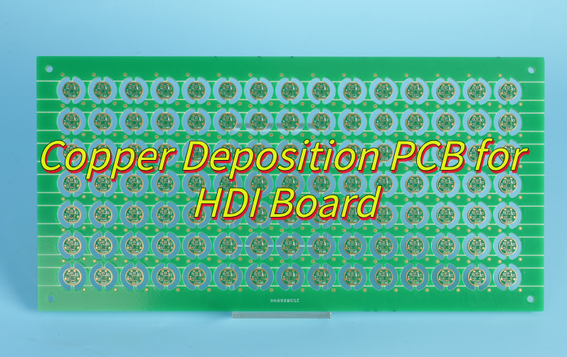
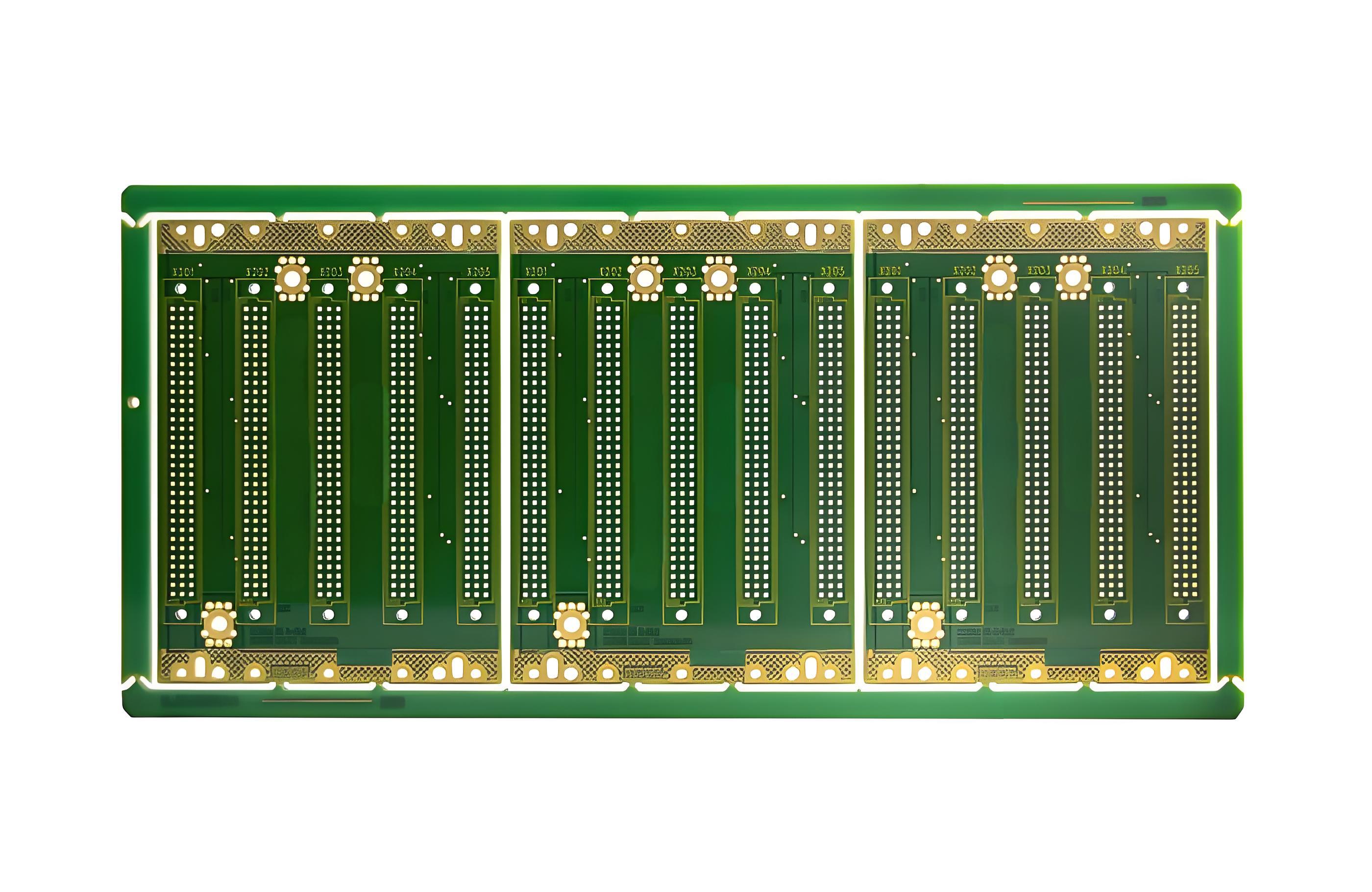
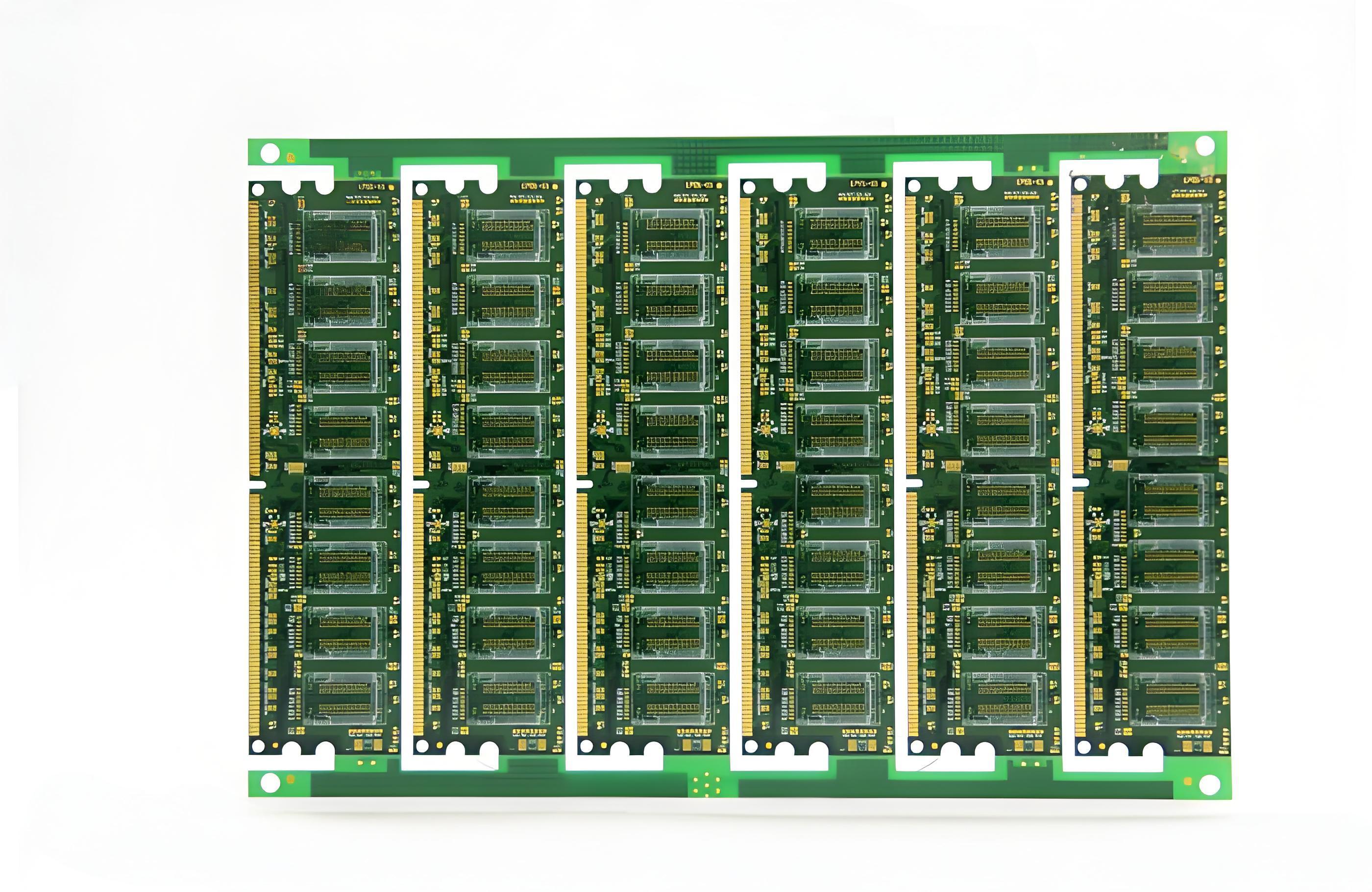
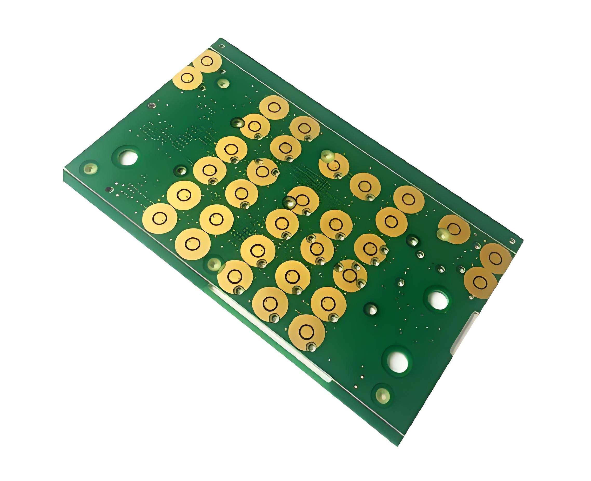
With 19 years of specialized experience in copper deposition for HDI boards, we have successfully delivered thousands of projects across industries. Our expertise spans from precision electroplating and microvia filling to full-turnkey solutions, from design, prototyping, mass production, and assembly. Whether it’s 5G base stations, automotive radar, or ultra-thin consumer electronics, we ensure high-reliability interconnects with consistent yield rates. Partner with us for scalable, cost-optimized HDI manufacturing. Here is a photo of copper deposition HDI board we made before:
Why Choose EBest Circuit (Best Technology) as Copper Deposition PCB Manufacturer?
Reasons why choose us as copper deposition PCB manufacturer:
- 19-Year PCB Manufacturing Expertise: Proven track record in handling complex designs (e.g., HDI, RF, automotive) with 98.5% on-time delivery.
- Global Certifications: ISO 9001, ISO 13485, UL and RoHS compliance guarantee product safety and regulatory adherence.
- Cost Predictability: Transparent pricing model + bulk production optimization reduce hidden costs, achieving 15-20% cost savings under equivalent quality standards.
- Fast Turnaround: 72-hour delivery for standard orders, 24-hour rapid prototyping, cutting R&D cycles by over 30% to accelerate market entry.
- Strict Quality Inspection: Full-process AI visual inspection + 100% batch inspection ensure defect rates below 0.03%, minimizing post-sales repair costs.
- Design Optimization Empowerment: Free DFM (Design for Manufacturability) analysis identifies design risks upfront, reducing average re-spin iterations by 2 and saving 1 week of development time.
- Multi-Surface Finish Compatibility: Supports 8 surface treatment processes (HASL/ENIG/OSP/etc.), catering to automotive, medical, consumer electronics, and other high-reliability sectors.
- Supply Chain Synergy: One-stop service from raw material sourcing to final packaging, eliminating communication costs associated with managing 5+ suppliers.
- Eco-Compliant Manufacturing: Lead-free copper deposition process meets RoHS/REACH standards, simplifying global certification for clients.
- Expert Technical Support: 10+ years of industry experience with 24/7 engineer assistance, resolving technical challenges and enhancing product reliability.
Welcome to contact us if you have any request for copper deposition HDI board: sales@bestpcbs.com.