

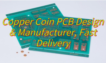
What is copper coin PCB? Let’s explore its benefits, applications, technical spec, cost reduction solution, production process and market analysis for copper coin PCB.
Are you worried about these problems?
- Is your electronics product throttling due to inadequate heat dissipation, causing performance loss?
- Are traditional PCB cooling solutions eating into your profit margins with skyrocketing costs?
- Does complex multi-layer stacking design keep your product yield below 90%?
As a copper coin PCB manufacturer, EBest Circuit (Best Technology) can provide you service and solution:
- Embedded copper coins slash thermal resistance by 60%, run devices at full power, no derating.
- Integrated heat dissipation design eliminates extra cooling modules, cutting total costs by 25%.
- Standardized copper coin insertion process boosts yield to 95% and shortens lead time by 30%.
Welcome to contact us if you have any request for copper coin PCB design and manufacturing: sales@bestpcbs.com.
What Is Copper Coin PCB?
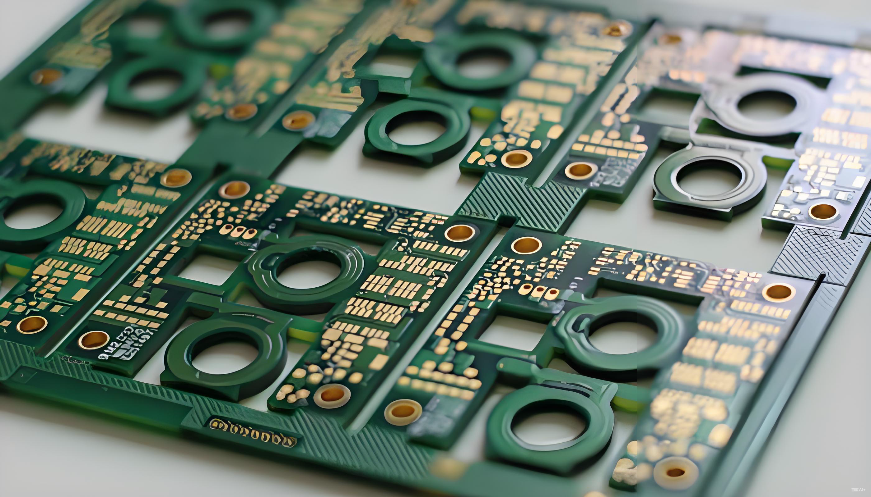
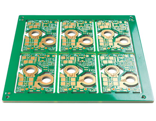
Copper Coin PCB is a specialized design that embeds solid copper blocks (copper coins) into multi-layer printed circuit boards. These copper coins directly connect heat-generating components to external heat sinks, creating high-efficiency thermal paths. Features include copper coin placement under high-power devices (in shapes like circles, rectangles, or stepped designs) to maximize contact area, boosting thermal dissipation efficiency by up to 55x compared to traditional methods like thermal vias or heat sinks.
Advantages of PCB Copper Coin
Benefits of copper coin PCB:
- High Thermal Conductivity: Copper’s excellent heat dissipation properties rapidly transfer heat away from components, reducing device operating temperatures and enhancing stability and longevity.
- High Current Carrying Capacity: Thick copper layers or coin-shaped structures enable higher current handling, minimizing resistive losses for high-power applications.
- Enhanced Mechanical Durability: Copper coin designs strengthen PCB resistance to vibration and impact, reducing physical damage risks during transport or use.
- Cost Efficiency: Optimized copper layout reduces precious metal usage or replaces external heat sinks, lowering overall manufacturing costs.
- Improved Reliability: Reduced thermal stress minimizes component failures, lowering post-sale maintenance costs and extending product lifecycle.
- Simplified Design Process: Integrated heat dissipation and current pathways eliminate the need for external cooling modules, shortening development cycles and streamlining assembly.
Applications of Copper Coin- Embedded PCB
- Aerospace & Space Exploration: Core modules of onboard computers in satellites, Mars rovers, and other space equipment.
- 5G Base Stations & RF Modules: Power amplifiers (PA) and RF front-end modules in 5G base stations.
- Electric Vehicles & Power Control: Motor controllers, battery management systems (BMS), and IGBT modules in electric vehicles.
- High-Performance Computing & Servers: High-performance computing (HPC) modules, GPU accelerators, and CPU/GPU thermal management modules in data centers.
- Industrial Control & Frequency Converters: Industrial PLCs, frequency inverters, and variable-frequency drives.
- Miniature Medical & Wearable Devices: Cardiac pacemakers, implantable medical devices, smartwatches, and other compact electronic devices.
Copper Coin PCB Technical Specifications
| Parameter Category | Detailed Specifications |
| Substrate Material | FR4 (Tg170), Rogers RO4350B, Aluminum-composite |
| Copper Layer Thickness | 1-10 oz (35-350μm) |
| Copper Coin Structure | Diameter 0.3-10mm, Height 0.2-5mm, embeddable in single/multilayer PCB |
| Thermal Performance | Thermal conductivity ≥380W/mK (pure Cu), ΔT ≤20°C@100W |
| Electrical Performance | Impedance control ±10%, insertion loss ≤0.5dB@10GHz |
| Mechanical Strength | Vibration resistance: IEC 61373, shock ≥50G |
| Manufacturing Process | Min trace/space 0.1mm, min laser drill diameter 0.1mm |
| Temperature Range | Operating: -55°C~150°C, Storage: -65°C~170°C |
| Surface Finish | ENIG, OSP, HASL |
| Reliability Testing | Compliance with AEC-Q200, MIL-STD-883 standards |
How to Design Copper Coin PCB to Reduce Production Cost?
1. Streamlined Layer Architecture
- Design Principle: Minimize layer count (e.g., 2-layer vs. multi-layer) to reduce material costs (FR-4 substrate) and simplify lamination/drilling.
- Cost Impact: 4-layer boards cost 30–50% more than 2-layer equivalents.
- DFM Alignment: Collaborate with manufacturers to optimize panel layout (e.g., 18×24 inch standard panels) for 10–20% less material waste.
2. Standardized Material & Copper Coin Integration
- Material Selection: Use cost-effective FR-4 for general applications; avoid high-frequency/specialty substrates unless required.
- Copper Thickness: Optimize for 1 oz (35µm) instead of 2 oz+ to reduce copper usage unless high current is critical.
- Coin Embedding: Pre-shape standard copper coins to avoid custom machining; embed via pre-milled grooves for flat alignment during lamination.
3. Optimized Drilling & Via Design
- Via Standardization: Use ≥0.4mm drill sizes for cost efficiency; avoid filled/buried vias unless necessary.
- Via Reduction: Consolidate ground/power planes to minimize via count and drilling time.
- Hole Quality: Ensure smooth hole walls via deburring to reduce rework costs.
4. DFM-Driven Layout & Trace Design
- Trace Parameters: Maintain ≥8mil line width/spacing to avoid precision etching costs.
- Grid-Based Layout: Minimize signal path lengths and copper area to reduce material usage.
- Thermal Management: Place heat-generating components on embedded copper coins for passive cooling, reducing heat sink costs.
5. Cost-Effective Surface Finishes
- OSP/HASL Preference: Choose OSP for short-term storage or HASL for budget-friendly solderability over ENIG/gold plating.
- Gold Finger Exception: Use thick gold plating (>30μin) only for high-wear contacts (e.g., gold fingers).
6. Component & Assembly Efficiency
- Component Standardization: Use common footprints (through-hole/SMT) to reduce assembly complexity.
- Placement Optimization: Group high-speed components to minimize trace lengths and EMI risks, lowering testing costs.
7. Avoid Over-Engineering
- Simplified Outlines: Use standard rectangles/circles instead of complex shapes to avoid routing/sawing complications.
- Dynamic Compensation: Pre-press alignment grooves for copper coins ensure flatness, avoiding post-lamination rework.
8. Early DFM Integration
- Design Rule Checks: Use tools like Cadence DRC/DFM to flag costly errors (acid traps, starved thermals) pre-fabrication.
- Manufacturer Collaboration: Validate design choices with fabricators to align with their capabilities and cost structures.
Copper Coin PCB Production Process
1. Copper Coin PCB Production Process
- Operations: Cutting large-size copper-clad laminate into production panels, edge grinding, rounding, washing, and baking (dry treatment).
- Parameters: Edge reserved 8-15mm for process margin; dimensions adjusted for equipment compatibility (e.g., 3×3 matrix panels from 41×49 inch sheets).
2. Inner Layer Circuit Production
- Pre-treatment: Brush/sandblast to remove copper oxidation and oil, enhancing adhesion.
- Photoresist Application: Coat liquid/dry film, cure at 80°C.
- Exposure & Development: Transfer pattern via UV exposure, develop with Na₂CO₃ to expose copper for etching.
- Etching & Stripping: Acidic etchant (CuCl₂) removes unprotected copper; NaOH strips cured film.
- AOI Inspection: Optical detection of shorts, opens, and defects.
3. Lamination
- Brown Oxidation: Create rough organic-metal layer on inner copper for interlayer adhesion.
- Stacking & Pressing: Layer inner boards, prepreg (PP sheets), and copper foil; vacuum hot-press at ~180°C, 350psi.
- Post-treatment: Cooling press, trimming excess resin for uniform thickness.
4. Drilling
- Positioning & Drilling: X-ray locates holes; high-speed drill (150k RPM) creates via holes (down to 100μm).
- Deburring: Remove burrs and residue for smooth hole walls.
5. Hole Metallization & Plating
- Chemical Copper Deposition: Deposit 1μm copper on hole walls/board surface.
- Electroplating: Thicken copper to 20-25μm; outer layers coated with tin for protection.
6. Outer Layer Circuit Production
- Process: Similar to inner layers but uses positive film process: tin-plating protects circuits, etching removes excess copper, then tin stripped.
- Parameters: Line width/spacing meets design specs (e.g., min 6mil), avoiding film residue/shorts.
7. Solder Mask & Silkscreen
- Solder Mask: Apply green ink; expose/develop to expose pads/holes (20-30μm thickness).
- Silkscreen: Print text/symbols; UV-cured for permanent marking.
8. Surface Finish
- Common Processes: HASL (spray tin), ENIG (chemical gold), OSP, or electroplated nickel-gold.
- Special Applications: Gold fingers require >30μin thick gold for durability.
9. Profiling
- Cutting Methods: CNC milling, stamping, laser cutting, or V-cut (for easy breakaway).
- Precision: Edge smoothness, ±0.1mm tolerance, chamfered edges to prevent stress.
10. Electrical Testing
- Methods: Flying probe or dedicated testers for continuity, impedance, and short/open checks.
11. Final Inspection & Packaging
- Inspection: Visual/AOI checks for defects (scratches, exposure), dimensional accuracy, hole tolerance.
- Packaging: Cleaned, dried, vacuum-packed/moisture-barrier bags with inspection reports and labels.
Copper Coin PCB Market Trends Analysis in 2025
Accelerated Technology Standardization
- IPC will release the IPC-7095D standard in Q2 2025, specifying embedded copper coin tolerances (±0.05mm) and thermal cycling test protocols.
- Industry yield rate rises from 85% (2023) to 92%, reducing SMEs’ design cycles by 30%.
NEV Emerges as Primary Growth Market
- Global EV production will hit 28 million units (DIGITIMES 2024), with >52% adoption of SiC MOSFETs in powertrains (operating >150℃).
- Automotive-grade Copper Coin PCB demand surges 40%, priced 3.8× higher than standard FR-4 PCBs.
Hybrid Substrate Solutions Gain Traction
- Copper-Aluminum Nitride (AlN) substrates achieve 650W/m·K thermal conductivity (96% CTE match), with costs dropping 25% due to mass production.
- Penetration in data center GPU thermal modules reaches 38% (vs. 12% in 2023).
Regional Supply Chain Restructuring
- North American players (TTM/Ventec) dominate aerospace (55% share), but China’s “New Infrastructure” policy boosts local players like SCC (share up from 19% to 28%).
- Geopolitical tensions drive copper raw material price volatility (±18%).
Environmental Regulations Drive Tech Innovation
- Revised EU WEEE Directive (2025) mandates ≥90% PCB copper recovery, increasing chemical etching waste treatment costs to $85/ton.
- Laser etching investments grow 200%, reducing copper waste by 12%.
Why Choose EBest Circuit (Best Technology) as Copper Coin PCB Manufacturer?
Reasons why choose us as copper coin PCB manufacturer:
19 Years of Manufacturing Expertise
- 19 years of expertise in Copper Coin PCB manufacturing, mastering end-to-end core technologies from design to mass production.
- Thermal management efficiency improved by 50%, product reliability increased by 30%, meeting high-demand scenarios such as aerospace and 5G.
24-Hour Rapid Prototyping Capability
- Laser drilling + automated SMT lines enable sample delivery within 24 hours, supporting design iteration validation.
- Saved 2 weeks of development time for smart wearable projects, seizing market opportunities.
Complimentary DFM Design for Manufacturability
- Optimizes trace width/spacing and hole tolerance during design phase to avoid solder mask bridge risks.
- Provides standardized Gerber file checks, reducing design errors by 40% and improving production efficiency by 20%.
Integrated PCBA Solutions
- Integrates full-process solutions including PCB manufacturing, SMT placement, DIP insertion, programming testing, and burn-in testing.
- Supports ISO 13485/IATF 16949 certifications, reducing supply chain costs by 15%-25% through process simplification.
Advanced Embedded Copper Coin Technology
- Adopts 3.0×3.0mm to 60×80mm stepped copper coins with thermal conductivity 30-200 times higher than conventional materials.
- Enhances heat dissipation efficiency by 50%, reduces power module temperature by 30%, suitable for new energy vehicles and IGBT modules.
Flexible Order Processing & Fast Delivery
- Supports orders from small batches to large volumes, with 4-layer PCB designs replacing 6-layer structures to improve material utilization by 30%.
- Shortens lead time to 3-5 days, increases emergency order response speed by 40%.
Professional Engineering Support
- Circuit design engineers + process engineers execute 8D problem-solving processes.
- First-article verification + hourly patrol checks + final-article comparison, improving production yield to 98%.
High Reliability Testing & Validation
- 100% flying probe testing, thermal stress testing (288°C solder furnace reflow x3), and humidity aging (85°C/85%RH for 168 hours).
- Extends product lifespan, reduces failure rates, and enhances trustworthiness.
Welcome to contact us if you have any request for copper coin PCB: sales@bestpcbs.com.