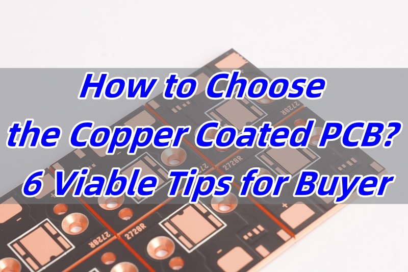
What is copper coated PCB board? Let’s explore its meaning, benefits, applications, design guide and consideration, production process through this blog.
Are you worried about these problems?
- Copper Oxidation in Standard PCBs: How to ensure long-term conductivity stability?
- High-Frequency Signal Loss: How to enhance copper foil adhesion and reduce impedance?
- High Cost for Small-Batch Customization: Can cost-effectiveness and fast delivery coexist?
As a copper coated PCB manufacturer, EBest Circuit (Best Technology) can provide service and solutions:
- Anti-Oxidation Copper Coating: Nano-scale sealing process improves oxidation resistance by 300%, with conductivity decay <2% over 5 years.
- Dynamic Lamination Technology: Gradient temperature control achieves 1.5N/mm² copper-to-substrate adhesion, reducing high-frequency signal loss by 40%.
- Flexible Supply Chain: 24 hours rapid prototyping + tiered pricing model; minimum order quantity reduced by 60% to 10㎡ compared with industry standard.
Welcome to contact us if you have any request for copper coated PCB board: sales@bestpcbs.com.
What is Copper Coated PCB Board?
A Copper Coated PCB Board is a printed circuit board where a uniform copper layer, typically 17 to 105 micrometers thick, is applied to the surface of an insulating substrate. This copper layer forms conductive pathways for transmitting electronic signals, distributing power, and dissipating heat. Manufactured through precision processes like etching, drilling, and plating, the copper adheres firmly to the substrate, ensuring high electrical conductivity, thermal conductivity, and mechanical strength.
What Are Advantages of Copper Coated PCB?
- High-fidelity signal transmission: Ultra-high electrical conductivity minimizes signal attenuation, enabling precise signal routing in high-frequency/high-speed designs while reducing EMI and crosstalk.
- Enhanced thermal management efficiency: High thermal conductivity (380-401 W/(m·K)) achieves efficient heat dissipation without requiring additional cooling modules, extending device lifespan and mitigating thermal failure risks.
- Robust mechanical reliability: Strong peel strength (≥1.4 N/cm) ensures secure bonding between copper layers and substrates, withstanding harsh environmental stresses like industrial vibration and automotive impacts.
- Expanded design freedom: Supports fine-line processes (line width/spacing ≤50μm) to meet miniaturization demands in consumer electronics and 5G devices, enabling higher routing density and space utilization.
- Optimized cost efficiency: Copper’s cost advantage (1/100 of silver, 1/1000 of gold) combined with mature plating/etching processes balances BOM costs while ensuring stable mass production supply.
- Broad process compatibility: Adapts to diverse substrates (FR-4, ceramic, metal-based) and surface treatments (OSP/ENIG), compatible with lead-free soldering and seamless multi-scenario application.
- Strengthened EMI shielding: Natural copper shielding effect reduces external interference, ideal for sensitive equipment like medical and aerospace systems requiring ultra-stable signal performance.
- Outstanding environmental compliance: Meets RoHS/REACH standards with >95% copper recovery rate, lowering waste disposal costs and enhancing sustainability credentials.
What Are Applications of Copper Coated PCB Board?
- 5G base station antenna board
- Data center server backplane
- Electric vehicle inverter module
- Supercharging pile power distribution board
- Deep space probe control board
- Downhole high-temperature sensing circuit
- Hydrogen fuel cell stack bipolar plate
- Solid-state battery lithium metal deposition substrate
Copper Coated PCB Board Design Technical Parameter
| Parameter | Specifications |
| Copper foil thickness | 0.5-3 oz (17-105μm) |
| Conductivity | 58.6×10⁶ S/m |
| Thermal conductivity | 380-401 W/(m·K) |
| CTE (Coefficient of Thermal Expansion) | 17 ppm/℃ |
| Peel strength | ≥1.4 N/cm |
| Dielectric constant | 4.5-4.8 |
| Dielectric loss | Low (e.g., 0.01) |
| Water absorption | ≤0.1% |
| Flame retardancy | UL94-V0 |
| Surface roughness | ≤1.6 μm |
| Copper purity | ≥99.9% |
| Current carrying capacity | 1A/0.5-1mm line width |
| Thermal decomposition temperature | ≥340 ℃ |
How to Design Copper Coated PCB to Reduce Production Cost?
Methods about how to reduce production cost through copper coated PCB board design:
1. Precise Copper Thickness Selection
- Match copper thickness to actual current needs: use 0.5oz (18μm) for RF circuits ≤3A/mm² and 2oz (70μm) for high-temperature zones like automotive ECUs. Localized thickening saves 20-30% copper costs while maintaining conductivity.
2. Cost-Effective Surface Finishes
- Choose between low-cost HASL (100-500μm, 40-60% cheaper than ENIG) for consumer electronics and high-performance ENIG (2-6μm gold, 99.9% purity) for 5G/high-frequency areas.
3. Layout Optimization for Material Efficiency
- Achieve ≥85% material utilization through compact routing. Replace 90° traces with 45° angles to reduce etching defects and signal loss. Use buried vias instead of through-holes to cut drilling costs by 30%.
4. DFM Rules for Manufacturing Yield
- Standardize trace width/spacing ≥50μm for conventional processes and ≥30μm for HDI. Enforce 3W rule (minimum spacing ≥3× line width) to prevent shorts, reducing defect rates by 50%. Avoid sharp angles ≥90° to minimize etching errors.
5. Balanced Substrate and Layer Count
- Use FR-4 for digital circuits ($0.5/㎡) and high-speed materials like FR-408 only where necessary. Reduce layer count from 6 to 4 layers through optimized ground plane partitioning, saving 25% lamination costs while maintaining signal integrity.
6. Panelization and Process Scaling
- Maximize panel utilization to ≥90% using V-cut or tab routing. For small boards, adopt 2×2/3×3 matrix paneling to reduce per-unit costs by 10-15%. Source locally to cut logistics costs by 20%.
7. Targeted Testing and Validation
- Use flying probe testing for small batches, saving 30% on fixtures. Limit impedance testing to high-frequency zones. Pre-validate designs with tools like Altium/Cadence to reduce prototype iterations and rework costs by 40%.
8. Standardization and Modular Design
- Build libraries of standard footprints and routing rules to cut design time by 30%. Reuse modules (power/interface blocks) to reduce NRE costs by 25%. Collaborate with manufacturers on process parameters like etch times and lamination temperatures.
How to Make Copper Coated on PCB Board?
1. Pre-Cleaning & Surface Preparation
- Deburring: Remove drilling residues/mechanical burrs using abrasive brushes or chemical agents.
- Alkaline Degreasing: Immerse PCB in alkaline solution (e.g., NaOH) to eliminate oils, fingerprints, and oxides.
- Desmear: Apply potassium permanganate (KMnO₄) to etch epoxy resin residues from hole walls, enhancing surface adhesion.
- Micro-Etching: Use sulfuric acid/hydrogen peroxide (H₂SO₄ + H₂O₂) to create micro-roughness (5-15μin Ra) for optimal copper adhesion.
2. Electroless Copper Plating (Seed Layer)
- Activation: Coat hole walls/PCB surface with palladium (Pd) catalyst via immersion in Pd-Sn colloid solution.
- Chemical Bath: Submerge PCB in alkaline copper bath (CuSO₄ + formaldehyde/reducing agent) at 50-70°C for 15-30 min.
- Deposition: A uniform 0.2-0.8μm copper layer forms through redox reaction, enabling electrical conductivity for through-holes.
3. Electrolytic Copper Plating (Thickness Enhancement)
- Electroplating Setup: Connect PCB as cathode in copper sulfate (CuSO₄) bath with phosphorized copper anodes.
- Current Control: Apply DC current (1-3 A/dm²) for 30-60 min to achieve target thickness (15-35μm).
- Additives: Use brighteners/levelers to ensure uniform coating and prevent pitting.
4. Patterning & Etching
- Photoresist Application: Coat PCB with photoresist, expose to UV through circuit mask, and develop to expose non-conductive areas.
- Etching: Submerge in ferric chloride (FeCl₃) or ammonium persulfate bath to remove excess copper, leaving conductive traces.
- Resist Stripping: Remove remaining photoresist with NaOH solution to reveal final copper circuitry.
5. Post-Treatment & Protection
- Oxidation Prevention: Apply organic solderability preservative (OSP) or immersion gold (ENIG) to protect copper from oxidation.
- Laminate Bonding: For multilayer PCBs, laminate copper-plated layers with prepreg under heat/pressure (180-200°C, 300-500 psi).
- Quality Inspection: Conduct automated optical inspection (AOI) to verify trace integrity and hole plating uniformity.
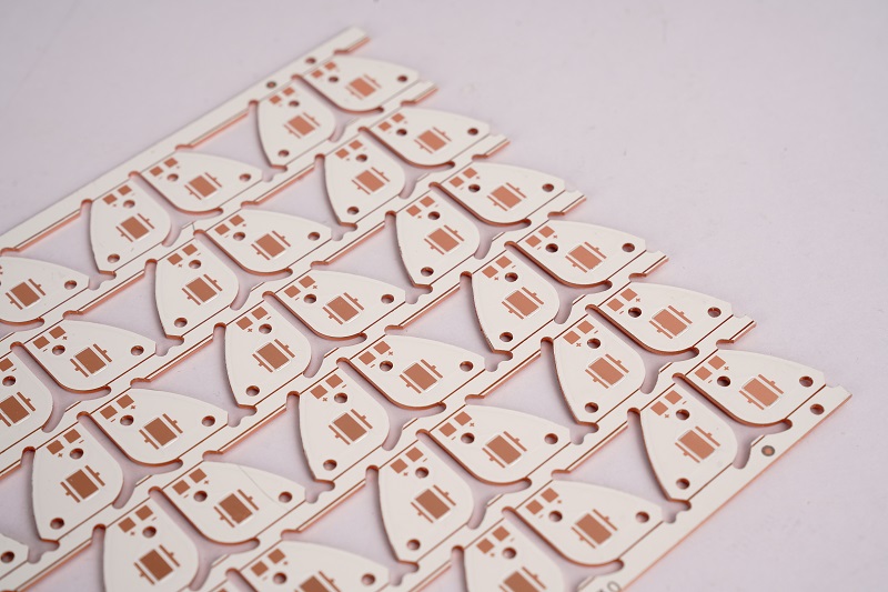
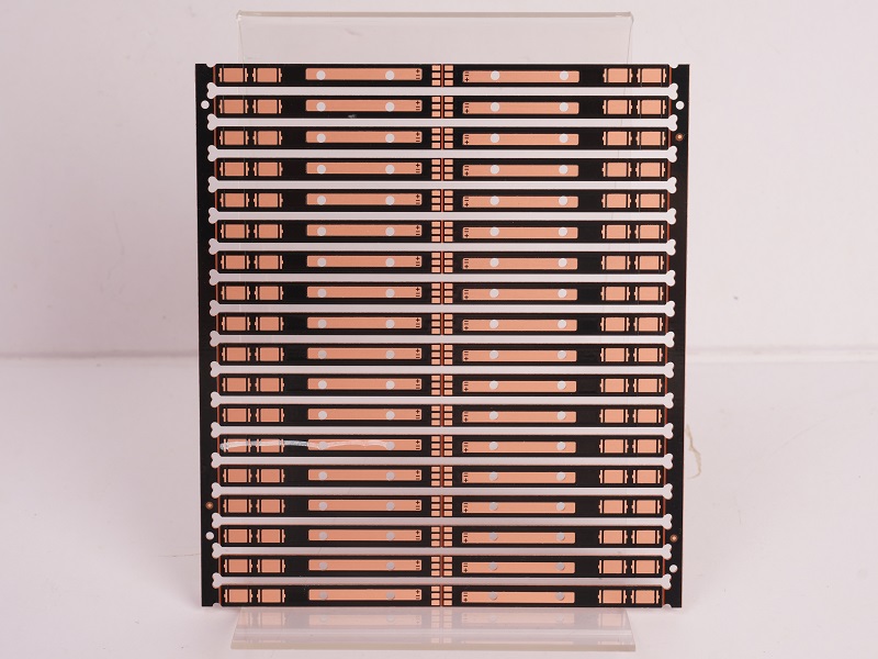
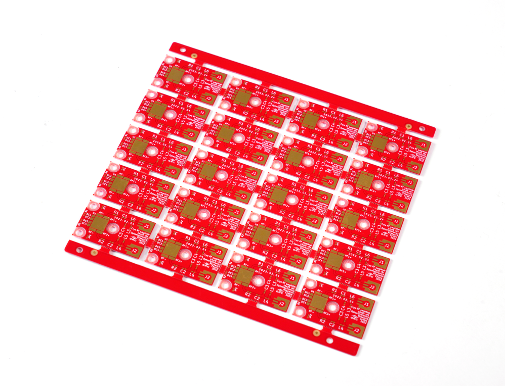
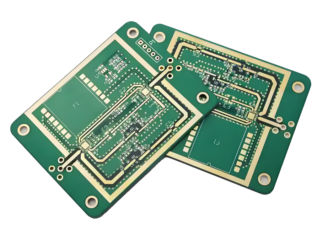
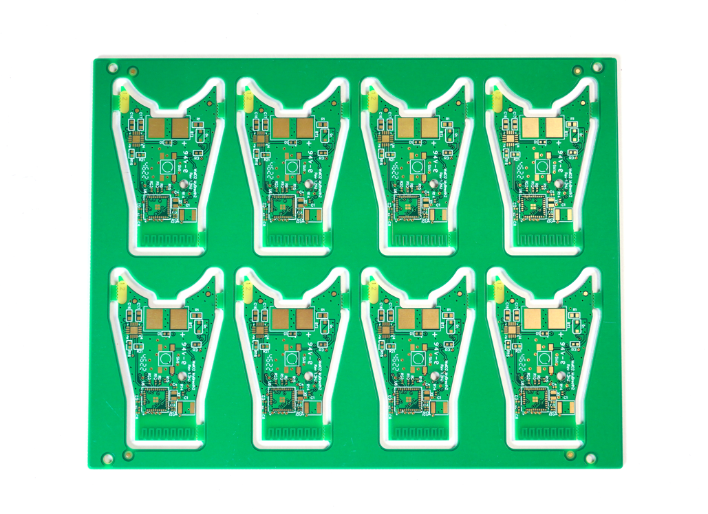
Our Copper Coated Printed Circuit Board Case Studies
Below is a photo of copper coated PCB board we made before:
| Product Name: | Copper Coated PCB |
| Material: | Copper-clad laminate |
| Quality Standard: | IPC6012 Class II/III |
| IPC6012 Class II/III | 2.5-4.0 |
| Layers: | 2-34 layers |
| Thickness: | 0.1mm-12mm |
| Copper Thickness: | Base copper 0.5-3oz (17-105μm); finished copper 1-4oz (35-140μm) |
| Surface Finishes: | ENIG, OSP, HASL etc. |
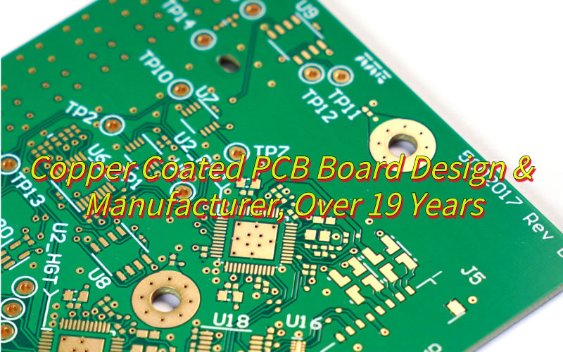
Why Choose EBest Circuit (Best Technology) as Copper Coated PCB board Manufacturer?
Reasons why choose us as copper coated PCB board manufacturer:
- 19-Year Copper Plating Expertise: Leveraging 19 years of specialized copper plating technology, we achieve 0.2mm fine-line processing and ±10% hole copper thickness uniformity control, reducing rework costs caused by process defects.
- Customized Multi-Type Copper Plating: Offering chemical plating, electroplating, pulse plating, and other processes tailored to scenarios like EV chargers and solar inverters, enhancing product performance compatibility.
- 24-Hour Rapid Prototyping: Utilizing MES intelligent systems and local supply chains to deliver prototypes within 24 hours, accelerating R&D cycles and market entry.
- Transparent Full-Process Quality Control: Adhering to IPC Class 2 standards with 36 inspection steps (including X-ray copper thickness testing and 100A load aging tests), ensuring batch-level quality traceability and stable delivery performance.
- 100% Batch Inspection Guarantee: Implementing full-batch inspection with SPC statistical control and 8D problem-solving, preventing bulk defects and minimizing after-sales risks.
- Thick Copper Foil Thermal Optimization: Using ≥2oz thick copper foil and 8W/(m·K) thermal conductivity embedded blocks to cut DC resistance by 50% and outperform industry-standard temperature rise control, ensuring reliable high-power operation.
- Multi-Layer Copper Design Flexibility: Supporting 12-layer thick copper stack-ups and stepped copper layer designs (e.g., 3oz outer/2oz inner layers) for specialized needs like BMS systems and 5G base stations, optimizing space utilization and electrical performance.
Welcome to contact us if you have any request for copper coated PCB: sales@bestpcbs.com.