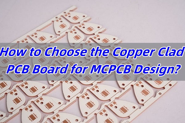
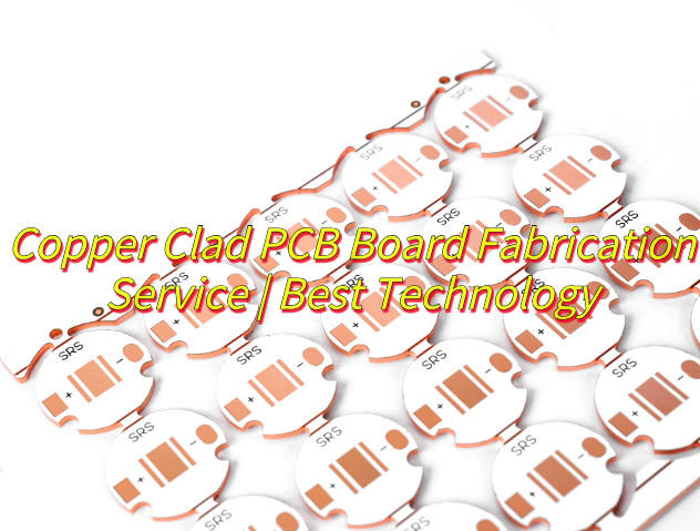
What is copper clad PCB board fabrication? Let’s discover its definition, types, applications, production process and why choose EBest Circuit (Best Technology) as copper PCB manufacturer.
Are you troubled with these problems?
- High Thermal Resistance & Poor Heat Dissipation?
- Unstable Processing Yield?
- Small-Batch Order Barriers?
As a copper clad PCB board manufacturer, EBest Circuit (Best Technology) can provide service and solutions:
- Superconducting Copper Tech: High-thermal-conductivity ceramic resin (≥5W/mK) cuts thermal resistance by 40%, doubling device lifespan.
- Full-Cycle Yield Control: Laser precision + detection ensures cost-efficient, consistent batch quality (≥96% yield).
- Rapid Custom Production: From prototypes to volume production, 10-day delivery with free DFM analysis to accelerate time-to-market.
Welcome to contact us if you have any request for copper clad PCB board: sales@bestpcbs.com.
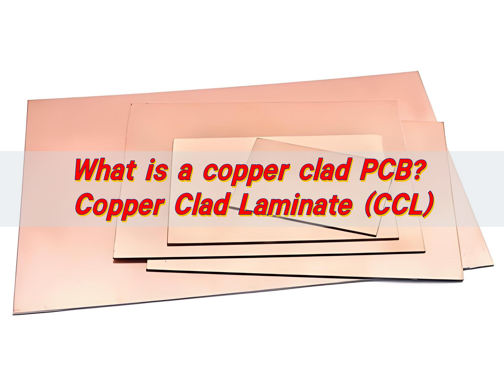
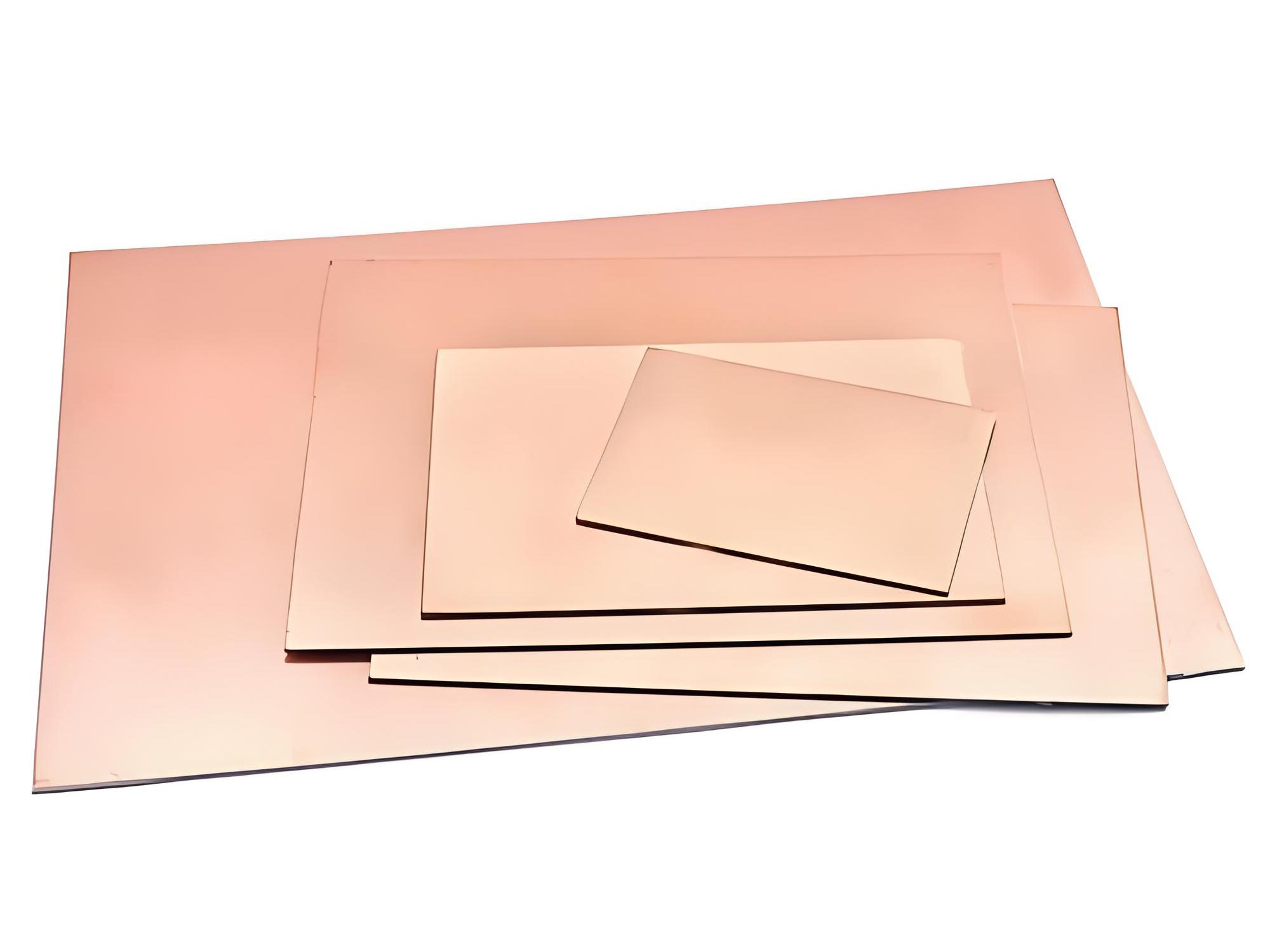
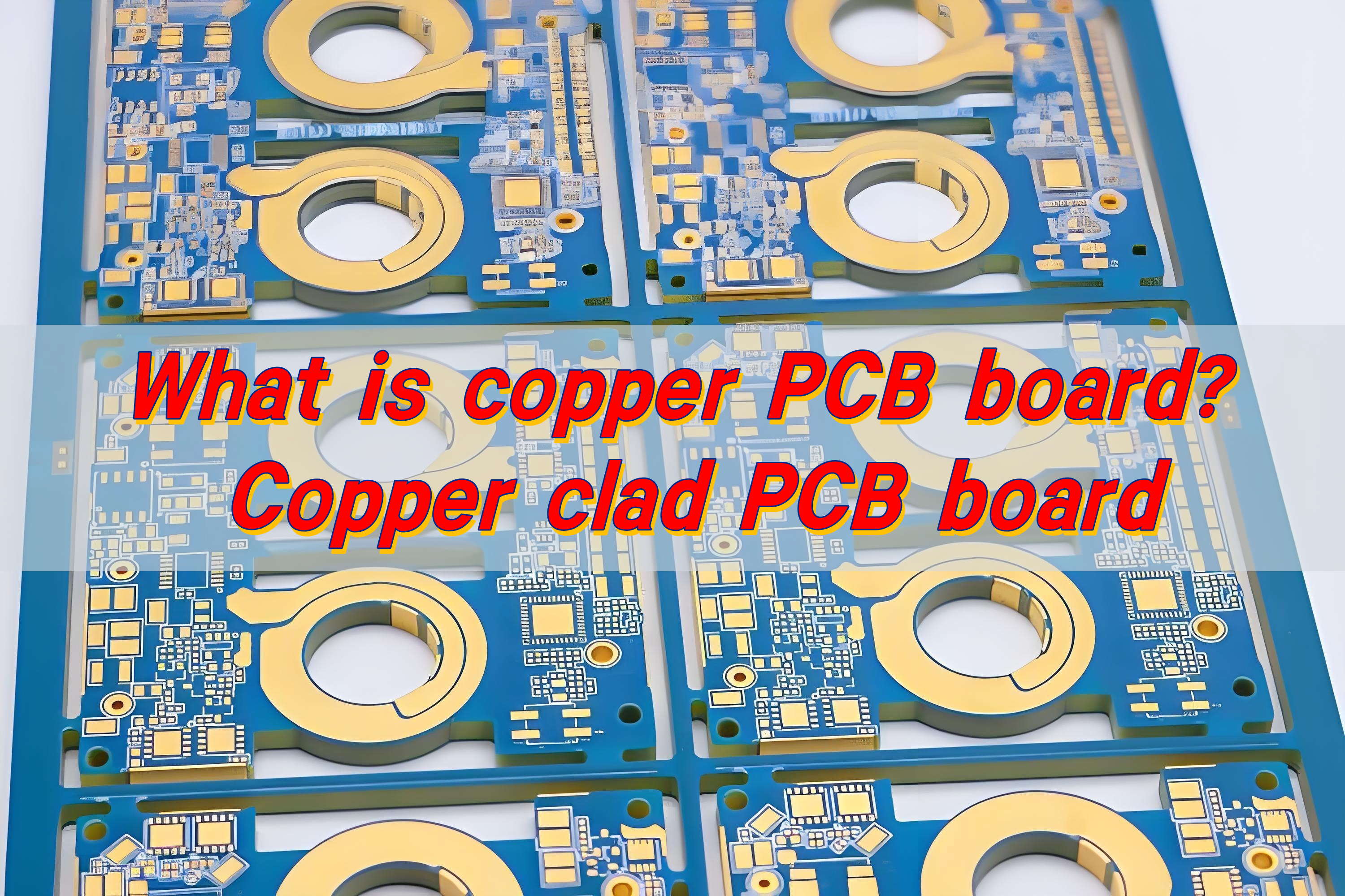
What is Copper Clad PCB Board Fabrication?
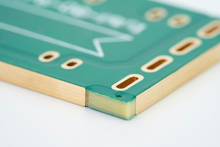
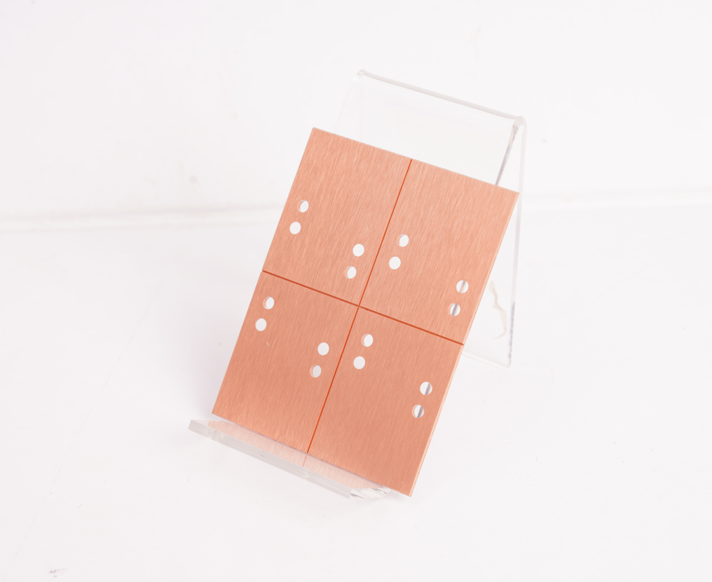
Copper Clad PCB Board Fabrication involves the process of securely coating an insulating substrate (such as epoxy resin) with a copper foil layer through a specific process, followed by precise etching to form conductive circuit patterns. This process leverages copper’s excellent electrical and thermal conductivity to provide a reliable physical carrier for signal transmission and heat dissipation in electronic devices.
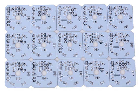
Common Types of Copper PCB Fabrication
Single-layer Copper PCB
- Single-sided copper conductive layer formed through a single etching process.
- Cost-effective and simple, suitable for low-power, low-complexity applications such as household appliance control boards, LED lighting drivers, and basic sensor circuits.
Double-layer Copper PCB
- Dual-sided copper layers with interlayer connectivity achieved via drilled-and-plated through-holes.
- Ideal for moderately complex electronics like mobile chargers, small motor drives, and industrial controllers, enabling flexible routing and component placement.
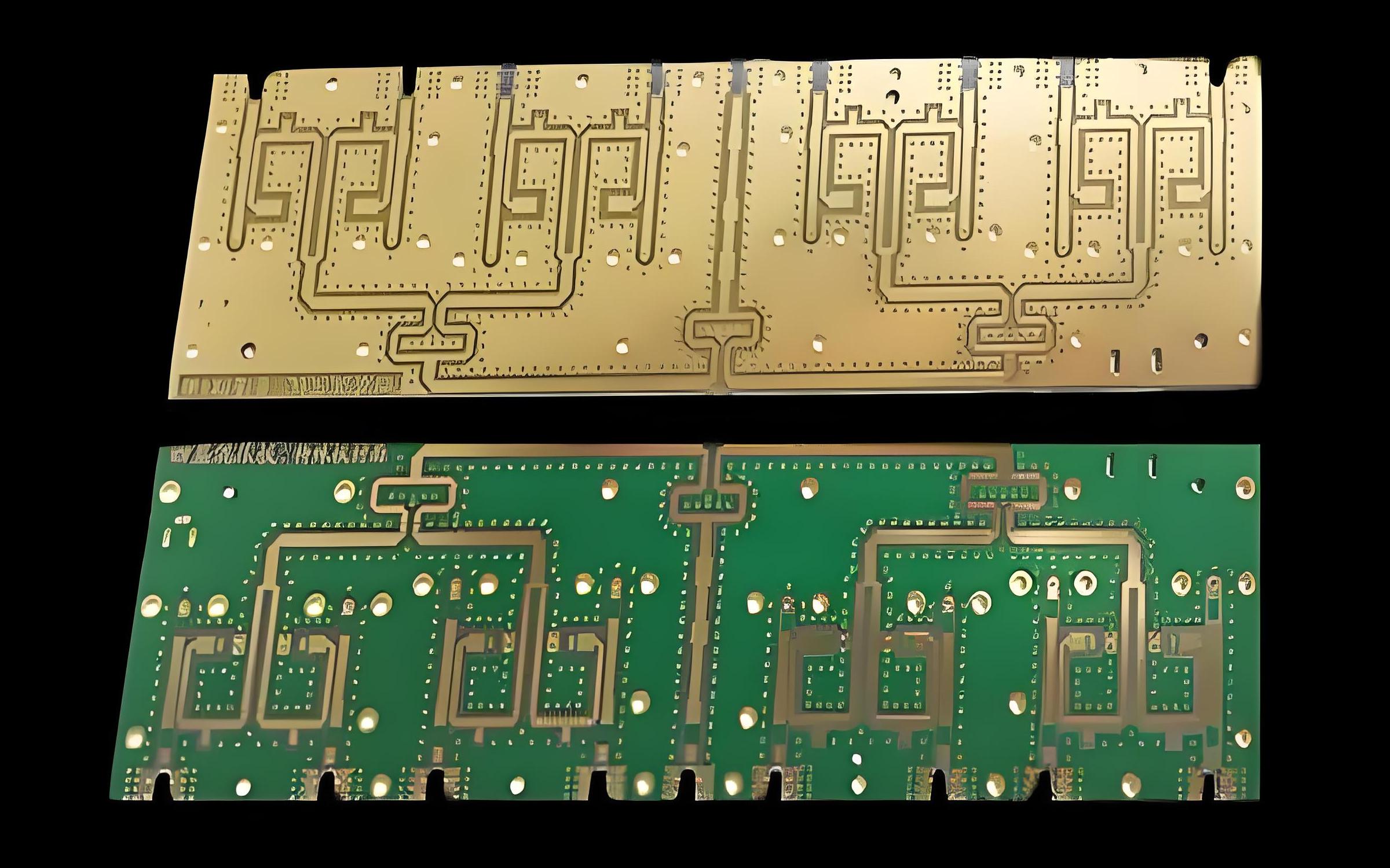
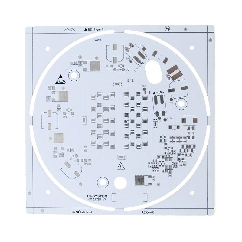
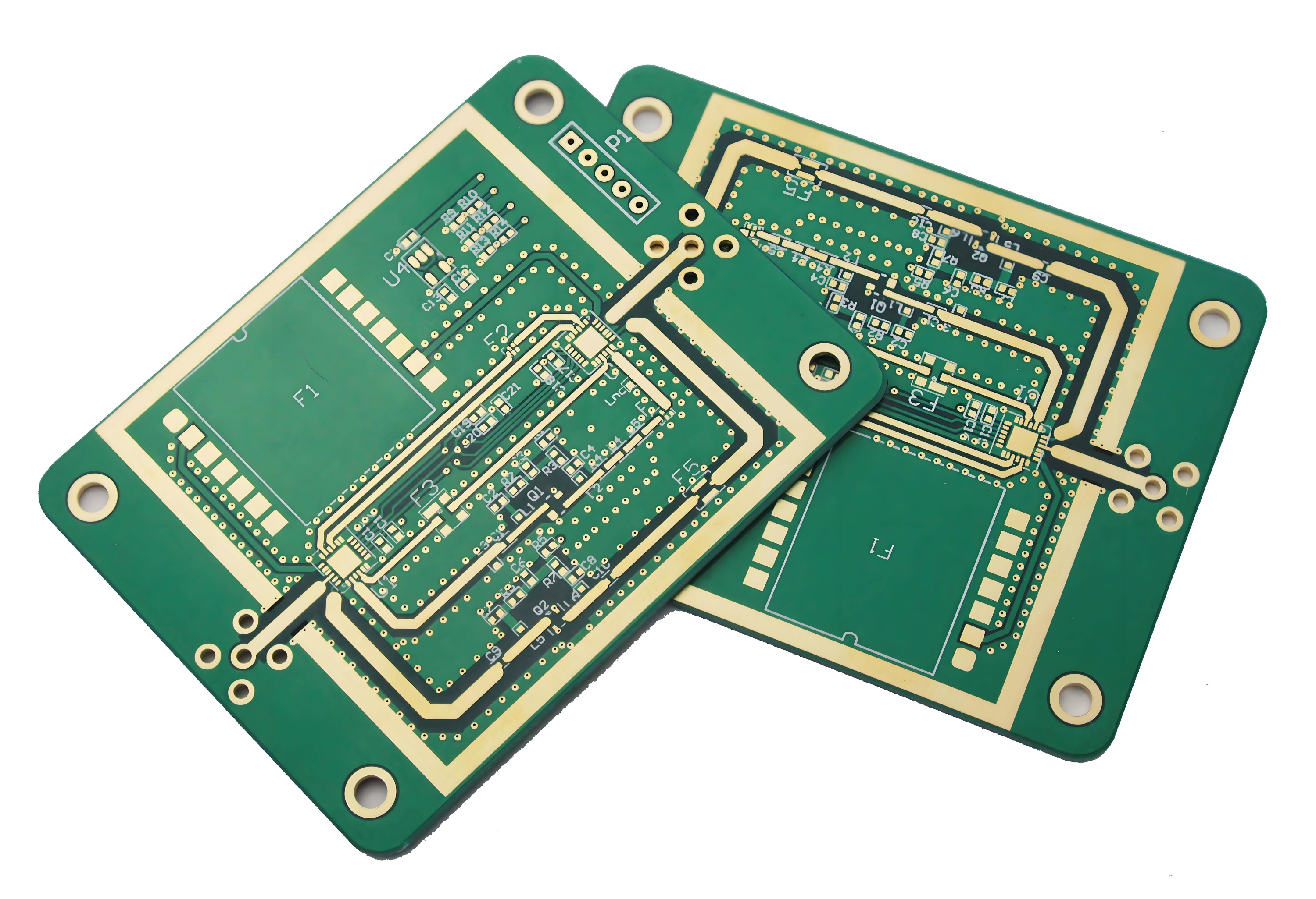
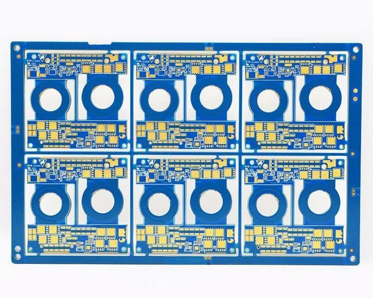
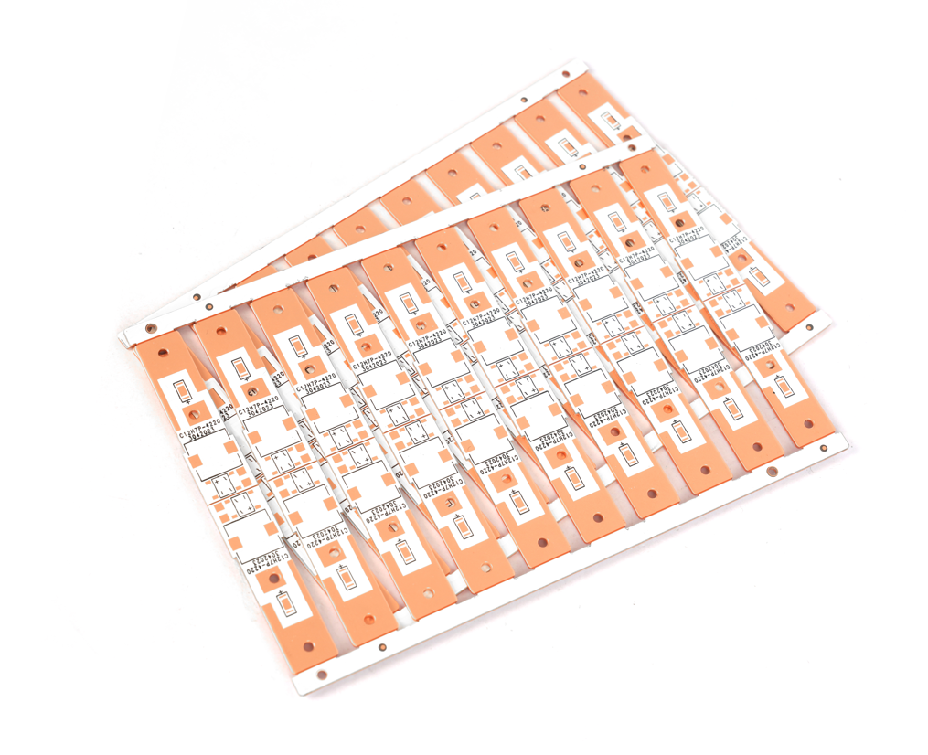
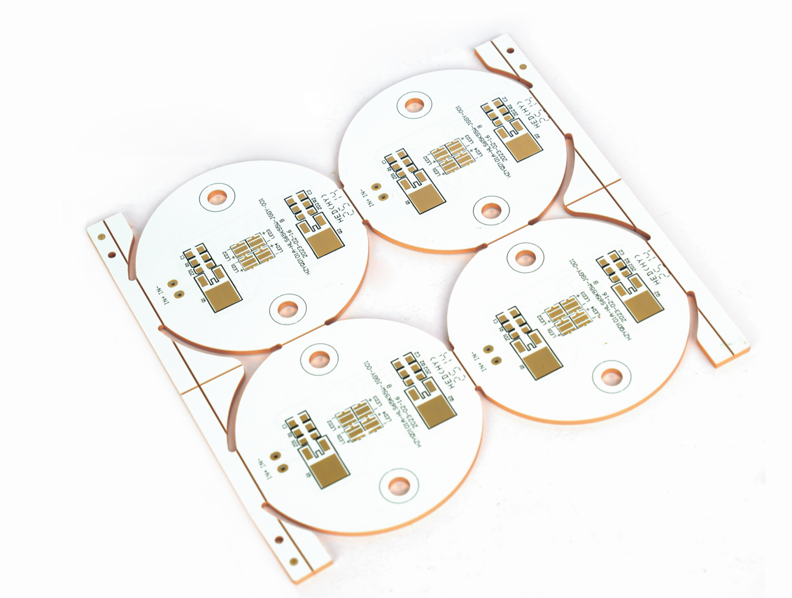
Multilayer Copper PCB
- Three or more hidden conductive layers integrated via inner-layer patterning, interlayer insulation lamination, and via/plating processes.
- Designed for high-density, high-performance scenarios including 5G communication modules, automotive power systems, and medical imaging devices, supporting high-speed signal transmission, low EMI, and efficient thermal management.
Applications of Copper Clad PCB Board Fabrication
- 5G Base Station RF Module
- EV IGBT Power Module
- Satellite Communication Payload Board
- CT Scanner X-ray Generator Control Board
- Industrial Robot Servo Drive Board
- Smartphone Motherboard
- Photovoltaic Inverter Power Module
- High-Speed Rail Traction Control Unit
Copper Clad PCB Board Fabrication Processes
1. Raw Material Preparation & Cutting
- Precision cutting of high-Tg FR-4 substrate (Tg ≥ 170°C) and 2-10oz thick copper foil using CNC panel saws, with ±0.05mm dimensional accuracy and 20mm process margins.
- Material selection ensures optimal thermal conductivity (≥3.0W/m·K) and electrical performance for high-power applications.
2. Panel Pretreatment & Circuit Formation
- Surface cleaning via alkaline degreasing (5-8% NaOH, 40-50°C, 5-10min) and acid pickling (10-15% HCl, 25-30°C, 2-3min) to achieve <30° water contact angle, ensuring strong adhesion.
- UV photolithography forms circuit patterns with ±0.01mm line width accuracy. Electroplating (1-1.5A/dm² current density, 180-220g/L CuSO₄) achieves 15-35μm copper thickness with <10% thickness variation, optimized for low resistance and high current carrying capacity.
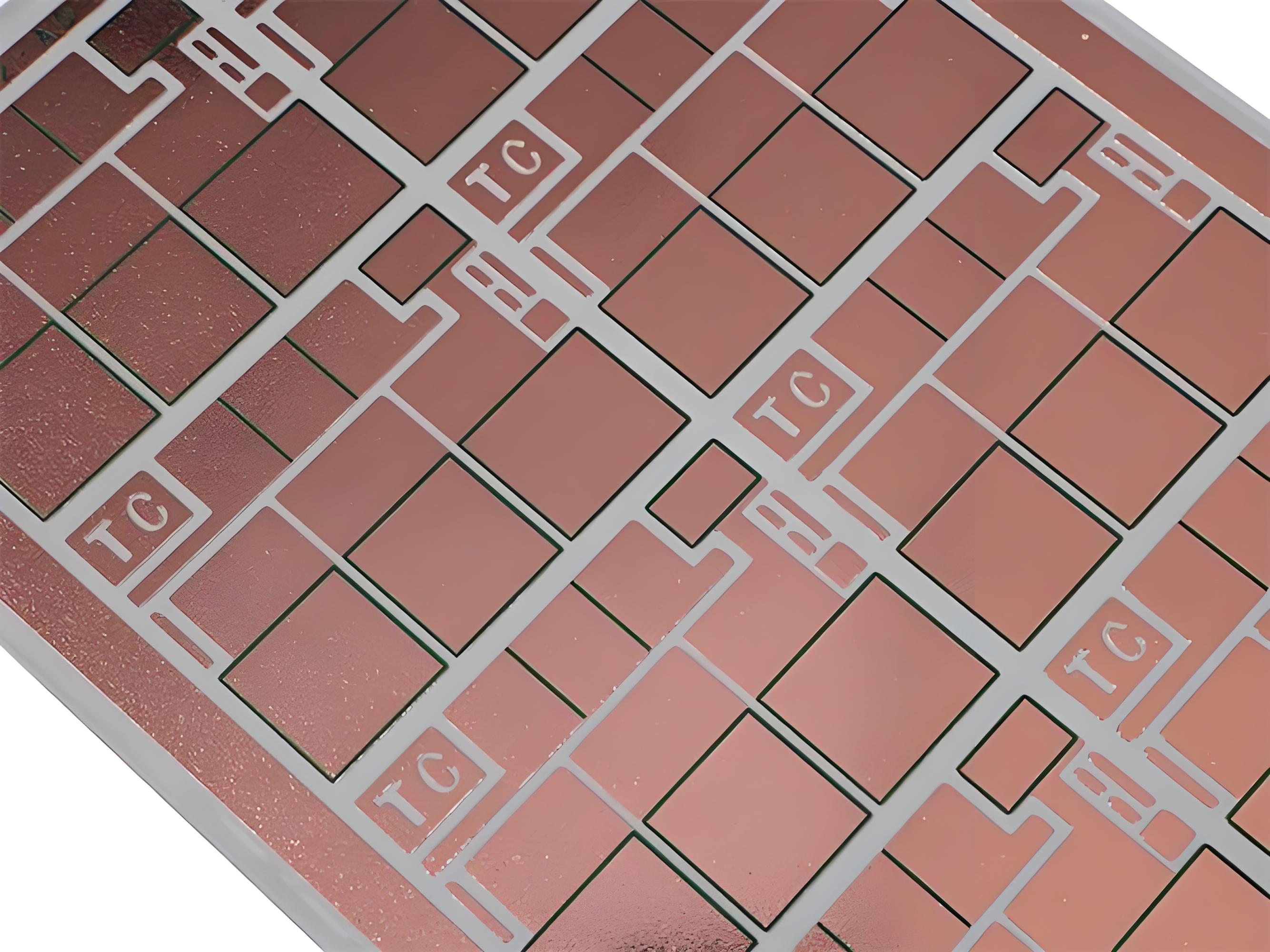
3. Circuit Quality Control & Etching
- Multi-stage QC includes visual inspection for shorts/opens, AOI for trace defects, and in-circuit testing (ICT) for electrical integrity.
- Acidic etching (FeCl₃, 38-42Be’, 45-50°C) with controlled spray pressure minimizes undercut (<10% line width). Residual copper removal ensures <0.1% residual copper rate, critical for signal integrity in high-frequency applications.
4. Substrate Preparation & Convex Platform Formation
- Substrate blanks cut to specification; dry film photoresist (25-35μm) applied if non-copper-clad. Mechanical brushing (300-400 grit) or chemical micro-etching (H₂SO₄/H₂O₂) creates 5-15μin Ra surface roughness for enhanced bonding.
- Wet film resist (20-30μm) screen-printed on designated areas, followed by selective etching to form raised copper platforms, improving thermal dissipation and electrical connectivity in power modules.
5. Lamination & Structural Integration
- Vacuum-assisted hot pressing (30-40kg/cm² pressure, 180-200°C, 60-120min) bonds panel-substrate stacks using high-Tg prepreg (Tg 170-180°C). Vacuum level ≤10Pa prevents delamination and voids, ensuring mechanical robustness.
- Post-lamination processes include resist stripping (5-8% NaOH, 50-60°C), target drilling for alignment, and secondary surface cleaning for subsequent steps.
6. Solder Mask & Surface Treatment
- UV-curable epoxy solder mask applied via curtain coating, followed by pre-bake (75-85°C, 20min), UV exposure (1200-1500mJ/cm²), and developing (1% Na₂CO₃, 25-30°C) for precise mask alignment.
- Surface finishes include OSP (0.2-0.5μm organic coating for short-term storage), ENIG (5-8μm Ni/0.05-0.1μm Au for solderability and corrosion resistance), or lead-free HASL for RoHS compliance.
7. Outline Processing & Electrical Testing
- CNC routing for precise dimensions (±0.05mm tolerance), V-cut scoring for easy breakaway, and drilling for mounting holes.
- 100% electrical testing verifies continuity, isolation, and impedance, while environmental stress tests (-40°C to 125°C thermal cycling for 1000 cycles, 500hr salt spray) ensure long-term reliability in harsh conditions.
8. Final Inspection & Packaging
- FQC visual inspection checks for surface defects, while FQA sampling validates compliance with IPC-A-600 standards.
- Vacuum-sealed packaging with desiccant and QR codes ensures traceability and protection against moisture/oxidation. Final warehouse entry and shipment follow strict quality audit protocols.
Our Copper Clad PCB Board Fabrication Capabilities
| Items | Technical Parameters |
| Product model | Copper Based |
| Copper trace thickness | 1OZ, 2OZ, 3OZ, 4OZ, up to 10OZ |
| Thermal Conductivity | 1.0, 1.5, 2.0, 3.0W/m.K |
| Surface finishing | HAL(LF)/ Gold Immersion/ Gold plating/ OSP/ Immersion Tin/ Silver Immersion |
| Soldermask Color | White/Black/Green/Blue/Red/Yellow |
| Layers | 1L, 2L, 4L, 6L, 8L, double sided, COB |
| Maximum dimension | 1,100mm*480mm; 1,500x300mm |
| Minimum dimension | 5mm*5mm |
| Minimum Line width/space | 0.1mm/0.1mm |
| Warp and twist rate | ≤0.75%(thickness:1.6mm, measurement:300mm×300mm) |
| Board Thickness | 0.3-4.5mm |
| Die-Punching dimension tolerance | ±0.15mm |
| V-cut positioning tolerance | ±0.1mm |
| Manufacturing capability | 6000m2 |
| Wall Cu thickness | 15-25um |
| Alignment tolerance | ±0.076mm |
| Minimum diameter of die-punching hole | Thickness <=1.0mm: 1.0mm |
| Thickness 1.2-3.0mm: 1.5mm | |
| Thickness 4.0mm: 2.0mm | |
| Minimum size the square groove/slot/cutout | Thickness <=1.0mm: 0.8mm×0.8mm |
| Thickness 1.2-3.0mm: 1.0×1.0mm | |
| Thickness 4.0mm: 1.5×1.5mm | |
| Outline Tolerance | CNC routing:±0.1mm; Die-punching:±0.15mm |
| Minimum diameter of hole | 0.3mm; not limit for maximum diameter of hole |
| Surface Finishing Thickness | gold plating:Ni 2.5-5um, Au: 0.025-0.075um |
| immersion gold: Ni 3-6um, Au: 0.025-0.1um | |
| HAL(LF): 3-30um | |
| V-cut Angle tolerance | ±5° |
| V-cut Range | 0.3mm-4.5mm |
| Smallest silkscreen height | 0.15mm |
| Smallest PAD | 0.1mm |
Copper Clad PCB Board Fabrication Services We Offered
- Material Customization Services: Offer combinations of copper foil thickness (1-4OZ), substrate types (FR4/high-frequency materials/ceramic substrates), and surface finishes (ENIG/HASL/OSP) to suit diverse needs from consumer electronics to industrial-grade equipment.
- Precision Lamination Process: Support single-layer/double-layer/multilayer board fabrication using vacuum lamination technology to achieve strong bonding between copper layers and substrates, ensuring no bubbles or delamination for high-reliability circuits.
- Microvia Processing Capabilities: Provide mechanical drilling, laser drilling, and chemical etching microvia services to achieve blind/buried via structures with a minimum hole size of 0.1mm, supporting HDI (High Density Interconnect) designs.
- Thermal Management Solutions: Thick copper layer design (≥3OZ) combined with thermal via/heat sink processes to enhance heat dissipation efficiency for power modules (e.g., IGBT/MOSFET), supporting 200A/mm² high current density applications.
- Harsh Environment Adaptation: Custom circuit designs resistant to extreme temperatures (-65°C to 150°C), corrosion (salt spray test ≥96 hours), and vibration (random vibration ≥10G), meeting demands for aerospace, rail transit, and other extreme environments.
- 24 Hours Rapid Prototyping & Low Volume Production: Support end-to-end services from prototype design to mass production, including 48-hour rapid prototyping, small-batch trial production, and large-scale automated manufacturing to meet project needs at different stages.
- Quality Testing & Certification: Include AOI (Automated Optical Inspection), flying probe testing, impedance testing, and reliability verification (e.g., thermal shock, aging tests) to ensure compliance with international standards such as IPC and RoHS.
Why Choose EBest Circuit (Best Technology) as Copper Clad PCB Manufacturer?
Reasons why choose us as copper clad PCB fabrication manufacturer:
- 19-Year Manufacturing Expertise: Leveraging 19 years of industry experience to rapidly match similar project cases, enhance complex demand response efficiency, and boost project success rates for clients.
- Automotive & Medical Certifications: Holding IATF 16949 automotive quality certification and ISO 13485 medical device certification, meeting strict compliance thresholds for high-reliability fields to facilitate client product approval.
- Full-Process Multi-Technology Compatibility: Covering single-layer to high-layer complex circuits with full-process capabilities, reducing communication costs and launch delays caused by technological limitations.
- Proprietary Database for Rapid Response: Smart database of material/process parameters enables quick optimization scheme calls during design, shortening validation cycles by 30%+ and improving first-pass yield.
- 24 Hours Rapid Prototyping Service: 24/7 prototyping response with 48-hour deliverable samples, accelerating prototype validation and market testing to seize first-mover advantages.
- Free DFM Pre-Analysis: Complimentary manufacturability assessment during design phase to pre-identify risks (e.g., trace/space defects, via reliability), minimizing mass-production modification costs.
- Transparent Pricing with No Hidden Fees: Clear itemized quotes covering full-flow costs (materials, processes, testing) to enable precise budgeting and avoid post-factum fee disputes.
- 9-Stage Rigorous Quality Control: Implementing 9 strict inspection steps from raw material intake to finished product (e.g., AOI, flying probe, thermal shock tests) to ensure batch-to-batch consistency and reliability.
- 100% Full Inspection for Mass Production: Every PCB undergoes full inspection during volume production to eliminate defective outflows, reducing client repair costs and enhancing end-user trust.
How to Get a Quote for Copper Clad PCB Board Fabrication Service?
Copper Clad PCB Board Fabrication Quote Checklist
- Layer Count: Specify single-layer/double-layer/multilayer with exact layer count and interlayer connection structure (e.g., through-hole/blind via configuration).
- Dimensions: Include length × width (mm) and minimum trace width/spacing (e.g., 0.1mm/0.1mm).
- Substrate Type: FR4/high-frequency materials/ceramic substrate (note exact model or parameters).
- Copper Foil Thickness: 1-4OZ (clarify single-sided/double-sided/inner layer thickness).
- Surface Finish: ENIG/HASL/OSP (mention selection rationale or special requirements).
- Special Processes: Blind/buried/micro vias (minimum hole size/accuracy), high-frequency optimization (impedance control value), thermal management design (thermal via/heat sink specs).
- Production Volume: Small batch (<100 pcs)/Medium batch (100-1000 pcs)/Large batch (>1000 pcs).
- Lead Time: Standard delivery (e.g., 10 working days) or urgent needs (e.g., 48-hour prototyping).
- Certification Requirements: IATF 16949/ISO 13485/RoHS (specify if certification reports are needed).
Welcome to contact us and submit your files to get a quote for copper PCB fabrication: sales@bestpcbs.com.