Selecting the rightcopper busbar manufacturers is critical for ensuring electrical system reliability and performance. High-quality copper busbar manufacturers adhere to strict material and process standards, while poor suppliers may cause energy loss, equipment failure, or project delays. This guide breaks down key factors to evaluate manufacturers and addresses common pain points in sourcing.
How to Select Reliable Copper Busbar Manufacturers?
Prioritize manufacturers with proven material quality, advanced processes, and industry certifications. Start by verifying copper purity (≥99.9% is ideal), checking customization capabilities, and confirming compliance with global standards like ASTM B187 and UL. Partnering with such manufacturers avoids mismatched specs and delivery risks.
Key Evaluation Criteria
Raw material sourcing: Ensure use of high-purity copper (C11000 ETP or C10200 OF grade)
Manufacturing equipment: CNC machining, automated bending, and precision stamping capabilities
Quality control: In-house testing for conductivity, mechanical strength, and corrosion resistance
Customer cases: Track record in EV charging, data centers, or renewable energy sectors
What Are the Core Quality Standards for Copper Busbar Manufacturers?
Top copper busbar manufacturers follow strict standards to guarantee product performance. The primary benchmark is ASTM B187/B187M, which defines dimensional, mechanical, and chemical requirements for copper busbars. Additional standards include RoHS for environmental compliance and ISO 9001 for quality management systems.
Must-Meet Standards
Standard
Key Requirements
ASTM B187
Copper purity, tensile strength, and dimensional accuracy
UL
Electrical safety and fire resistance for industrial use
RoHS
Restriction of hazardous substances in surface treatments
Why Material Purity Matters for Copper Busbar Manufacturers?
Copper purity directly impacts conductivity and durability. copper busbar manufacturers using 99.9%+ pure copper minimize energy loss (resistivity ≤1.7241 μΩ·cm) and reduce overheating risks. Low-purity copper with impurities degrades performance over time, leading to costly system failures.
Common Copper Grades for Busbars
C11000 (ETP): 99.93% pure, ideal for general industrial applications
C10200 (OF): 99.95% pure, superior conductivity for high-current scenarios
C12200 (DHP): For general-purpose applications requiring corrosion resistance
Customization Capabilities: Key Competitiveness of Copper Busbar Manufacturers
Reliable copper busbar manufacturers offer tailored solutions for unique project needs. This includes custom dimensions, shapes, surface treatments, and insulation options. Advanced manufacturers handle complex designs (e.g., laminated busbars) and adapt to tight tolerances (±0.05mm) for seamless system integration.
Customization Options
Dimensions: Custom width, thickness, and length (up to 6m)
Shapes: Bending, punching, and CNC-machined complex profiles
Insulation: Epoxy coating, heat-shrink tubing, or powder coating
Surface Treatment Options from Top Copper Busbar Manufacturers
Surface treatments protect busbars from corrosion and enhance conductivity. Leading copper busbar manufacturers provide multiple finishing options to suit different environments, from humid industrial settings to clean data centers.
Popular Surface Treatments
Tin plating: Prevents oxidation, ideal for low-voltage applications
Nickel plating: Enhances wear resistance and solderability
Powder coating: Superior corrosion protection for outdoor use
How Do Copper Busbar Manufacturers Ensure Delivery Stability?
Delivery delays disrupt project timelines. Trusted copper busbar manufacturers maintain stable supply chains, keep inventory of standard specs, and offer clear lead-time commitments (7-15 days for standard orders, 2-4 weeks for custom). They also have backup production lines to handle unexpected demand.
Supply Chain Management Tips
Choose manufacturers with global raw material sourcing channels
Verify production capacity (minimum 100 tons/month for bulk orders)
Request clear delivery contracts with penalty clauses for delays
Industry Certifications to Verify Copper Busbar Manufacturers
Certifications are proof of a manufacturer’s expertise. Reputable copper busbar manufacturers hold ISO 9001 (quality management), IATF 16949 (automotive), and UL certifications. These credentials confirm compliance with global standards and reduce sourcing risks.
Differences in Manufacturing Processes Among Copper Busbar Manufacturers
Process gaps separate high-quality and low-grade copper busbar manufacturers. Advanced facilities use automated processes for consistency, while low-cost suppliers rely on manual labor (prone to errors). Precision machining ensures tight tolerances, avoiding fitment issues in assembly.
Process Comparison
Automated vs. manual: Automated processes reduce error rates to <0.5%
Heat treatment: Annealing (O60 temper) for flexibility or hardening (H04 temper) for strength
Testing: In-line conductivity testing vs. post-production sampling
Applications of Products from Copper Busbar Manufacturers
Copper busbar manufacturers supply components for diverse industries, where high conductivity and durability are critical. Key applications include EV charging stations, data center power distribution, renewable energy systems (solar/wind), and industrial machinery.
FAQ: Common Issues About Copper Busbar Manufacturers
Below are answers to frequent questions when sourcing from copper busbar manufacturers.
Q1: How to verify copper purity from manufacturers?
Request material test reports (MTRs) showing chemical composition. Reputable manufacturers provide MTRs compliant with ASTM standards, confirming copper purity ≥99.9%.
Q2: What is the typical lead time for custom busbars?
Most manufacturers deliver custom orders in 2-4 weeks. Rush orders (1 week) are available for urgent projects, often with a 10-15% premium.
Q3: Can manufacturers handle small-batch orders?
Yes, top manufacturers accept small batches (≥5 pieces) without compromising quality. Some offer discounted rates for repeat small orders.
Q4: How to resolve surface oxidation issues?
Choose manufacturers offering anti-oxidation treatments (tin/nickel plating). Post-delivery, store busbars in dry environments and avoid direct contact with corrosive substances.
Q5: Do manufacturers provide technical support for selection?
Reliable manufacturers assign engineers to assist with selection, based on current, voltage, and environmental requirements, ensuring optimal busbar design.
Q6: What certifications are mandatory for automotive busbars?
Automotive applications require IATF 16949 certification, along with RoHS compliance and UL 94 flammability ratings for insulation.
How to Evaluate the Cost-Effectiveness of Copper Busbar Manufacturers?
Cost-effectiveness goes beyond unit price. Evaluate total ownership cost, including quality (avoiding rework), delivery (preventing delays), and after-sales support. Cheap copper busbar manufacturers may cut corners on material or testing, leading to higher long-term costs.
Global Sourcing Guide for Copper Busbar Manufacturers
When sourcing globally, prioritize copper busbar manufacturers with local service centers to reduce logistics time and costs. US manufacturers excel in custom designs, while Asian suppliers offer competitive pricing for bulk orders. Always confirm import compliance with local standards.
We provide high-quality products from trusted copper busbar manufacturers, adhering to ASTM B187 and UL standards with customizable solutions for diverse industries. If you need reliable copper busbars, place your order with us via email at sales@bestpcbs.com.
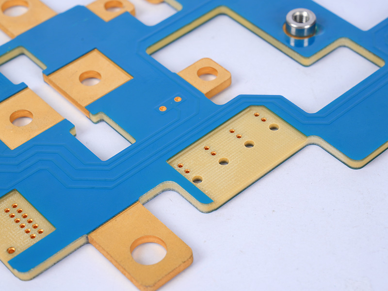
Copper busbar fabrication is the cornerstone of modern power distribution, offering reliable performance and enabling the innovative use of busbar PCBs. This blog provides a comprehensive guide to copper busbars, covering their types, sizing, ampacity, fabrication process, PCB integration, advantages, and trusted sourcing options.
Do you suffer from any of the following problems?
Design Mismatch: Many customers find that busbar dimensions, thickness, or current-carrying capacity do not perfectly align with their equipment requirements, leading to project delays or repeated redesigns.
Thermal Management Issues: In high-power applications, busbars often overheat or rise in temperature too quickly, which can compromise system stability and shorten product lifespan.
Unstable Surface Finishing: Inconsistent plating quality from some suppliers can cause oxidation on the busbar surface, increasing contact resistance and reducing long-term reliability.
Poor Precision and Consistency: Problems such as misaligned holes, uneven bends, or large dimensional tolerances often require rework during installation, adding cost and time.
Lead Time and Cost Balance: Customers struggle to secure both fast delivery and competitive pricing, especially for customized or large-volume projects.
Here are some true solutions EBest Circuit (Best Technology) uses in customers’ projects.
Professional Custom Design Support: Our engineering team works directly with customers to evaluate current density, heat dissipation, and installation constraints, ensuring an optimized busbar solution from the start.
Enhanced Thermal Design: By selecting the right copper thickness, applying advanced lamination techniques, and optimizing plating, we significantly improve thermal performance in high-power environments.
Advanced Surface Treatment: Using fully automated plating lines, we provide reliable tin, silver, and nickel finishes that maintain low contact resistance and long-lasting anti-oxidation performance.
Precision Manufacturing Control: With CNC laser cutting, automated stamping, and bending processes, we guarantee accurate hole positioning, tight tolerances, and stable form consistency for seamless assembly.
Flexible Delivery and Cost Optimization: Supported by our MES system, we offer fast prototyping, small-batch trial runs, and large-scale production with reliable scheduling.
With nearly 20 years of busbar PCB industry-specific expertise and experience, EBest Circuit (Best Technology) provides fast prototyping, fabrication, and PCBA services of the copper PCB busbar. By optimizing copper usage and fabrication steps, we help you reduce total cost without compromising performance. You will enjoy our professional technical support and efficient lead time. We are your original copper busbar PCB factory. You will get our one-stop copper PCB busbar fabrication service without spending extra money or effort on other suppliers.
From automotive electronics requiring vibration resilience to data center power modules needing ultra-low impedance, our experience translates into solutions tailored for your sector. If you want to get any PCB copper busbar specification, just let us know at any moment by calling +86-755-2909-1601 or via sales@bestpcbs.com.
What is Copper Busbar Fabrication?
Copper busbar fabrication is the process of creating high-performance conductive bars that efficiently distribute electricity while meeting specific design and operational requirements. At its essence, it is not just about shaping copper; it involves selecting the right material, understanding electrical and thermal needs, and ensuring long-term reliability. Properly designed busbars are critical for applications ranging from industrial machinery to advanced copper busbar PCB systems.
Material Selection and Copper Quality The foundation of any busbar lies in its material. Most copper busbars are made from high-purity copper because it offers the best combination of electrical conductivity, mechanical strength, and thermal performance. The grade of copper used in busbars typically includes electrolytic tough pitch (ETP) copper or oxygen-free copper, which ensures minimal resistance and optimal current carrying capacity. While some busbars may incorporate copper alloys or copper-clad aluminum for cost or weight considerations, pure copper remains the preferred choice for high-current applications.
Electrical and Thermal Considerations A key factor in copper busbar fabrication is designing for the expected current load and heat dissipation. The thickness of a busbar and its cross-sectional area are determined to manage copper busbar ampacity, prevent overheating, and maintain efficiency. Engineers use practical guidelines, such as the thumb rule for busbar calculation, to determine appropriate dimensions. Flexible designs, such as flexible copper busbar or braided configurations, are often employed where vibration or dynamic movement is a concern.
Surface Treatments and Coatings To protect against oxidation and ensure long-term reliability, copper busbars are often coated. Common coatings include tin, nickel, or silver, leading to tinned copper busbar or silver plated copper bus bar options. These coatings enhance solderability, reduce corrosion, and in some cases, improve electrical contact. Selecting the right coating is critical for both traditional busbar copper panels and modern copper busbar PCB integrations.
Design and Application Considerations Copper busbar fabrication is also about tailoring the busbar to the system requirements. Factors such as electrical load, installation space, and mechanical constraints influence the final design. Engineers may design custom busbars to match a specific copper busbar material or shape, ensuring that the product delivers the intended current carrying capacity with minimal energy loss. Integration into copper PCB busbar systems is becoming increasingly common in compact, high-power electronic devices.
In summary, copper busbar fabrication is the holistic process of defining what a copper busbar should be: selecting the optimal material, specifying thickness and dimensions to meet electrical and thermal demands, and applying surface treatments to ensure longevity. It lays the foundation for efficient, reliable power distribution, whether in traditional electrical panels or integrated copper busbar PCB solutions. By understanding these core aspects, designers and engineers can ensure that their systems achieve maximum performance with minimal energy loss.
What are the Types of Copper Busbar?
In copper busbar fabrication, understanding the types of copper busbars is crucial for selecting the right solution for your electrical system or copper busbar PCB design. The choice directly impacts current capacity, thermal management, installation flexibility, and long-term reliability. Copper busbars can be categorized based on material, shape, and structural flexibility, each serving different performance and application needs.
Material-Based Classification The most fundamental distinction lies in the copper material and surface treatment:
Pure Copper Busbars: Made from high-purity copper, often T2 grade, these busbars provide superior conductivity and mechanical strength. They are available in hard and soft forms: hard copper for rigidity and precise installation, soft copper for areas requiring slight flexibility. Pure copper busbars remain the standard choice for high-current applications in industrial switchgear, distribution cabinets, and transformers.
Plated Copper Busbars: Coatings enhance specific properties for specialized environments.
Tinned Copper Busbar: Widely used to improve oxidation resistance, corrosion protection, and solderability at a reasonable cost.
Silver-Plated Copper Busbar: Offers excellent conductivity, high-temperature stability, and low contact resistance. Common in high-reliability systems, high-frequency modules, and aerospace applications.
Nickel-Plated Copper Busbar: Focuses on durability and corrosion resistance, suitable for harsh environments or frequent connection cycles.
Shape and Cross-Section Classification The busbar’s shape affects copper busbar ampacity, heat dissipation, and installation ease:
Rectangular Busbars: The most common type, balancing cost, installation simplicity, and high current capacity. Ideal for most electrical copper bus bar applications.
Round or D-Shaped Busbars: Provide better corona resistance and skin-effect performance, preferred in high-voltage or specialized switchgear applications.
Custom or Complex Shapes: L-shaped, U-shaped, or Z-shaped busbars are increasingly used in copper busbar PCB systems, EV battery modules, or power electronics modules where space optimization and compact layouts are critical.
Structural Flexibility and Integration The level of flexibility often dictates where and how the busbar can be used:
Standard Solid Bars: Simple straight bars, easy to install, widely applied in traditional distribution panels.
Pre-Processed / Ready-to-Install Busbars: Cut, punched, bent, and plated at the factory. Saves installation time, ensures precision, and minimizes human errors—ideal for modern industrial and PCB copper busbar assemblies.
Flexible or Laminated Busbars: Composed of stacked thin copper foils, providing flexibility to absorb vibrations or misalignments. Perfect for transformer connections, battery modules, or high-current electronics where slight movements occur.
Application-Driven Considerations Selecting the right type often depends on the application:
High- and Low-Voltage Distribution Cabinets: Typically use rectangular tinned copper busbars for reliability and cost-effectiveness.
EV and Energy Storage Systems: Require pre-plated, shaped busbars or flexible laminated types for tight spaces, high energy density, and durability.
High-Frequency or Aerospace Electronics: May prefer silver-plated busbars to reduce resistance losses and maintain high-frequency efficiency.
In summary, understanding the types of copper busbars helps engineers and buyers choose a solution that meets both electrical and mechanical requirements. For most industrial power distribution, tinned rectangular copper busbars offer a balance of performance and cost. For high-reliability, high-current, or compact applications, silver-plated or flexible laminated busbars integrated into copper busbar PCB systems provide superior performance. This knowledge ensures that your busbar fabrication process delivers optimized, durable, and efficient power distribution.
How to Calculate Copper Busbar Size?
As a professional Busbar PCB manufacturer, we provide precise guidance on how to calculate copper busbar size to ensure optimal current carrying capacity, thermal performance, and system reliability. Accurate sizing is crucial to maintain safety, efficiency, and compliance in high-power applications.
1. Core Objectives and Key Parameters
The purpose of calculating copper busbar size goes beyond obtaining a simple dimension. It ensures safe and efficient current transmission while considering thermal and electrical constraints. The main factors include:
Current carrying capacity: Determines the maximum continuous current the busbar can safely conduct without excessive heating.
Temperature rise: The allowable temperature increase (e.g., 30°C, 40°C, 55°C above ambient) directly affects the cross-sectional area required. Standards such as UL and IEC provide guidance for different applications.
Short-circuit withstand: Copper busbars must resist mechanical deformation or melting under high short-circuit currents for a few seconds.
Voltage drop: Especially in long connections, voltage drop ΔV = I × R must be within acceptable limits to maintain stable operation of the system.
2. Step-by-Step Calculation Process
Step 1: Define Basic Conditions
Rated current (I): Determine the continuous current the system will carry.
Ambient temperature (Tambient): Identify the maximum operating temperature around the busbar.
Allowable temperature rise (ΔT): Decide the permissible temperature increase based on insulation and application requirements. Final allowable temperature: Tfinal = Tambient + ΔT.
Step 2: Preliminary Cross-Section Area Selection
The cross-sectional area (A) can be estimated using the thumb rule for busbar calculation or reference tables for copper busbar ampacity. For rectangular copper busbars:
Formula: A = I / J Where: A = required cross-sectional area in mm2, I = rated current in A, J = allowable current density in A/mm2 (depends on copper grade, temperature rise, and installation).
Notes on adjustment:
Ambient temperature correction: Reduce J if operating above standard 40°C conditions.
Parallel busbars: When multiple busbars are used in parallel, total current capacity is slightly less than the sum due to heat accumulation. Multiply by a correction factor (<1) as needed.
Step 3: Short-Circuit Verification
For short-circuit conditions, the busbar must withstand high instantaneous currents. Approximate temperature rise during short-circuit can be estimated by:
ΔT = (Isc)2 × t / (k × A2) Where: Isc = short-circuit current in A, t = short-circuit duration in seconds, A = cross-sectional area in mm2, k = material constant for copper (≈115 for pure copper, unit depends on formula system).
This ensures the final temperature is below copper softening point (~250°C).
Step 4: Voltage Drop Verification
Voltage drop along the busbar:
ΔV = I × R Where R = ρ × L / A, ρ = resistivity of copper (≈0.0175 Ω·mm2/m), L = length of busbar in meters, A = cross-sectional area in mm2. Ensure ΔV is within the acceptable percentage of system voltage (typically 3–5%).
All in all, accurately calculating copper busbar size requires a combination of professional knowledge, standards reference, and practical adjustments. The recommended approach is:
Define all design parameters: rated current, ambient temperature, allowable temperature rise, and short-circuit conditions.
Calculate preliminary cross-section: using current density (J) and copper grade (grade of copper is used in busbars), apply correction factors for ambient temperature and parallel busbars.
Verify short-circuit capability: ensure temporary currents do not exceed thermal limits using the ΔT formula.
Check voltage drop: confirm ΔV = I × R is within system tolerances.
This systematic method provides customers with a reliable, technically validated size selection for Busbar PCB applications, supporting safe, efficient, and long-lasting operation.
How to Calculate Copper Busbar Ampacity?
As a professional Busbar PCB manufacturer, accurately calculating the ampacity—the maximum current a copper busbar can safely carry—is critical to ensure reliability, efficiency, and longevity of your high-power electronic systems. Ampacity depends on multiple factors, including copper grade, cross-sectional dimensions, ambient temperature, and cooling conditions. Correct calculations prevent overheating, reduce energy loss, and ensure stable operation.
1. Core Principles
Before performing any calculation, it is important to understand the underlying factors that affect busbar ampacity:
Copper grade: The conductivity and mechanical properties of copper determine how much current the busbar can safely carry. Commonly used is T2 copper (≥99.9% purity).
Cross-sectional area: Wider and thicker busbars carry higher current. For rectangular busbars, ampacity roughly scales with width × thickness coefficient.
Number of layers: Multiple stacked busbars increase ampacity but require correction factors to account for heat accumulation.
Ambient temperature: Higher temperatures reduce ampacity. A correction factor adjusts for operating temperature above 25°C.
Cooling conditions: Forced cooling or natural convection affects permissible current density.
Four-layer: Ampacity ≈ 2.45 × single-layer ampacity (generally not recommended; better to use a custom-shaped busbar)
Step 3: Correct for ambient temperature
If operating at temperatures other than 25°C:
Ampacity40°C = Ampacity25°C × 0.85
Step 4: Consider material differences
For comparison, aluminum busbars carry less current:
AmpacityAl = AmpacityCu ÷ 1.3
3. Practical Tips
Use busbar tables and handbooks whenever possible to verify calculations.
Derate for safety margins in long-term or continuous operation.
Consider cooling and installation constraints: Ensure enough spacing for heat dissipation, especially in multi-layer arrangements.
Check compliance with standards such as IEC 61439 or UL regulations for busbar ampacity in electrical panels.
In closing, calculating copper busbar ampacity requires combining empirical formulas with practical knowledge. By considering copper grade, busbar dimensions, number of layers, ambient temperature, and correction factors, engineers can determine reliable ampacity for Busbar PCB applications. This ensures safe, efficient, and long-lasting performance in industrial, power, and renewable energy systems.
How to Clean Copper Busbar Electrical?
As a professional Busbar PCB manufacturer, we understand that proper maintenance and cleaning of copper busbars is essential for ensuring reliable electrical performance, longevity, and safety. Contamination on busbars—such as oxidation, dust, grease, or environmental deposits—can significantly increase contact resistance, reduce current-carrying capacity, and potentially lead to overheating or equipment failure. A systematic cleaning process preserves both the electrical and mechanical integrity of busbars in high-power systems.
1. Identify the Contamination
Before cleaning, it is important to assess the type and severity of contamination:
Oxidation/Tarnish: Copper naturally forms a thin oxide layer when exposed to air. While minor oxidation has little effect on low-current circuits, it can increase contact resistance in high-current busbar PCB applications.
Dust and Particulates: Accumulated dust can absorb moisture, causing localized heating and corrosion.
Grease and Oil: Residues from handling or assembly may insulate contact surfaces and reduce conductivity.
Environmental Deposits: In industrial or outdoor environments, pollutants such as sulfides or chlorides can accelerate corrosion.
2. Recommended Cleaning Materials
Select non-abrasive, electrically safe cleaning materials to avoid damaging the copper surface or its plated coatings:
Electrical Contact Cleaners: Specifically formulated to dissolve grease and remove oxide layers without leaving conductive residues.
Soft Brushes or Lint-Free Cloths: Avoid metal brushes that may scratch or deform busbar surfaces.
Isopropyl Alcohol (IPA): Commonly used to remove oil or flux residues; evaporates quickly and leaves minimal residue.
Optional Abrasive Pads (Fine Grade): For stubborn oxidation, a fine-grade pad may be used lightly. Take care not to remove protective tinning or silver plating if present.
Tip: For silver-plated copper bus bars, avoid harsh abrasives that can wear off the plating and compromise long-term conductivity.
3. Cleaning Procedure
A structured cleaning process ensures safety and effectiveness:
Power Off and Isolate: Always disconnect the busbar from the circuit. Confirm there is no residual voltage before proceeding.
Dry Surface Cleaning: Remove loose dust or particulate matter with a soft brush or compressed air.
Surface Degreasing: Apply a small amount of electrical contact cleaner or IPA with a lint-free cloth. Wipe thoroughly to remove grease or oil.
Oxidation Removal: For light oxidation, gently wipe with a fine abrasive pad. For severe oxidation, a chemical copper cleaner may be required, followed by rinsing with IPA.
Final Inspection: Ensure no residues, fibers, or moisture remain. Check for scratches or damage that could affect electrical performance.
Optional Protective Coating: In high-humidity or corrosive environments, a thin protective layer such as tinned coating or special anti-oxidation spray can prolong service life.
4. Maintenance Frequency
The cleaning schedule depends on the operating environment and current density of the busbar:
Indoor, clean environments: Every 6–12 months may suffice.
High-current industrial equipment or chemical environments: Quarterly inspections and cleaning are recommended.
Battery or renewable energy modules: More frequent checks if high moisture or sulfide exposure is expected.
Regular maintenance reduces the risk of localized overheating, ensures stable ampacity, and extends the lifespan of Busbar PCB systems.
5. Key Considerations and Safety Tips
Always wear insulated gloves and safety glasses during cleaning.
Avoid excessive mechanical force to prevent bending or scratching the busbar.
Never use water or conductive solvents that may leave residues.
Document maintenance activities to track trends in oxidation or contamination over time.
Ensure proper ventilation when using chemical cleaners to avoid inhalation hazards.
In brief, proper cleaning of copper busbar electrical connections is a critical step for maintaining performance, safety, and longevity. By identifying contaminants, using safe cleaning materials, and following a structured procedure, engineers can preserve the electrical conductivity and mechanical integrity of busbars in high-current systems. Regular maintenance reduces downtime, prevents energy loss, and ensures that your Busbar PCB solutions operate reliably under continuous load.
What is Current Density of Copper Busbar?
Current density (J) is defined as the amount of electric current flowing per unit cross-sectional area of a copper busbar. It is usually expressed in amperes per square millimeter (A/mm2) and plays a critical role in determining the safe operating capacity of a busbar in a Busbar PCB application. Understanding and controlling current density is essential for ensuring electrical reliability, thermal stability, and longevity of high-current systems.
1. Why Current Density Matters
As a Busbar PCB manufacturer, we emphasize that current density directly affects:
Overheating Risk: High current density increases the temperature rise in the copper material. Excessive heat can degrade the PCB substrate, solder joints, and insulating layers. This is especially important in high-power modules, inverters, and distribution panels where continuous high current is expected.
Material Stress and Reliability: Uneven current density can create hotspots, which may cause localized expansion, mechanical stress, or even warping of the copper traces. Over time, this reduces the lifespan of the Busbar PCB.
Energy Efficiency: High current density increases resistance losses (I2R), causing energy loss. Properly designed copper busbars balance cross-sectional area and current to minimize these losses and maintain efficient power delivery.
Thermal Management: Current density must be coordinated with cooling conditions—airflow, thermal vias, or heatsinks—to ensure the PCB can operate continuously without exceeding temperature limits.
2. How Current Density is Calculated
The current density J can be expressed as:
J = I / A
Where: – J = current density (A/mm2) – I = current through the busbar (A) – A = cross-sectional area of the busbar (mm2)
Example Considerations for Busbar PCB Design:
Copper Grade: Different copper grades have slightly different resistivity. High-purity copper (≥ 99.9%) reduces losses and allows slightly higher current density.
Busbar Thickness: Thicker busbars reduce current density for the same current, lowering temperature rise.
Ambient Conditions: Higher ambient temperatures or limited airflow require lowering the permissible current density to prevent overheating.
Layering & Distribution: Multi-layer copper busbars or parallel traces can reduce the effective current density on each layer, distributing heat more evenly.
3. Recommended Guidelines for Busbar PCB
While exact values depend on design specifications, cooling, and ambient conditions, typical design ranges for continuous operation in copper busbars are:
Single-layer copper trace on Busbar PCB: 1.2 – 2.5 A/mm2
High-frequency or pulsed applications: Design conservatively, 0.8 – 1.5 A/mm2
As a Busbar PCB manufacturer, we always verify these values through thermal simulation and empirical testing, ensuring that the busbar can operate safely at full load without degradation.
4. Factors Affecting Safe Current Density
Copper Material and Purity: Higher-purity copper reduces resistive heating and allows higher current density. Alloying or plating (e.g., silver-plated copper busbar) can improve surface conductivity and reduce oxidation risks.
Trace Geometry and Cross-sectional Area: Wider or thicker busbars lower current density for the same current. Custom shapes (L-shaped, U-shaped) can be designed to optimize current distribution and heat dissipation.
Ambient Temperature & Cooling: Busbar operating at 40°C can safely carry more current than in a 60°C enclosure. Use of heat sinks, forced air, or PCB copper pours reduces effective current density per unit area.
Layer Stacking or Parallel Traces: Multi-layer or parallel busbar PCB design reduces individual layer current density. Allows higher total current without exceeding thermal limits of each trace.
5. Practical Advice for Designers
Always calculate current density before finalizing the Busbar PCB layout.
Combine theoretical calculations with thermal simulation to predict hot spots.
If current density exceeds recommended limits, increase copper thickness, width, or number of layers.
For high-reliability systems, consider reducing the current density by 10–20% as a safety margin.
Coordinate with copper busbar fabrication processes to ensure that plating, bending, and lamination do not reduce the effective cross-sectional area.
To wrap up, current density is a key design parameter for Busbar PCBs. Proper calculation ensures:
Safe continuous operation
Minimization of energy losses and hotspots
Extended lifespan of copper traces and PCB substrate
Reliability in high-current applications such as inverters, battery modules, and power distribution systems
As a professional Busbar PCB manufacturer, we provide clients with guidelines, simulations, and engineering support to achieve optimal current density in every custom design, balancing performance, efficiency, and safety.
What is the Process of Copper Busbar Fabrication?
The process of copper busbar fabrication is a critical step to ensure optimal electrical performance, mechanical strength, and reliability in high-current applications. For Busbar PCB systems, understanding each stage of fabrication allows engineers and designers to anticipate performance, select proper materials, and ensure safe integration into electrical assemblies.
1. Material Selection
The process begins with selecting high-grade copper suitable for the intended electrical load and environmental conditions. Common choices include:
Electrolytic Tough Pitch (ETP) Copper: High conductivity (~101% IACS) with excellent mechanical strength. Frequently used for general industrial busbars.
Oxygen-Free Copper (OFC or OFHC): Superior conductivity and corrosion resistance; preferred for high-frequency, high-reliability applications, such as aerospace or critical inverter busbar PCBs.
Copper Alloys (if required): Sometimes small amounts of silver or other metals are added to improve mechanical strength without significantly compromising conductivity.
Selecting the right copper grade for your busbar ensures low resistance, minimal energy loss, and long-term thermal stability under high current density.
2. Cutting and Shaping
Once the copper grade is selected, busbars are cut and shaped according to the design specifications:
Cutting: Precision cutting is achieved using laser cutters, water jet systems, or mechanical shears, ensuring minimal burrs and accurate dimensions.
Bending/Forming: CNC bending machines or manual presses shape the busbar into required geometries, such as L-shaped, U-shaped, or custom forms for compact PCB layouts. Proper bending avoids micro-cracks and maintains consistent cross-sectional area, which is crucial for current density management.
Drilling/Punching: Holes for screws, bolts, or PCB connections are precisely drilled or punched to maintain alignment and mechanical integrity. Modern CNC punching ensures dimensional accuracy and repeatability.
3. Surface Treatment and Coating
After shaping, surface treatments enhance both conductivity and corrosion resistance:
Tin Plating (Tinned Copper Busbar): Common for busbars in power electronics; prevents oxidation and improves solderability.
Silver Plating: Offers superior conductivity and oxidation resistance, typically used in high-reliability or high-frequency applications.
Nickel or Zinc Coatings: Used in specific environmental conditions for additional corrosion protection or wear resistance.
Surface coating also reduces contact resistance and improves long-term performance in Busbar PCB assemblies.
4. Quality Control and Inspection
Quality checks are conducted at multiple stages to ensure that dimensions, conductivity, and mechanical properties meet design requirements:
Dimensional Inspection: Verifying length, width, thickness, and hole alignment.
Electrical Testing: Checking resistance, continuity, and, in some cases, high-current testing to verify ampacity.
Thermal Testing: Evaluating performance under expected operating temperatures to prevent overheating in high-current applications.
Surface Inspection: Ensuring plating or coating is uniform and free of defects.
5. Assembly and Packaging
Once fabricated, copper busbars are cleaned, dried, and prepared for Busbar PCB integration:
Handling and Packaging: Proper handling prevents scratches, contamination, or deformation.
Integration Support: For PCB assemblies, busbars are often pre-bent or shaped to match board layouts, making installation faster and more reliable.
6. Modern Fabrication Techniques
Advanced fabrication combines CNC machining, automated plating lines, thermal inspections, and laser cutting to maintain tight tolerances, improve efficiency, and reduce human error. These methods are especially critical in high-current Busbar PCB applications, where even small deviations can affect performance or safety.
Key Takeaways
Material Matters: Selecting the right grade of copper ensures low resistance, high thermal stability, and long-term reliability.
Precision Shaping: Accurate cutting, bending, and drilling maintains proper current density and mechanical integrity.
Surface Treatment: Proper plating or coating reduces oxidation, improves conductivity, and extends lifespan.
Integration-Ready: Fabricated busbars are prepared for seamless incorporation into Busbar PCBs, reducing installation errors and enhancing reliability.
By following a detailed fabrication process, copper busbars in PCB applications achieve optimal electrical performance, high thermal tolerance, and long-term durability, enabling them to handle demanding power distribution, inverter, and industrial applications safely and efficiently.
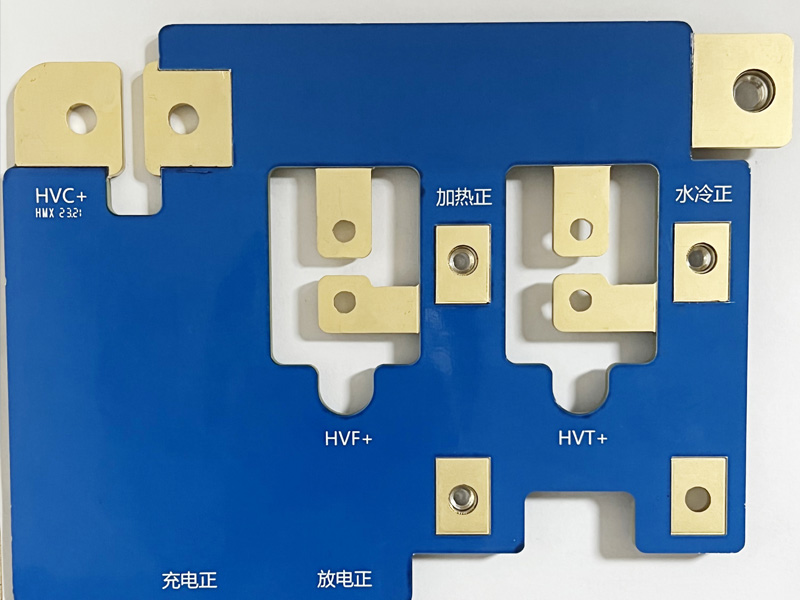
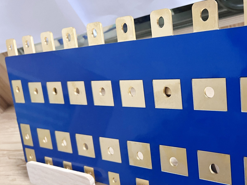
How Are Copper Busbars Integrated into PCB Designs?
In modern high-power electronics, copper busbars are no longer limited to traditional standalone metal bars. Instead, busbar PCB solutions integrate copper busbars directly into the printed circuit board. This approach provides significant advantages in terms of space efficiency, thermal management, and electrical performance.
1. Layout Design for Busbar Integration
The integration starts with careful PCB layout planning. Engineers must design the board to accommodate busbar traces that handle high currents without causing voltage drops or hotspots. Key considerations include:
Current Path Optimization: Busbar traces should follow the shortest path between power input and output points to minimize resistance.
Pad and Via Placement: Properly sized and positioned pads and vias ensure reliable soldering and mechanical stability for copper busbar PCB connections.
Segregation of High and Low Voltage Zones: Isolating high-current traces reduces the risk of interference with sensitive signals.
This design phase is critical to maximize the current carrying capacity of copper busbars while maintaining overall board reliability.
2. Copper Thickness and Material Selection
The grade of copper used in busbars and its thickness directly affect performance. Standard copper PCB layers may not suffice for high-current applications, so busbar layers often use thicker copper plating or embedded copper strips:
High-grade Copper Material: Using electrolytic tough pitch (ETP) copper or oxygen-free copper ensures low resistivity and high thermal stability.
Thickness Selection: Engineers calculate the required copper thickness based on ampacity requirements, voltage drop, and thermal limits. This ensures that the PCB copper busbar can handle the expected load without overheating.
Plating Options: Additional surface treatments such as silver-plated copper busbars or tinned copper busbars may be applied to reduce contact resistance and improve solderability.
3. Mechanical Stability and Thermal Management
Integrating copper busbars into a PCB is not only about current flow—it also involves mechanical and thermal considerations:
Structural Reinforcement: Thick busbar traces can create stress points on the PCB. Designers may use additional layers, vias, or embedded support structures to maintain mechanical integrity.
Heat Dissipation: Embedded busbars act as thermal conduits, spreading heat generated by high currents across a larger copper area. This is crucial in high-power inverters, EV battery modules, and industrial LED systems.
Flexible Busbar Layers: In some designs, flexible copper busbars or laminated copper layers are used to absorb mechanical vibration and reduce stress, improving long-term reliability.
4. Manufacturing and Integration Considerations
Implementing copper busbars in PCBs requires precise fabrication techniques:
Lamination: Multi-layer boards may have busbar layers laminated between standard signal layers.
CNC Milling or Laser Routing: Precise copper cutouts allow integration of busbar traces while avoiding short circuits or hotspots.
Quality Control: Post-fabrication testing ensures the busbar PCB meets required current ratings, thermal performance, and dimensional accuracy.
5. Applications and Performance Benefits
Integrated copper busbars enhance PCB performance in compact, high-power applications:
Electric Vehicles (EVs): Busbar PCBs efficiently distribute battery power while minimizing board space.
Industrial Inverters: High-current busbars reduce resistance and thermal stress in power conversion modules.
High-power LED Systems: Embedded busbars provide uniform current distribution, reducing voltage drops and hotspots.
Key Takeaways
Efficient Layout Design: Optimized trace paths and pad placement are critical for performance and reliability.
High-quality Copper Selection: The grade of copper used in busbars and thickness directly impacts ampacity, thermal stability, and energy efficiency.
Mechanical and Thermal Reliability: Proper reinforcement and heat management extend PCB lifespan and prevent failures.
Advanced Manufacturing: Laminated layers, precise routing, and rigorous quality control ensure safe, high-performance busbar PCB integration.
Wide Applications: EVs, industrial inverters, and high-power LEDs benefit from compact, high-efficiency busbar PCB designs.
By embedding copper busbars into PCBs, engineers achieve superior current distribution, enhanced heat dissipation, and reduced footprint, enabling modern electronics to meet ever-growing performance demands.
Why Use PCB Bus Bars?
In the past, engineers relied on widening copper traces on PCBs to handle increasing current demands. But as chips grow more powerful and compact, this traditional approach has reached its limits. Voltage drop, overheating, and wasted board space have become serious bottlenecks in modern power delivery design.
To address these challenges, PCB bus bars have emerged as an integrated solution. Acting as high-current conductors embedded directly into the PCB, bus bars provide superior conductivity, thermal performance, and mechanical strength within a compact footprint.
Core Advantages
1. Handle Extremely High Currents
Comparison: A wide copper trace might carry only tens of amps, while a PCB bus bar can handle several times—or even tens of times—more.
Reason: Much larger cross-sectional area and thickness of the bus bar.
Value: Enables designs like motor drives, power modules, and servers to handle hundreds of amps reliably.
2. Ultra-Low Impedance and Voltage Drop
Comparison: PCB copper traces have relatively higher resistance, causing voltage drops.
Reason: Bus bars use pure copper or brass with large cross-sections, ensuring very low resistance.
Value: Improves efficiency, reduces energy loss, and keeps end-voltage stable under load.
3. Superior Heat Dissipation
Comparison: Wide traces have limited heat dissipation capacity.
Reason: Bus bars act as heat sinks with high thermal mass and greater surface area.
Value: Controls hot spots, improves thermal reliability, and extends service life.
4. Saves Valuable PCB Space
Comparison: Supporting large currents with wide traces requires extensive copper layers or stacked planes.
Value: Bus bars achieve the same—or higher—current capacity in smaller areas, freeing space for more components or signal routing. This supports miniaturization and high-density layouts.
5. Mechanical Stability and Connection Reliability
Comparison: PCB pads may crack or degrade under stress from repeated connections or vibration.
Value: Bus bars provide rigid power connection points that withstand mechanical stress, ideal for battery packs, automotive systems, and heavy cabling.
6. Lower Inductance, Better Power Integrity
Comparison: Parallel traces on PCBs create higher parasitic inductance.
Value: Bus bars minimize inductance, reducing voltage spikes and noise in fast-switching power devices such as GaN or SiC semiconductors.
PCB Bus Bars vs. Traditional Methods
Think of PCB bus bars not as a universal solution, but as a strategic choice depending on your design needs:
Current above 50A? → Strongly consider bus bars.
PCB space is extremely limited? → Bus bars free up board area.
Thermal bottleneck? → Bus bars provide superior cooling.
Current below 10A and cost-sensitive? → Wide copper traces may remain more economical.
Frequent design revisions? → PCB traces are more flexible to modify than bus bar layouts.
This decision matrix helps balance performance, cost, and flexibility.
Real-World Applications
PCB bus bars shine in industries where high current, tight space, and reliability converge:
Electric Vehicles: On-board chargers, motor controllers, battery management systems.
Data Centers: Server rack power distribution, GPU cluster supplies.
Renewable Energy: Solar inverters, energy storage converters.
Consumer Electronics: High-end gaming laptops, workstation power modules.
Practical Considerations
Despite their advantages, PCB bus bars are not without trade-offs:
Cost: Extra copper material and assembly increase costs compared to traces.
Design Flexibility: Bus bar designs are less adaptable once finalized.
Assembly Complexity: May require selective soldering, press-fit, or special fixtures.
These factors should be weighed carefully during the design phase.
To conclude, as electronic systems evolve toward higher power, higher density, and higher reliability, traditional PCB traces can no longer keep up with the demands of power delivery. PCB bus bars provide a transformative solution: high current capacity, low impedance, superior cooling, space savings, and robust mechanical stability. When your project faces challenges like high current, thermal stress, or space limitations, PCB bus bars should not just be considered an alternative—but a key design option for the future.
Where to Get PCB Copper Busbar?
Finding a PCB copper busbar supplier is not as simple as comparing quotes. The wrong choice can mean delayed projects, unstable performance, or even on-site failures. To avoid costly risks, engineers must evaluate suppliers with the same rigor they apply to design decisions.
1. Technical Customization
Many suppliers sell copper busbars as generic components. But in high-power applications like EV power electronics, server racks, or industrial inverters, every design carries unique thermal, space, and vibration challenges.
At EBest Circuit (Best Technology), we treat busbars not as parts, but as engineered solutions.
Deep application knowledge: We have delivered custom Busbar PCB solutions for industries as diverse as electric vehicles, renewable energy, and data centers, where reliability under vibration and high current is non-negotiable.
Collaborative design support: Our engineers provide free DFM (Design for Manufacturability) reviews, helping optimize layouts before production begins—avoiding costly rework and shortening time-to-market.
Seamless data exchange: We support direct import of your CAD files (such as .step), ensuring precise translation of your design intent.
2. Quality Assurance
A copper busbar must not only conduct current, it must do so consistently, safely, and with long-term reliability. EBest Circuit (Best Technology)’s manufacturing backbone guarantees that consistency.
Precision fabrication: We employ high-speed CNC punching and bending, achieving dimensional tolerances within ±0.05mm for flawless assembly.
Flexible surface treatments: Options such as tin, silver, or nickel plating improve conductivity, corrosion resistance, or solderability, chosen based on your application’s requirements.
Certified quality systems: With IATF16949, ISO9001, ISO13485, and AS9100D certifications, combined with 100% continuity testing, every product leaves our line backed by documented reliability.
3. End-to-End Service and Support
Ordering a custom PCB busbar is more than just a purchase—it’s a project. EBest Circuit (Best Technology) supports you through every stage:
Rapid prototyping: Prototypes delivered in as little as 3–5 days, enabling fast design iterations.
Scalable production: Whether you need small pilot runs or high-volume manufacturing, we adapt to your product lifecycle.
Transparent project management: Each project is assigned a dedicated manager, keeping you informed with real-time production updates.
Fundamentally, choosing a PCB copper busbar supplier is not about the lowest quote. It is about finding a partner who understands your application, delivers uncompromising quality, supports you through the process, and offers real long-term value. EBest Circuit (Best Technology) is more than a manufacturer—we are a strategic partner who combines engineering expertise, proven quality, and reliable service to help you achieve safe, efficient, and future-ready power solutions.
In essence, understanding copper busbar fabrication and its integration into PCB (Printed Circuit Board) solutions is crucial for modern high-power electronics. Partnering with EBest Circuit (Best Technology) resolves common challenges in your Busbar PCB projects, such as voltage drop, space constraints, and thermal management. Pls send your design sketch or requirements to sales@bestpcbs.com for a quick, free review and quote. Our certified processes, customization options, and engineering expertise deliver reliable busbar PCB solutions that boost performance, helping you achieve superior results in demanding electrical applications.