

How to design a castellated PCB? This blog is mainly about design guideline and considerations, production process for castellated PCB.
Are you troubled these issues with castellated PCB?
- Is board space extremely limited while traditional connections occupy too much area and fail reliability?
- When welding modules to mainboards, is alignment often imprecise, causing high yield fluctuations and production costs?
- Want compact board-to-board assembly but face complex processes, long cycles, and struggle to match product iteration speeds?
As a castellated PCB manufacturer, EBest Circuit (Best Technology) can provide you service and solutions:
- Process Guarantee: Specializing in castellated PCB precision machining, we use unique processes and full-cycle quality control to ensure full copper plating, smooth hole walls, and stable “golden fingers” for reliable board connections.
- Design Collaboration Optimization: Professional front-end DFM analysis services identify design-phase risks early, optimizing module layouts and castellated structures for precise alignment and efficient assembly.
- Efficient Flexible Production: Rapid-response production lines for small/medium batches reduce lead times, flexibly align with R&D rhythms and market demands, and accelerate market entry.
Feel free to contact us if you have inquiry for castellated PCB: sales@bestpcbs.com.
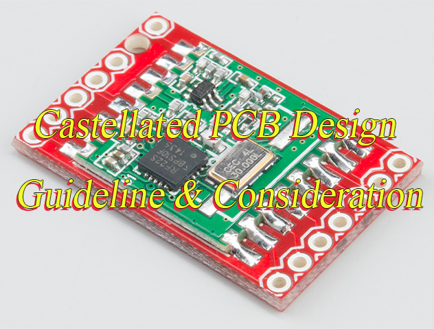
What Is a Castellated Hole PCB?
A Castellan Hole PCB is a type of printed circuit board with specially designed semi-circular gold-plated holes (resembling castle crenellations) machined along its edges. Its core feature is that these holes are precisely cut into half-holes along the board edge, and the hole walls are metallized, exposing the internal conductor layers. This design allows the PCB to be soldered directly to the pads of another PCB through the metallized layer on the half-hole, just like surface mount technology (SMT) components, achieving a reliable vertical interconnection between boards.
Why Use Castellated Holes in PCB?
- Achieving Vertical Board-to-Board Interconnection: Core Advantages. Allows one PCB to be directly and vertically soldered to the pads of another PCB via a metallized layer on a half-hole, just like a surface mount device (SMT) component, creating a compact 3D structure.
- Significant Space Savings: Vertical stacking greatly optimizes the utilization of internal space, especially suitable for space-constrained miniaturized and portable electronic products.
- Simplified Assembly Process: Eliminates the need for additional connectors such as sockets, pin headers, cables, or flexible printed circuit boards (FPCs) required for traditional board-to-board connections, reducing material costs and assembly steps.
- Improved Connection Reliability: Direct SMT solder joints are formed between the metallized half-holes and the pads, providing stronger mechanical strength and electrical contact reliability than plug-in connectors, and offering better vibration resistance.
- Reduced Overall Cost: By eliminating external connectors and their assembly costs, and simplifying the production process (compatible with standard SMT processes), the bill of materials (BOM) and manufacturing costs of the product can be effectively reduced.
- Enhanced Design Flexibility: Facilitates modular design. Functional modules (such as Wi-Fi/BT modules and power modules) can be prefabricated as independent daughterboards with castle holes, simplifying the main system design and facilitating replacement and upgrades.
How To Design A Castellated PCB?
1. Define Design Goals and Constraints
- Functional Requirement Definition: Engage in in-depth communication with clients to clarify electrical performance (e.g., signal speed, impedance requirements), mechanical dimension constraints (e.g., castellation pitch, height), thermal management needs (e.g., heat dissipation path, power dissipation), and environmental adaptability (e.g., temperature range, vibration resistance).
- Standards and Specification Compliance: Adhere to international standards (e.g., IPC-2221A, IPC-4761) and client-specific specifications, including EU RoHS/REACH environmental requirements and UL safety certifications.
- Castellation Feature Design: Determine geometric parameters for sawtooth edges (e.g., tooth width, pitch, height). Typically, tooth width ≥1.5mm ensures mechanical strength, pitch matches assembly tolerances (e.g., ±0.1mm), and height integrates thermal requirements (e.g., 30% surface area increase).
2. Stack-Up Structure and Material Selection
- Layer Stack Planning: Design stack-up based on signal integrity needs. For high-speed digital circuits, use 6-layer structures (signal-ground-power-signal-ground-signal) to ensure impedance continuity (e.g., 50Ω single-ended, 100Ω differential).
- Material Selection: Choose high-frequency/high-speed substrates (e.g., Rogers 4350B, Isola I-Tera MT40) to reduce dielectric loss, or high-Tg materials (Tg ≥170°C) for thermal stress resistance. Copper thickness matches current capacity (e.g., 1oz for signal layers, 2oz for power layers).
- Ground Plane Design: Implement continuous ground planes covering critical signal areas to minimize signal return paths. Use thin dielectrics (e.g., 50μm) between power and ground planes to reduce PDN impedance.
3. Layout and Routing Strategies
- Layout Principles: Partition functional modules (digital, analog, power zones). Place sensitive components (e.g., crystal oscillators) away from heat sources and noise sources. Avoid precision components near castellation edges to prevent mechanical stress damage.
- Routing Rules: Route high-speed signals as differential pairs (length matching ±5mil, spacing ≥3× line width). Avoid 90° turns (use 45° or curved paths). Calculate power trace width for current capacity (e.g., 10mil width for 1A current) and use multiple vias for parallel resistance reduction.
- Castellation Edge Handling: Add non-functional pads (e.g., 1mm×1mm) at sawtooth edges for mechanical reinforcement. Chamfer edges (e.g., R0.5mm) to reduce stress concentration.
4. Thermal Design and Heat Management
- Heat Dissipation Path Planning: Place high-power devices (e.g., power MOSFETs) over thick copper pours (≥2oz) and connect to ground planes via thermal vias filled with solder paste. Design castellation edges as heat sinks to increase air contact area.
- Thermal Via Design: Deploy dense thermal vias (e.g., 0.3mm diameter, 1mm spacing) under heat sources to form thermal channels. Fill vias with conductive materials (e.g., copper paste) to enhance thermal conductivity.
- Simulation Validation: Use thermal simulation tools (e.g., ANSYS Icepak) to verify temperature distribution, ensuring peak temperatures stay below component limits (e.g., junction temperature ≤125°C).
5. Signal Integrity and EMC
- Impedance Control: Calculate stack-up parameters to ensure critical signal line impedance matching (e.g., using Polar SI9000). Apply back-drilling to minimize stub effects.
- Crosstalk Mitigation: Increase shielding for sensitive signals (e.g., 3W rule) or use ground shielding. Maintain sufficient spacing between high-speed differential pairs (≥3× line width).
- EMC Design: Add π-type filters (inductor + capacitor) at power entry points. Place decoupling capacitors (e.g., 0.1μF + 10μF) near critical ICs. Avoid antenna effects at castellation edges (e.g., long traces).
6. Testability and Reliability
- Test Point Design: Place test pads (≥1mm diameter) at critical nodes (power, signal I/O) with labeled identifiers. Boundary scan (JTAG) interfaces must comply with IEEE 1149.1.
- Mechanical Reliability: Validate vibration resistance via stress analysis (e.g., ANSYS Mechanical). Reinforce critical connector areas with stiffeners (e.g., L-shaped copper traces).
- DFM Checks: Perform DRC/ERC checks using EDA tools (e.g., Altium Designer, Cadence Allegro) to ensure compliance with manufacturing tolerances (e.g., minimum trace/spacing ≥4mil). Generate Gerber files and drilling data.
7. Testability and Reliability
- Design Documentation: Compile detailed specifications (BOM, stack-up, routing rules), assembly drawings, and test procedures. Provide 3D models (e.g., STEP format) for mechanical fit evaluation.
- Version Control: Track design changes using version control systems (e.g., Git) for traceability. Final deliverables include Gerber files, BOM, coordinate files, and process notes.
Castellation PCB Design Technical Parameter
| Parameter Name | Recommended Value/Range |
| Drill Diameter | 0.4 mm – 1.0 mm |
| Pad Diameter | Drill Diameter + 0.2 mm |
| Depth | Board Thickness |
| Pitch | ≥ 0.5 mm (High-density designs may reduce to 0.4 mm with DFM evaluation) |
| Edge Clearance | ≥ 0.3 mm |
| Cu Plating Thickness | Minimum 20 μm (0.8 mil) |
| Surface Finish | ENIG / HASL / Immersion Tin |
| Hole Wall Roughness | ≤ 35 μm |
| Burr Control | No visible burrs |
| Solder Mask Opening | Single-side expansion 0.05-0.1 mm |
| Thermal Shock Test | -40°C to +125°C |
| Solderability | Wetting area ≥95% |
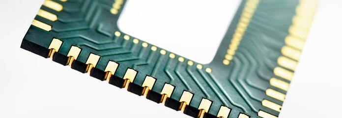
PCB Castellated Edges Design Consideration
Mechanical Strength and Dimensional Design
- Minimum Hole Diameter Requirements: PCB half-hole diameter must be determined based on board thickness. For boards under 1.0mm thick, a minimum half-hole diameter of 0.6mm is recommended; for boards over 1.6mm thick, a minimum half-hole diameter of 1.0mm is advised.
- Edge Spacing: Maintain a minimum distance of 10–15% of board thickness between half-hole edges and outer copper foil edges to minimize stress concentration and ensure soldering quality.
- Pattern Consistency and Alignment: Precise alignment between pads and drilled holes is critical. Include adequate fiducial marks to reduce component misalignment risks.
Electrical Signal Integrity
- Reference Layer Management: Avoid cutting through power and ground planes near half-holes. Implement reference layer bridging (keep-out area bridge design) to mitigate impedance mismatches.
- Shielding Design: For RF/high-frequency applications, incorporate metallized shielding edges and alternating pad layouts to reduce EMI.
- Coaxial Signal Path Recommendations: When routing high-speed differential lines, maintain consistent spacing along pads. For high-density communication modules, perform impedance simulation to validate design parameters.
Process Standardization
- Pad Geometry Design: Half-hole pads should be oval-shaped or extended to the edge to ensure adequate plating coverage (≥65% metal retention post-drilling).
- Pre-Soldering Preparation: Apply epoxy hole fill or solder mask control in half-hole soldering zones to enhance SMT reliability.
- Plating and Surface Coating: Use ENIG (Electroless Nickel Immersion Gold) or immersion tin for full-board plating. Employ step plating to ensure uniform metallization in half-hole walls.
Manufacturing Compatibility
- Process Time and Cost: Many international PCB fabricators require high-precision milling tools for panelized half-hole cutting. Confirm equipment capabilities support continuous half-hole slot cutting dimensions.
- Thermal Stress Optimization: Integrate thermal relief designs aligned with end-device thermal cycling profiles to prevent soldering failures from thermal cycling.
Testing and After-Sales Support
- ICT Interface Design: Include test points in the layout to accommodate FCT (Functional Circuit Test) tooling customization.
- Documentation Clarity: Clearly annotate half-hole positions in assembly diagrams to prevent reflow misalignment.
- Failure Diagnostics Support: Document common failure modes (e.g., insufficient solder, terminal lifting) with inspection guidelines and troubleshooting steps.
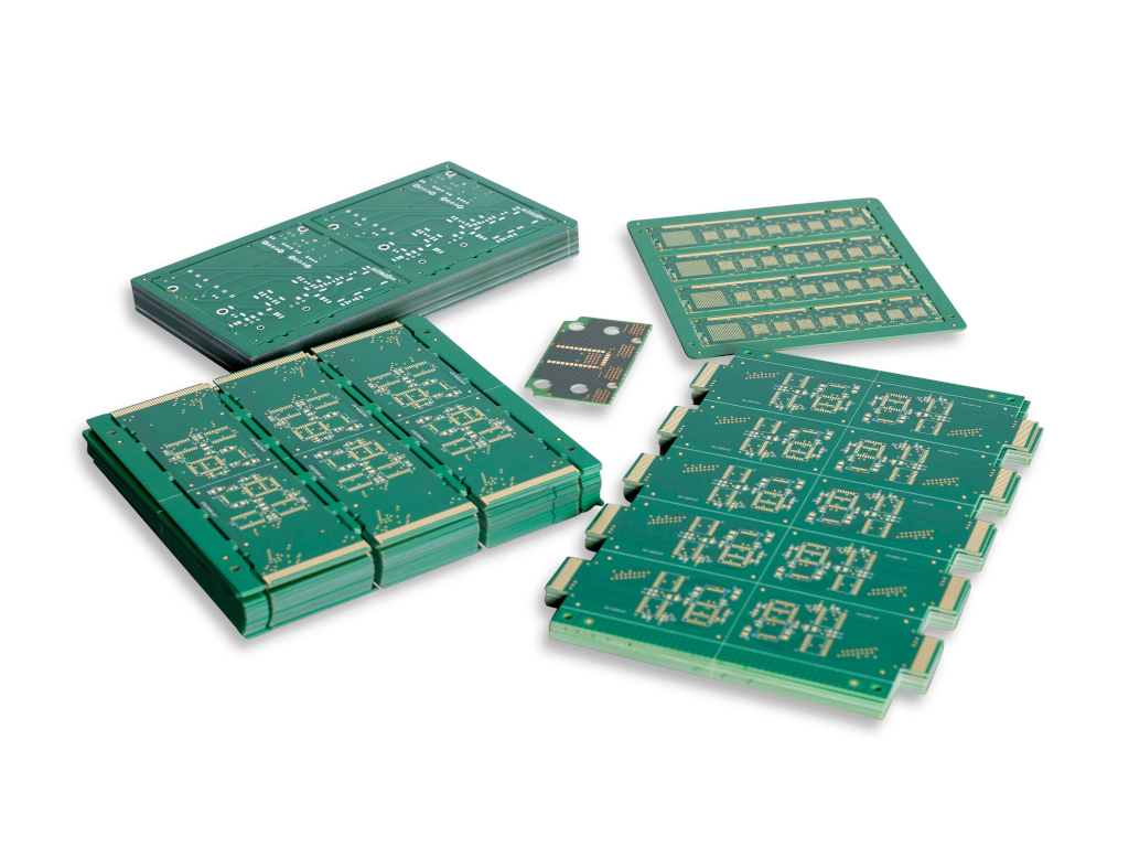
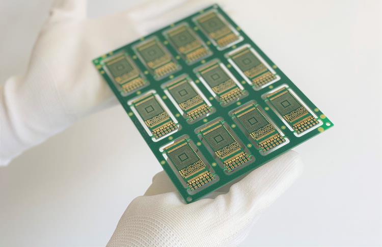
How to Make A Castellated PCB?
1. Substrate Preparation and Lamination
- Material Selection: Choose FR-4, high-frequency materials, or flexible substrates, coated with electrolytic copper foil (thickness ≥35μm) to ensure conductivity and mechanical strength.
- Lamination Process: Bond inner core boards, prepregs (PP), and outer copper foils through high temperature and pressure to form a multi-layer structure, controlling interlayer alignment accuracy to ±0.05mm.
2. Drilling and Plating
- Full Hole Drilling: Drill complete through-holes (diameter 0.6-1.2mm) at the board edge using tungsten carbide drills or laser drilling (for HDI boards with hole diameters ≤0.1mm).
- Hole Metallization: Apply chemical copper deposition (0.3-1μm) to cover the hole walls, followed by electroplating to thicken the copper layer to 25-30μm, ensuring electrical connectivity. Use pulse plating or electroless copper plating to avoid copper layer tearing.
3. Outer Layer Circuit Formation
- Photolithography and Etching: Apply film, exposure, and development to form etch-resistant patterns, then etch away unprotected copper to retain circuits and copper in the half-hole area. After stripping the film, perform secondary copper/tin plating for protection.
- Solder Mask and Silkscreen: Spray liquid photoimageable solder mask, UV cure to form the solder mask layer (with precise openings), and silkscreen identification information to prevent solder bridging.
4. Half-Hole Shaping
- Cutting Process: Use precision milling cutters (double-V shaped tool path) or laser cutting along the hole center to retain the half-hole structure. Optimize spindle speed and feed rate with slot cutters to reduce burrs and copper lifting.
- Deburring: After cutting, use alkaline etching or red tape to bond unit boards and remove residual copper filaments, ensuring smooth, defect-free half-hole edges.
5. Surface Finish
- Enhanced Solderability: Apply ENIG, OSP, or immersion tin to improve pad solderability and oxidation resistance. For high-frequency applications, use immersion silver or gold plating.
- Solder Mask Bridge Design: Set a solder mask bridge of ≥0.1mm between half-holes to prevent solder short circuits. Use NSMD design in non-solder mask areas to enhance solder joint reliability.
6. Profiling and Testing
- Outline Cutting: Use CNC milling or V-cut to cut the final outline, ensuring dimensional accuracy.
- Electrical Testing: Perform flying probe or ICT testing for continuity and insulation resistance. Use AOI/AXI to inspect pad alignment and inner layer defects.
- Reliability Verification: Conduct high-temperature aging, thermal shock, and vibration tests to verify mechanical strength and electrical performance (e.g., IPC Class 3 standards).
7. Quality Control and DFM Optimization
- Precision Control: Monitor dimensional deviations in drilling, lamination, and cutting to avoid inconsistent half-hole sizes due to swelling or shrinkage.
- DFM Guidelines: Follow manufacturer guidelines (e.g., minimum hole diameter 0.5mm, edge gap 0.5mm) and optimize designs to reduce manufacturing difficulty and costs.
Why Choose EBest Circuit (Best Technology) as Castellated PCB Manufacturer?
Reasons why choose us as castellated PCB manufacturer:
- Free DFM Analysis: Professional team provides free Design for Manufacturability (DFM) analysis to identify potential manufacturing defects at the design stage, reducing trial production costs and time by over 30% for a one-time successful design.
- End-to-End One-Stop Service: Comprehensive services from design optimization and rapid prototyping to mass production delivery. Single point of contact handles all processes, boosting efficiency by 40% and ensuring smooth project progression.
- 1 Piece MOQ: Supports small-batch and single-piece orders to meet prototype validation and small-scale trial production needs, lowering initial investment risks and enabling rapid design iteration to capture market opportunities.
- 19 Years of Technical Expertise: Deep experience in PCB manufacturing with over 5,000 complex projects completed. Specializes in high-density interconnect (HDI) and miniaturized designs to ensure flawless execution of innovative concepts.
- Globally Recognized Quality Certifications: Holds ISO 13485 (medical), AS9100D (aerospace), and IATF 16949 (automotive) certifications, meeting stringent requirements for high-reliability applications in medical, aerospace, and automotive sectors.
- Custom Material Solutions: Offers tailored material options including ultra-thin substrates, high-frequency high-speed materials, and high-temperature specialty materials to match diverse application scenarios from consumer electronics to industrial controls.
- Engineer-Centric Support: Bilingual technical team provides 24/7 support, covering design specification interpretation and production issue diagnosis to reduce communication costs and ensure project success.
- Eco-Friendly Manufacturing Commitment: Utilizes lead-free processes and wastewater recycling systems compliant with RoHS/REACH standards, facilitating seamless international environmental certification and enhancing global market access.
Welcome to contact us if you have any request for castellated PCB: sales@bestpcbs.com.