

Burn-in test plays a critical role in electronics manufacturing where long-term reliability matters as much as performance. Engineers often rely on burn-in procedures to expose early-life failures before products reach the field. Whether used for high-reliability PCBA, industrial controllers, or medical electronics, this method helps stabilize product quality while reducing unexpected returns.
Below is a practical, engineering-focused guide explaining how burn-in testing works, why it matters, and how it applies specifically to PCB assemblies.
What Is a Burn-In Test in Electronics?
A burn-in test is a reliability testing process used in electronics manufacturing to identify early-life failures in electronic components, PCBs, and assembled electronic products.
During a burn-in test, electronic devices are operated under elevated stress conditions—such as higher temperature, voltage, or load—over a defined period of time. Components that are defective or marginal are more likely to fail during this phase rather than later in real-world use.
In simple terms:
Burn-in testing accelerates failure so weak components fail early—before products reach customers.
Burn-in tests are widely used in:
- PCB manufacturing and PCB assembly (PCBA)
- Power electronics
- Automotive electronics
- Aerospace and defense systems
- Medical devices
- Industrial control equipment
- Telecommunications hardware
Burn-in Testing
What Is the Purpose of a Burn-In Test?
The primary purpose of a burn-in test is to improve product reliability and reduce field failures.
More specifically, burn-in testing is designed to:
- Detect early-life failures (infant mortality)
- Screen out defective components
- Verify design robustness
- Stabilize electrical performance
- Reduce warranty returns and RMA costs
Electronics failures often follow the bathtub curve, where failure rates are high at the beginning, low during normal life, and rise again at end-of-life. Burn-in testing targets the first phase of this curve.
Why Is a Burn-In Test Important?
Burn-in testing plays a critical role in quality assurance (QA) and reliability engineering.
Key Benefits of Burn-In Testing
1. Reduces Early Field Failures
Burn-in tests catch problems such as:
- Poor solder joints
- Marginal ICs
- Weak capacitors
- Manufacturing defects
- Thermal design issues
2. Improves Brand Reputation
Products that fail shortly after installation damage customer trust. Burn-in testing helps ensure only stable and reliable products ship.
3. Saves Cost in the Long Term
While burn-in testing adds upfront cost, it significantly reduces:
- Warranty claims
- Product recalls
- Field repair costs
- Customer downtime
4. Required by High-Reliability Industries
Industries such as medical, aerospace, automotive, and military electronics often require burn-in testing as part of regulatory or contractual standards.
How to Do a Burn-In Test?
A burn-in test procedure varies depending on the product, industry, and reliability requirements, but the core steps are similar. Typical burn-in test procedure including:
Step 1: Visual & Electrical Pre-Inspection
Before burn-in:
- Visual inspection (AOI or manual)
- Basic electrical tests (continuity, shorts, power-on test)
- Ensure boards are safe to energize
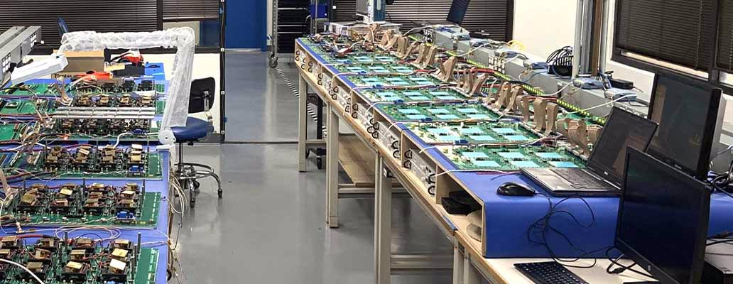
Step 2: Load the PCB or Device into Burn-In Fixtures
PCBs or assemblies are mounted in:
- Burn-in racks
- Test sockets
- Custom fixtures
- Edge connectors or cable harnesses
Fixtures allow:
- Power supply access
- Signal monitoring
- Temperature exposure
Step 3: Apply Electrical Stress
The device is powered on continuously or in cycles using:
- Rated voltage or slightly elevated voltage
- Simulated operating loads
- Functional test patterns
Step 4: Apply Thermal Stress
Temperature is raised using:
- Burn-in ovens
- Environmental chambers
- Heated racks
Typical burn-in temperatures:
- 55°C to 85°C for commercial electronics
- 85°C to 125°C for industrial or automotive electronics
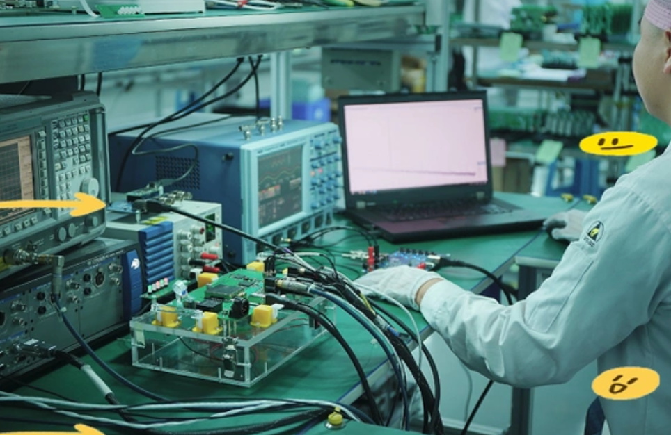
Step 5: Continuous Monitoring
During the test:
- Voltage and current are monitored
- Functional signals are checked
- Failures are logged automatically or manually
Step 6: Post Burn-In Inspection
After burn-in:
- Functional testing
- Electrical performance verification
- Visual inspection for thermal damage
- Failed units are analyzed and scrapped or repaired
What Equipment Is Needed for Burn-In Testing?
Burn-in testing requires specialized equipment to safely operate electronics under stress for long periods.
Common Burn-In Test Equipment
1. Burn-In Chambers / Ovens
- Temperature-controlled environments
- Uniform heat distribution
- Safety protection and airflow control
2. Burn-In Racks & Fixtures
- Hold PCBs or assemblies vertically or horizontally
- Provide power and signal connections
- Custom-designed for product type
3. Power Supplies
- Stable, programmable DC power supplies
- Over-current and over-voltage protection
4. Data Acquisition & Monitoring Systems
- Voltage/current monitoring
- Temperature sensors
- Failure logging software
5. Functional Test Systems
- Automated test equipment (ATE)
- Simulated loads
- Communication interfaces (RS485, CAN, Ethernet, etc.)
How Long Is a Burn-In Test?
The duration of a burn-in test depends on:
- Product complexity
- Reliability requirements
- Industry standards
- Cost considerations
Typical Burn-In Test Duration
| Application | Burn-In Time |
| Consumer electronics | 8–24 hours |
| Industrial electronics | 24–72 hours |
| Automotive electronics | 72–168 hours |
| Aerospace / military | 168–500+ hours |
Shorter burn-in tests are often used for screening, while longer tests are used for qualification and validation.
Burn-In Test for PCB and PCBA
A burn in test for PCB or PCBA focuses on identifying assembly-related and component-level issues.
What Burn-In Testing Detects in PCBs
- Cold solder joints
- Micro-cracks in solder
- Poor component placement
- Thermal expansion issues
- Marginal ICs
- Power instability
PCB Burn-In vs Functional Testing
| Test Type | Purpose |
| Functional Test | Verifies correct operation |
| Burn-In Test | Screens early failures |
| Thermal Cycling | Tests expansion/contraction |
| HALT/HASS | Stress limit testing |
Burn-in testing is not a replacement for functional testing—it is a complementary reliability process.
How to Tell If a Circuit Board Is Burnt?
A burnt PCB usually shows visible, electrical, or functional symptoms.
Visual Signs of a Burnt PCB
- Discoloration (brown or black areas)
- Burn marks or charring
- Melted solder or components
- Cracked IC packages
- Delaminated PCB layers
Electrical Symptoms
- Short circuits
- Abnormal current draw
- Voltage drops
- Failure to power on
Functional Symptoms
- Intermittent operation
- Random resets
- Overheating
- Communication errors
Burn-in testing often reveals latent damage that may not be obvious in quick functional tests.
Can a Burnt PCB Be Repaired?
Whether a burnt PCB can be repaired depends on damage severity.
Repairable Cases
- Burnt passive components (resistors, capacitors)
- Minor trace damage
- Isolated solder joint failures
Non-Repairable Cases
- Carbonized PCB substrate
- Internal layer damage (multilayer PCB)
- Widespread delamination
- Repeated thermal failure
In high-reliability industries, burnt PCBs are usually scrapped, not repaired, due to long-term reliability risks.
Burn-In Test vs Other Reliability Tests
| Test Method | Main Purpose |
| Burn-In Test | Early failure screening |
| Thermal Cycling | Mechanical stress testing |
| HALT | Find design limits |
| HASS | Production screening |
| Aging Test | Long-term performance |
Burn-in testing remains one of the most cost-effective reliability screening methods in electronics manufacturing.
FAQs
1. Is burn-in testing mandatory?
No, but it is highly recommended for high-reliability or mission-critical electronics.
2. Does burn-in testing damage electronics?
When properly controlled, burn-in testing does not damage good products—it only accelerates failure in weak units.
3. What temperature is used in burn-in testing?
Typically 55°C to 125°C, depending on component ratings and standards.
4. Is burn-in testing expensive?
It adds cost, but often reduces total lifecycle cost by preventing failures in the field.
5. Can burn-in testing replace functional testing?
No. Burn-in testing supplements functional and electrical testing.
6. What standards reference burn-in testing?
Common references include:
- MIL-STD-883
- JEDEC standards
- IPC reliability guidelines