

Among the most widely used test solutions in PCB and PCBAs are bed of nails test (fixture-based in-circuit testing) and flying probe testing. Although both serve the same core purpose—validating electrical integrity—their cost models, speed, scalability, and production suitability differ significantly. Tolday, we will introduce the main differences between them, their cost and functions.
What Is Bed of Nails Testing?
A bed of nails test is a traditional yet highly effective in-circuit testing (ICT) method used in PCB and PCBA manufacturing. It employs a dedicated mechanical fixture populated with hundreds or even thousands of spring-loaded contact probes—commonly called pogo pins—that simultaneously touch predefined test pads on a circuit board.
The objective is straightforward: validate electrical integrity at the component level. This includes verifying:
- Open and short circuits
- Component presence and polarity
- Resistance, capacitance, and diode values
- Basic functional parameters
Unlike functional testing, which evaluates system behavior, a bed of nails pcb test fixture focuses on granular electrical correctness. It is widely adopted in high-volume production where repeatability, speed, and per-unit cost efficiency are critical.

What Is the Nail Bed Test a Way of Checking For?
A nail bed test primarily checks manufacturing defects introduced during PCB fabrication or SMT assembly. It is not meant to validate firmware or full system functionality. Instead, it answers one practical question:
“Is the board electrically assembled exactly as designed?”
Typical defect categories detected by a bed of nails test include:
| Defect Type | Example | Detection Capability |
| Open circuits | Broken trace, unsoldered lead | Excellent |
| Shorts | Solder bridge between pads | Excellent |
| Wrong component value | 10kΩ installed instead of 1kΩ | Excellent |
| Missing component | Unplaced resistor/capacitor | Excellent |
| Reversed polarity | Electrolytic capacitor, diode | Excellent |
| Functional logic errors | MCU firmware bug | Not covered |
In high-reliability sectors—industrial control, automotive electronics, medical equipment—ICT remains a cornerstone quality gate before burn-in or functional testing.
How Does a Bed of Nails Tester Work?
The operating principle is mechanical precision combined with electrical measurement.
1. Fixture Alignment
The PCB is positioned onto a custom-machined fixture base.
2. Compression Contact
A pneumatic or mechanical press lowers the PCB onto an array of spring-loaded probes.
3. Electrical Interface
Each probe makes contact with a designated test pad, creating a temporary conductive path.
4. Measurement Execution
The ICT system injects small currents or voltages and measures electrical responses.
5. Data Evaluation
The system compares readings against tolerance windows defined by test programming.
Because all nodes are accessed simultaneously, test time is extremely short—often under 30 seconds for complex boards. This speed makes the bed of nails test fixture ideal for medium-to-high volume manufacturing where throughput matters.
Bed of Nails Test Pins Overview
The reliability of a bed of nails test heavily depends on the quality of its test probes. Core Characteristics of Bed of Nails Test Pins:
- Spring-loaded mechanism for consistent pressure
- Gold-plated tips for low contact resistance
- Various tip geometries: crown, spear, flat, concave
- Rated lifecycle: typically 100,000–1,000,000 cycles
Pin selection depends on:
- Pad surface finish (ENIG, HASL, OSP)
- Test pad diameter
- Required current rating
- Board thickness and rigidity
Proper probe force calibration is essential. Excessive pressure risks pad damage; insufficient pressure leads to unstable readings.
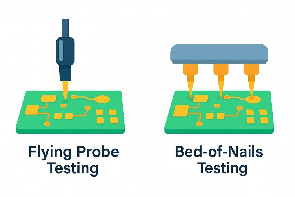
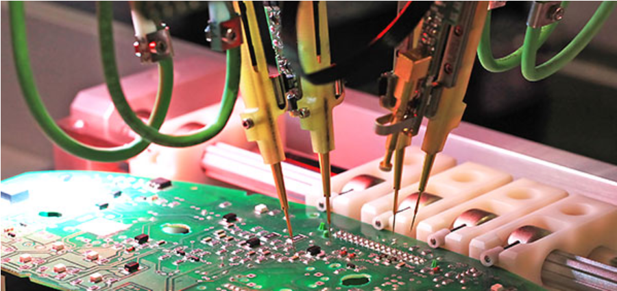
What Is the Difference Between Flying Probe and Bed of Nails?
In PCB testing, fixture testing (commonly referring to bed of nails testing or dedicated ICT fixtures) and flying probe testing are two mainstream electrical inspection methods. They differ significantly in working principle, cost structure, efficiency, flexibility, and suitable production scenarios.
Below is the translated comparison based directly on the existing table structure:
| Feature | Bed of Nails Testing (Fixture Testing) | Flying Probe Testing |
| Working Principle | Uses a custom dedicated fixture populated with spring-loaded probes (pogo pins). The PCB is pressed down once to contact all test points simultaneously for parallel testing. | Uses 4–8 movable precision probes that contact PCB test points sequentially according to programmed paths. No dedicated fixture is required. |
| Testing Speed | Extremely fast, suitable for mass production. A single test cycle typically takes only a few seconds. | Slower, because probes must move point-by-point. Test time increases significantly as the number of test points grows. |
| Initial Cost | High. Each PCB design requires a dedicated fixture. Typical fixture cost ranges from $5,000 to $20,000 or more. Development cycle is longer. | Low. No custom fixture is required. Equipment programming is flexible. Ideal for new product development and small-batch trial production. |
| Per-Unit Testing Cost | Very low in mass production. Per-board test cost can drop to around $0.1 when volumes are high. | Relatively higher. Typical per-board cost ranges from $2 to $5. Cost advantage is mainly reflected in small-batch production. |
| Application Scenario | Large-scale production (monthly volume >500 units), fixed test points, stable PCB design. | Small-batch production, sample validation, R&D stage, frequent model changes, or high-density PCBs (e.g., 0.05 mm pitch) with limited test access. |
| Flexibility | Low. One fixture is dedicated to one PCB design. A new fixture must be built for each revision. | High. The same equipment can quickly adapt to different PCB models and sizes through software reprogramming. |
| Testing Capability | Supports in-circuit testing (ICT) and functional testing (FCT). Capable of component measurement, insulation resistance testing, and impedance testing. | Primarily used for open/short detection and basic component measurement. Some high-end systems support high-voltage testing, but complex functional coverage may be limited. |
| Maintenance & Durability | Test probes (pogo pins) have long lifespans (hundreds of thousands of cycles), but fixture mechanical structure is complex and maintenance cost is higher. | Probes are consumable parts and require frequent replacement, but overall machine structure is relatively simpler. |
For 10,000+ unit production runs, bed of nails test becomes cost-effective. For prototypes or high-mix low-volume, flying probe offers flexibility.
Many factories use both methods depending on product lifecycle stage.
How Accurate Is a Nail Bed Test for PCBs?
Accuracy in a bed of nails test environment is typically very high for electrical continuity and component validation.
Key factors influencing accuracy:
- Probe contact resistance stability
- Fixture mechanical alignment tolerance
- Test programming margin calibration
- Environmental factors (humidity, contamination)
Modern ICT systems achieve measurement precision in the milliohm and picofarad range.
However, limitations exist:
- Cannot detect intermittent faults caused by mechanical stress
- Limited functional verification capability
- Complex BGA nodes may require boundary scan integration
Therefore, bed of nails testing is often combined with:
- AOI
- X-ray inspection
- Functional test (FCT)
- Burn-in test
How to Design Bed of Nails Test Fixture?
Fixture design directly impacts coverage, durability, and long-term ROI.
1. DFT (Design for Testability)
Before fixture development, PCB layout must incorporate:
- Dedicated test pads (≥0.8mm preferred)
- Adequate pad spacing
- Clear probe access areas
- Ground reference points
Early DFT collaboration reduces fixture complexity.
2. Mechanical Structure
Typical fixture components:
- FR-4 or aluminum base plate
- Probe plate
- Guide pins
- Top pressure plate
- Vacuum or pneumatic press mechanism
For multilayer or flex boards, support tooling is necessary to prevent warpage.
3. Electrical Interface
Fixture wiring routes each probe to:
- ICT system connector
- Switching matrix
- Signal conditioning modules
High-density boards may require double-sided probing.
4. Maintenance Planning
Good fixture design considers:
- Replaceable probe modules
- Easy cleaning access
- Wear part lifecycle tracking
A well-designed bed of nails pcb test fixture can support years of high-volume production.
How Much Does a PCB Bed of Nails Test Fixture Cost?
Cost varies significantly depending on complexity.
Typical Cost Range:
| Board Complexity | Estimated Fixture Cost |
| Simple 2-layer board | $150 – $500 |
| Mid-complexity SMT board | $500 – $1000 |
| High-density multilayer | $2000 – $4000+ |
Cost factors include:
- Probe count (each probe adds cost)
- Double-sided access
- Precision machining requirements
- Interface adapter type
- Programming and validation effort
Although initial cost appears high, amortization over large production volumes significantly reduces per-unit test expense.
Bed of Nails Testing – Frequently Asked Questions
1. Is bed of nails test suitable for prototype boards?
Generally not economical unless volumes exceed several thousand units. Flying probe testing is more practical for early design validation.
2. Can bed of nails test access BGA signals?
Only if dedicated test vias or pads are designed. Otherwise, boundary scan (JTAG) integration is required.
3. How long does fixture development take?
Typically 2–4 weeks depending on board complexity and DFT readiness.
4. How many test points are needed?
It depends on required coverage. High-reliability industries often aim for >85% electrical coverage.
5. Do test probes damage PCB pads?
When correctly specified and calibrated, probe contact is non-destructive. Excessive pressure or poor maintenance can cause pad wear.
6. What is the lifecycle of a bed of nails fixture?
With maintenance, fixtures commonly exceed 100,000+ test cycles.