pcb
Home > Blog

Posts Tagged ‘annular ring pcb’

Annular Ring PCB, Annular Ring in PCB Design & Manufacturer
Monday, May 26th, 2025

Looking for annular ring PCB solutions? Let’s dive into its benefits, application, design tips, and why choose Best Technology as an annular ring PCB partner.

What Is Annular Ring In PCB?

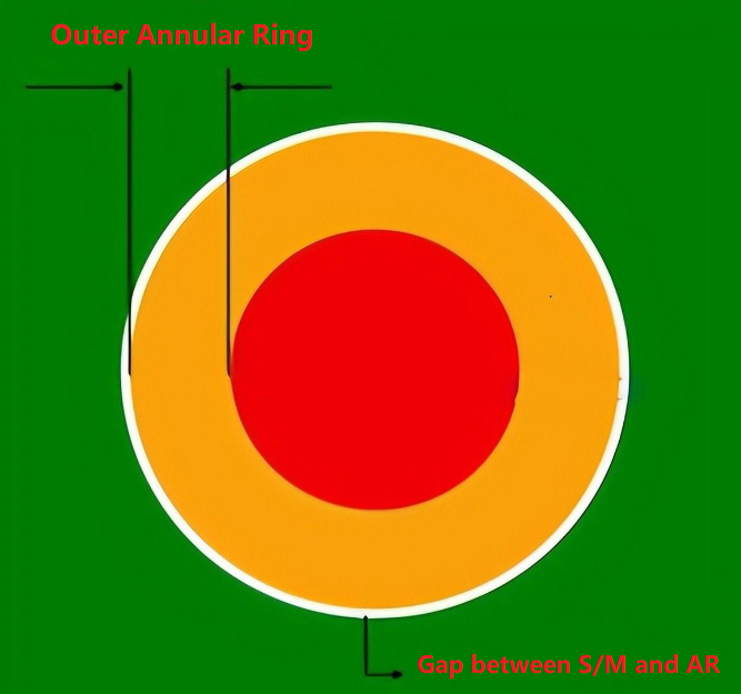
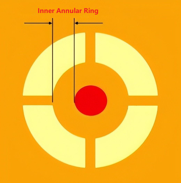
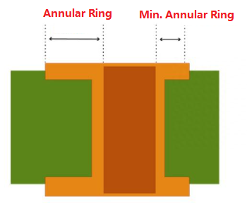
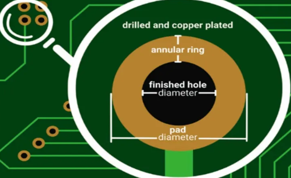
Annular ring in PCB refers to the copper pad area that surrounds a drilled hole, typically used for vias or component mounting. It is the conductive material that connects the hole to the surrounding traces or planes. The annular ring is a critical aspect of PCB design, as it ensures proper electrical connectivity and mechanical stability for components and vias.

Annular ring in PCB

Why Is the Annular Ring PCB Important?

The annular ring plays a vital role in PCB functionality and reliability. Here’s why it matters:

  • Electrical Connectivity: Ensures reliable connections between holes (e.g., via, component pins) and surrounding circuitry by maintaining sufficient copper contact around drilled holes.
  • Mechanical Stability: Reinforces the structural integrity of holes, reducing risks of pad lift-off or breakage during assembly, thermal cycling, or mechanical stress.
  • Manufacturing Tolerance Compensation: Acts as a buffer for drilling misalignment, ensuring the hole remains within the conductive pad area even with slight positional deviations.
  • Signal Integrity: Minimizes impedance discontinuities and reflections by maintaining consistent copper coverage around high-speed/high-frequency signals.
  • Current-Carrying Capacity: A wider annular ring supports higher current loads by increasing the copper cross-sectional area, preventing overheating or track failure.
  • Weldability & Solder Joint Quality: Provides a sufficient solder anchor point for through-hole components, ensuring robust mechanical and electrical bonds during wave soldering or hand assembly.
  • Design Rule Compliance: Facilitates adherence to industry standards (e.g., IPC-6012) for minimum annular ring widths, ensuring manufacturability and long-term reliability.
  • Layer-to-Layer Connection Integrity: In multilayer boards, intact annular rings prevent via defects (e.g., “necking” or barrel cracks) that could compromise interlayer conductivity.
  • Thermal Management: Enhances heat dissipation for high-power components by providing a low-resistance thermal path from the hole to the copper plane.
  • Design for Excellence (DFX): Enables design flexibility for features like tear-drop pads, which strengthen weak points where traces meet pads, reducing fracture risks.
Annular Ring PCB

Applications of Annular Ring PCB

  • Applications of Annular Rings in PCB Design
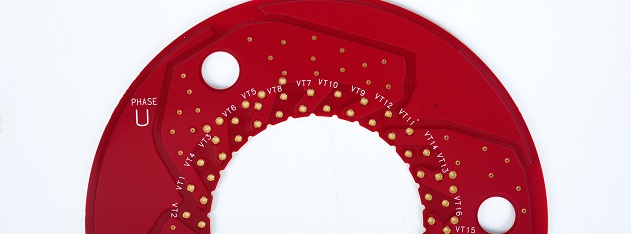
  • Component Mounting: Secure through-hole parts (e.g., connectors, switches).
  • Vias: Connect layers in multi-layer boards (e.g., smartphones, IoT devices).
  • High-Speed Circuits: Maintain signal integrity in 5G/RF designs.
  • Power Delivery: Support high-current paths for motor drivers.
  • Flexible PCBs: Prevent pad cracking in bending zones.
  • Automotive/Aerospace: Withstand vibration and thermal stress.
  • Medical Devices: Ensure reliability in critical applications.
  • Thermal Management: Link to heat sinks via thermal vias.
Annular Ring PCB

Design Considerations for Annular Ring

When designing PCBs, it’s essential to consider the following factors related to annular rings:

  • Width: Maintain ≄0.15mm (6 mils) for reliability; increase for high-stress areas.
  • Drill Size: Balance hole size with pad space; avoid oversizing to prevent weakness.
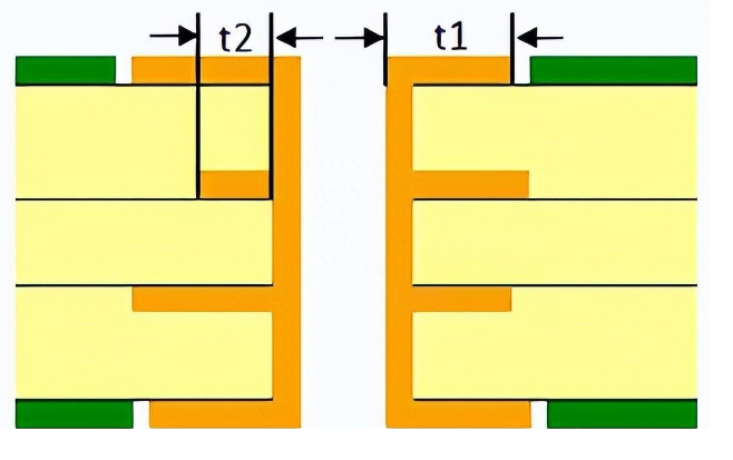
  • Layer Alignment: Ensure precise registration (±0.075mm tolerance) for multilayer boards.
  • Material Thickness: Thicker boards require wider rings (≄0.2mm) for connectivity.
  • Thermal/Mechanical Stress: Use tear-drop pads or wider rings (≄0.25mm) for durability.
  • Signal Integrity: Keep widths consistent for high-speed circuits; avoid impedance variations.
  • Assembly Clearance: Leave ≄0.2mm between rings and adjacent components for soldering.
  • Cost vs. Quality: Adjust widths based on application (e.g., 0.1mm for economy designs).
  • Testing: Validate rings via cross-section analysis and electrical tests.

Common Issues with Annular Ring PCB

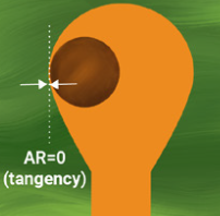
  • Breakout: Misaligned drilling causes holes to exceed pad boundaries, weakening connections.
  • Weak Connections: Insufficient width leads to poor solder joints or pad lift-off.
  • Signal Integrity Problems: Inconsistent widths create impedance discontinuities.
  • Thermal Stress Fractures: Narrow rings crack under repeated heating/cooling cycles.
  • Drill Deviation: Worn tools or poor registration enlarge holes, reducing annular ring margins.
  • Plating Voids: Uneven copper deposition in holes weakens annular ring conductivity.
  • Over-Etching: Excessive chemical etching undercuts pads, narrowing annular rings.
  • Mechanical Stress: Vibration or bending tears thin annular rings in rigid-flex designs.
  • Material Thickness Mismatch: Thick boards with small rings increase breakout risks.
  • Design Rule Violations: Ignoring IPC standards (e.g., minimum width) causes manufacturing failures.
Annular Ring PCB

How to Optimize Annular Ring in PCB Design

Below are ways to how to optimize annular ring in PCB design:

  • Adhere to Standards: Follow IPC-2221/IPC-6012 for minimum width (e.g., 0.05mm for Class 3 boards).
  • Design Software Tools: Use EDA tools (e.g., Altium, KiCad) for DRC checks and 3D visualization.
  • Material Selection: Choose for high-TG laminates to reduce thermal expansion affecting annular rings.
  • Thermal Management: Increase ring width or add thermal vias for heat-generating components.
  • Signal Integrity: Maintain consistent impedance by controlling trace-to-ring spacing.
  • Cost-Quality Balance: Widen rings for critical circuits; use narrower rings for non-critical areas.
  • DFM Checks: Validate designs for drill registration, copper weight, and aspect ratio.
  • Laser Drilling: For microvias, ensure annular rings ≄0.075mm to prevent breakout.
  • Tear-Drop Pads: Strengthen trace-to-pad junctions in high-flex or high-vibration applications.
  • Test Protocols: Use microsectioning and flying probe tests to verify annular ring quality.
  • Documentation: Clearly annotate ring requirements on fabrications drawings for manufacturers.

Why Choose Best Technology As a Annual Ring Manufacturer?

  • 18+ Years of Experience: With over 18 years in the PCB industry, we have the expertise to deliver high-quality annular ring PCBs tailored to your needs. 
  • Competitive Pricing: We offer the best quality products and services at the most competitive prices, ensuring value for your investment. 
  • No MOQ & Fully Flexible: Whether you need a prototype or medium-volume production, we accommodate orders of any size with no minimum order quantity. 
  • 99% On-Time Delivery: We prioritize timely delivery, ensuring your projects stay on schedule. 
  • ISO-Certified Quality: Our manufacturing processes adhere to ISO9001, ISO13485, and IATF16949 standards, guaranteeing reliable and consistent quality. 
  • Comprehensive Services: From PCB fabrication to assembly, component sourcing, and testing, we provide a one-stop solution for all your PCB needs. 
  • Industry-Specific Expertise: We understand the unique requirements of industries like medical, automotive, and aerospace, ensuring your PCBs meet the highest standards.  8. Customer-Centric Approach: Our goal is “Total Customer Satisfaction,” and we work closely with you to meet your specific requirements.

Contact Us Today

For high-quality PCBs with precise annular rings, trust Best Technology. Contact us today to discuss your project requirements and get a quote: sales@bestpcbs.com.

You may also like

Annular Ring: What is Annular Ring PCB? How to Calculate it?
Thursday, February 20th, 2025

Annular rings are small but essential features form part of the vias, helping to create electrical connections between different layers of the PCB. In simple terms, the annular ring is the copper ring that surrounds the hole in a PCB, and its quality can determine the effectiveness of the entire board. If not designed or manufactured correctly, the annular ring can lead to issues such as unreliable connections, potential failure, or even defective PCBs. In this blog, you’ll learn the importance in PCB design and functionality, how to calculate it correctly to avoid common issues occurred during PCB manufacturing.

What is Annular Ring in PCB?

To understand the importance of the annular ring, let’s break down its role in a PCB. A PCB is composed of multiple layers, and the annular rings on a PCB are circular metal rings used for mounting components on the circuit board. Sometimes, it also called PAD. They serve as connection points for the leads of electronic components and are attached to the corresponding positions on the board via soldering or insertion.

Annular Ring: What is Annular Ring PCB? How to Calculate it?

The annular rings are typically made of copper or other conductive materials, forming a connection around the holes to ensure that electrical signals can pass from one layer to another. Without this copper ring, the via would lack the necessary conductive material to transmit electrical signals, leading to potential functionality and reliability issues.

PCB holes usually come in shapes such as circular, square, or oblong. Among these, the circular hole is the most common. These holes are used for mounting components, connecting wires between circuit layers, or linking pads across different layers. When designing a PCB, you can select the appropriate hole shape based on specific needs.

What is an Annular Ring in Physics?

While the concept of the annular ring in PCB manufacturing is straightforward, it’s also rooted in basic physics. In physics, an annular ring is a two-dimensional geometric shape characterized by an outer and inner radius, with the space between the two radii representing the actual “ring.” This geometric shape has applications in a variety of fields, from fluid dynamics to optics.

In the context of PCB design, the annular ring’s geometry ensures that there’s enough copper material around the hole to support electrical connections and mechanical integrity. Essentially, the annular ring in PCB design mirrors this physical concept, providing the necessary structure to allow electrical signals to flow reliably between layers.

What is the Function of an Annular Ring?

The primary function of an annular ring is circuit connection. The annular ring connects with other circuit layers or components via wires or pins, enabling the transmission and interaction of electrical signals. Without this ring, the via would not have any conductive material to establish the necessary connections, rendering it ineffective. Essentially, the annular ring is like a bridge that connects different parts of the PCB. In addition to this, there are some other functions that apply annular rings in a PCB:

Annular Ring: What is Annular Ring PCB? How to Calculate it?

1. Component Mounting

    The annular ring is used to secure and connect electronic components (such as integrated circuit chips (IC), diodes, resistors, etc.) to the PCB through their leads or solder balls.

    2. Soldering Connection

    The metal edge of the annular ring is used for soldering the leads or pads of electronic components, establishing a reliable electrical connection. Through soldering, a physical and electrical bond is created between the component and the PCB.

    3. Vias in Multi-Layer PCBs

    In multi-layer PCBs, the annular ring serves as a via, acting as a conductive channel that connects different circuit layers. Through these vias, signals, power, and ground lines can be transmitted between layers.

    What is the Difference Between Via and Annular Ring?

    While vias and annular rings often work in tandem, they are different components of a PCB.

    Via:

    • A via is a drilled hole in the PCB, gennerally <=0.5mm.
    • It is plated with copper to create an electrical pathway.
    • Vias provide vertical connectivity between PCB layers.
    • They act as the conduits for electrical signals across layers.

    Annular Ring:

    • An annular ring is the copper pad that surrounds the via.
    • It creates a stable landing zone for the via.
    • The annular ring enhances solderability and connection strength.
    • It also supports the mechanical integrity of the PCB.

    Key Differences:

    • A via is the actual hole that allows electrical passage; the annular ring is the copper area around that hole.
    • Vias serve as internal conductive channels, while annular rings ensure a robust link to the board’s traces.
    • Vias are created by drilling and plating; annular rings are defined during the PCB layout design.

    In essence, the via acts as a hole or passage for electrical signals, while the annular ring is the surrounding copper that ensures the electrical signals can flow reliably between the different layers of the PCB. Without the annular ring, the via would have no copper to connect it to the surrounding traces, compromising the integrity of the circuit board.

    How Do You Calculate the Annular Ring Size?

    The annular ring size is determined by the diameter of the via hole and the size of the copper pad around it. To calculate the annular ring size, you need to first measure the diameter of the via hole. Then, you need to determine the size of the copper pad around the hole, keeping in mind that the pad must be large enough to maintain a reliable connection. In general, there are outer annular ring size and inner annular ring size:

    Outer Annular Ring Size (OAR)

    • Calculate Format:

    Outer Annular Ring (OAR) = (Outer pad diameter – Plated hole diameter) / 2

    • Actual Case:

    Plated hole diameter = Finished hole diameter + 0.10mm (for all PTH) + 0.00mm (for all NPTH).

    • Example:

    For a copper pad thickness of 0.60mm and a finished hole diameter of 0.30mm (PTH), the calculation of the OAR is:

    OAR = [0.60mm – (0.30mm + 0.10mm)] / 2 = 0.10mm

    Annular Ring: What is Annular Ring PCB? How to Calculate it?

    Inner Annular Ring Size (IAR)

    • Calculate Format:

    Inner Annular Ring (IAR) = (Inner pad diameter – Electroplated hole diameter) / 2

    • Actual Case:

    Electroplated hole diameter = Finished hole diameter + 0.10mm (for all PTH) + 0.00mm (for all NPTH).

    • Example:

    For a 0.50mm copper pad and a 0.20mm finished hole diameter (PTH), the calculation of the IAR is:

    IAR = [0.50mm – (0.20mm + 0.10mm)] / 2 = 0.10mm

    Annular Ring: What is Annular Ring PCB? How to Calculate it?

    What is the Minimum Annular Ring Size on a PCB?

    The minimum annular ring (AR) on a PCB refers to the minimum amount of copper between the edge of the pad and the electroplated hole. The width of the minimum annular ring should be greater than or equal to the value defined in the PCB design.

    Annular Ring: What is Annular Ring PCB? How to Calculate it?

    When the annular ring is smaller than the specified width, the attachment of components may be affected, and there is a risk of pad cracking. In this case, the circuit may enter the pad, minimizing the current-carrying capacity of the circuit.

    Sometimes, the traces on the PCB need to connect to another layer. In such cases, the trace eventually passes through the pad. The via in the pad helps the trace move through and connect to another layer.

    Annular Ring: What is Annular Ring PCB? How to Calculate it?
    • t1: Minimum outer annular ring, on finished boards, must be >= 0.05mm.
    • t2: Minimum inner annular ring, on finished boards, must be >= 0.01mm.

    Common Annular Ring Issues During PCB Manufacturing

    Despite the importance of annular rings, issues can arise during the manufacturing process that impact their effectiveness. Some common problems include:

    • Undesired Annular Rings

    Undesired annular rings are a common issue that affects many designers when working with standard PCBs. If the pad size is too small, the PCB may not function properly because the hole takes up more space on the pad. To avoid this issue, making a prototype before mass production is necessary. Prototypes can prevent unnecessary annular rings from appearing before large-scale production of the circuit boards.

    • Missing Annular Ring

    A missing annular ring can occur if the design does not include an annular ring around the via, or if the annular ring was not correctly produced during manufacturing. This can lead to poor electrical connections, affecting the performance of the circuit.

    • Broken Annular Ring

    A broken annular ring occurs when drill tolerances cause the via to deviate from the center during manufacturing, leading to the annular ring breakout.

    Annular Ring: What is Annular Ring PCB? How to Calculate it?
    • Annular Ring Tangency

    Annular ring tangency refers to a situation where part of the via touches the edge of the pad, typically caused by the drill bit not being aligned with the markings. This can cause the via to deviate from the center and negatively affect the normal operation of the circuit.

    Annular Ring: What is Annular Ring PCB? How to Calculate it?

    What Can Best Technology Do for You?

    At Best Technology, we have over 18 years of experience in PCB manufacturing, and we understand the importance of the annular ring in creating reliable and high-quality PCBs. Our team of experts works closely with clients to ensure that every PCB is designed with the right annular ring specifications, minimizing the risk of defects and improving the overall performance of the circuit board. In additional to this, our sales-assistant will send EQ (engineer question) file and WF (working file for manufacturing) to customer for a final approval before starting production.

    We use state-of-the-art equipment and precision techniques to manufacture PCBs that meet the highest standards. Whether you’re designing a single-layer PCB or a complex multi-layer board, Best Technology has the expertise and experience to deliver high-quality PCBs that meet your needs. We’re here to support your projects and ensure that your PCBs are reliable, efficient, and built to last.

    Let us help you create the perfect PCB with the right annular ring design to ensure seamless electrical connections and superior functionality. Reach out to Best Technology today for your PCB needs!

    You may also like