

What is aluminum metal core PCB? Let’s explore its definition, pros and cons, applications, technical parameter, design guide and production processes through this blog.
Are you worried about these problems?
- Always rejected for small orders? How to avoid R&D delays?
- LED heat dissipation issues causing fast light decay? How to extend lifespan?
- High costs from fragmented component sourcing? How to protect profit margins?
As an aluminum PCB manufacturer, EBest Circuit (Best Technology) can provide you service and solutions:
- Flexible Quick Response – Start from 1 piece, 48-hour rapid prototyping. Small orders get fast design validation without compromise.
- Direct Sourcing Cost Reduction – Direct links to TI/NXP and certified distributors. Centralized negotiation and shared inventory slash BOM costs by 15-25%.
- Digital Process Control – DFM automatic verification + real-time progress dashboard. Production cycle cut by 30%, full traceability from cutting to assembly.
Welcome to contact us if you have any inquiry for aluminum metal core PCB: sales@bestpcbs.com.
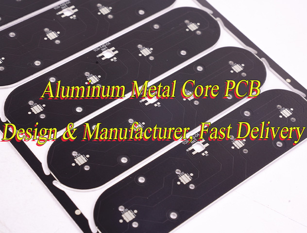
What Is Aluminum Metal Core PCB?
Aluminum Metal Core PCB is an aluminum-based printed circuit board designed for efficient thermal management. It achieves this through a sandwich structure consisting of an aluminum substrate, insulating layer, and copper circuit layer. The aluminum substrate rapidly dissipates heat generated by electronic components, preventing thermal buildup. This makes it ideal for high-power applications including LED lighting, automotive electronics, and power modules. The design combines lightweight construction, cost efficiency, and high reliability, making it a preferred solution for thermal-sensitive electronic systems.
What Are the Pros and Cons of Aluminum PCB?
Pros of aluminum metal core PCB
- Efficient Thermal Management: Thermal conductivity of 1-9 W/m·K, significantly higher than FR4 (0.3-0.4 W/m·K). Rapidly dissipates heat from high-power components like LEDs and power modules, preventing thermal failure.
- Lightweight Design: Aluminum density of 2.7 g/cm³, 65% lighter than copper. Ideal for weight-sensitive applications such as automotive electronics and consumer devices.
- Cost Efficiency: Material costs 30-50% lower than copper. Reduces overall system costs through bulk procurement and minimized need for external heat sinks.
- High Mechanical Strength: Resistant to vibration and impact, extending device lifespan. Suitable for harsh environments like industrial and automotive sectors.
- Environmentally Friendly & Recyclable: 100% recyclable aluminum. Production aligns with RoHS standards and green manufacturing trends.
- Wide Temperature Adaptability: Operates reliably from -40°C to 150°C. Optimized thermal expansion matching reduces warpage risks.
Cons of aluminum metal core PCB
- Thermal Conductivity Limit: Aluminum’s 237 W/m·K thermal conductivity is lower than copper’s 400 W/m·K. Requires careful evaluation for ultra-high-power scenarios.
- CTE Mismatch Challenges: Significant thermal expansion coefficient differences between aluminum, copper, and insulating layers can cause interlayer stress, warpage, or solder joint failures. Demands structural/material optimization.
- Complex Manufacturing Process: Requires specialized equipment (e.g., laser drilling, anodizing). Higher initial costs and strict yield control requirements.
- Limited Flexibility: High hardness and low toughness make it unsuitable for flexible circuits or designs requiring bending.
- Humidity Sensitivity: Prone to moisture-related issues. Requires sealing/anti-humidity coatings to prevent insulation failure.
- Electrical Performance Constraints: Lower conductivity than copper. High-frequency or precision circuits need additional design compensation.
- Processing Defect Risks: Potential burrs/copper residues from etching/drilling. Requires precision process control (e.g., ±0.1mm line width tolerance).
- Cost-Volume Trade-off: Thick aluminum substrates (e.g., 3mm) may increase bulk. Budget-conscious projects must balance cost-benefit ratios.
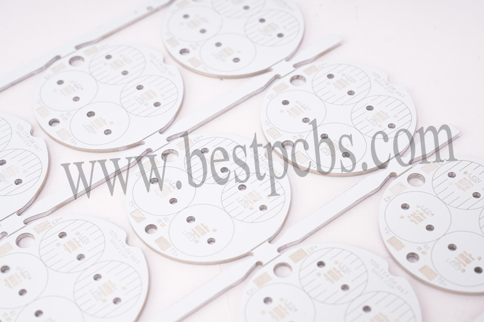
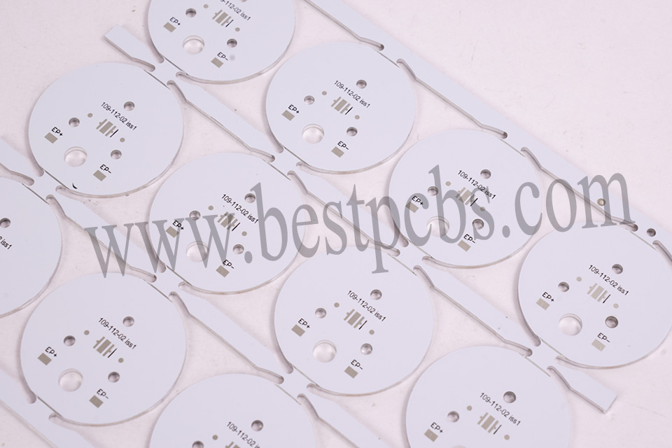
What Are Applications of Aluminum Metal Core PCB?
Applications of aluminum metal core PCBs:
- LED Lighting: Street lamps, stage lights, display backlight modules.
- Automotive Electronics: LED headlights, battery management systems (BMS), motor controllers.
- Power Modules: Switching power supplies, inverters, power amplifiers.
- Industrial Automation: PLC controllers, motor drivers, sensor modules.
- Medical Devices: Medical imaging systems, laser therapy devices, vital sign monitors.
- Consumer Electronics: Gaming consoles, premium audio amplifiers, TV driver boards.
- Aerospace & Defense: Satellite power modules, radar cooling components, spacecraft thermal control systems.
Aluminum Metal Core PCB Design Technical Parameter
| Parameter Name | Technical Parameter |
| Layer Count | 1-2 layers (single/double-sided) |
| Board Thickness | 0.5-3.0mm |
| Copper Thickness | 1-10oz (35-350µm) |
| Thermal Conductivity (Aluminum Base) | 1.0-4.0W/m·K (standard); 180-240W/m·K (high-conductivity version) |
| Thermal Resistance | 1.0-2.5°C/W (full board); 0.05-0.2K/W (localized) |
| Operating Temperature | -40°C~150°C (standard); peak 260°C |
| Aluminum Material Type | 3003/5052/6061 alloy |
| Insulation Layer Material | Epoxy resin (0.2-0.3W/m·K); ceramic-filled (1-5W/m·K); aluminum nitride (150-180W/m·K) |
| Insulation Strength | ≥3000V (standard); 1500-6000V (high-voltage) |
| Minimum Trace Width/Spacing | 0.1mm (outer layer); 0.13mm (inner layer) |
| Drill Hole Diameter | 0.7-1.0mm (matched to board thickness) |
| Surface Finish | HASL/lead-free HAL/ENIG/OSP |
| Peel Strength | ≥1.0N/mm |
| CTE Matching | Aluminum (23-24ppm/°C); copper (17ppm/°C) |
| Environmental Standards | RoHS compliant |
| Maximum Panel Size | 600×500mm |
How to Design LED Aluminum Metal Core PCB?
Below is LED aluminum metal core PCB design guide:
1. Material & Substrate Selection
- Use aluminum alloys (5052/6061) with thermal conductivity 1.0–9.0 W/m·K and thickness 0.8–3.2mm.
- Pair with 1–2 oz copper foil and polyimide/epoxy dielectric layers (≥0.1mm thickness) for electrical isolation.
- For low-power (<5W) systems, FR4 with thermal vias (≥0.5mm diameter) can be substituted; avoid laminates with <0.3 W/m·K conductivity. Specify no-flow prepreg for direct LED-to-metal bonding to reduce thermal resistance.
2. Layer Stackup & Thermal-Electrical Co-Design
- Configure layer stacks: single-layer for <2A, double-layer for 2–5A, or 4+ layers for complex systems. Use 2+ oz copper for power/ground planes; maintain ≥0.5mm trace width for >5A currents.
- Place thermal vias (≥1.0mm diameter) in 3×3 grids under LEDs to achieve thermal resistance <4×10⁻⁴ °C/W. Dedicate layers for 50Ω impedance-controlled high-speed signal paths (e.g., PWM dimming).
3. Thermal Management Implementation
- Integrate thermal vias, heat sinks, and TIMs (5.0–10.0 W/m·K graphite pads) to optimize heat dissipation. Design heat sinks with fin spacing ≥5mm for natural convection or use forced-air cooling channels.
- Simulate thermal paths using ANSYS Icepak or FLOTHERM; target junction temperature <125°C and ΔT ≤30°C between LED junction and case. Use IR thermal cameras to validate hotspot mapping and thermal efficiency.
4. Component Placement & Light Uniformity
- Arrange LEDs in symmetric grids/linear rows with 1.5–3.0mm spacing for uniform light distribution.
- Place high-current components (drivers, MOSFETs) near copper planes to minimize loop inductance. Avoid placing SMD components within 2mm of thermal vias to prevent solder joint fatigue.
- Use 3D CAD tools to verify shadow-free placement and beam angle alignment (e.g., 120° for uniform illumination).
5. Electrical Layout & Power Integrity
- Widen power traces to ≥0.5mm for >5A currents; implement Kelvin connections for current-sense resistors (<10mΩ).
- Design differential pairs with 100±10Ω impedance for PWM dimming signals to reduce EMI.
- Include ESD protection diodes (e.g., TVS) at I/O ports and use ground planes to mitigate noise.
- Place low-ESL capacitors (e.g., X7R) near LEDs for decoupling; limit current-sense resistor values to <10mΩ.
6. Manufacturing & Assembly Process
- Specify ENIG or OSP surface finishes for corrosion resistance and solderability.
- Use solder paste stencils with 0.12mm aperture for fine-pitch LEDs; implement panelization with 5–10mm breakaway tabs.
- Perform in-circuit testing (ICT) for opens/shorts and automated optical inspection (AOI) for solder joint quality.
- Validate with thermal cycling (-40°C to +125°C, 1000 cycles) and vibration testing per IPC-TM-650 standards.
7. Reliability Testing & Standards Compliance
- Conduct LTOL (1000h at 85°C/85% RH), HTOL (1000h at 125°C), and thermal shock (-55°C to 125°C, 500 cycles).
- Measure voltage drops using 4-wire Kelvin probes; verify ΔT ≤30°C via IR thermal imaging.
- Ensure compliance with UL 8750 for LED lighting safety, IEC 61000-4 for EMC immunity, and JEDEC standards for reliability.
- Document test results in formal reports including thermal, electrical, and mechanical validation data.
LED Aluminum Metal Core PCB Production Processes
1. Material Cutting and Substrate Preparation
- Substrate Selection: High-thermal-conductivity aluminum alloy (e.g., 5052/6061 series), thickness 0.4-3.2mm, certified to ISO 9001. Stress relief through 150℃/4-hour baking, surface roughness Ra≤1.6μm, dimensional tolerance ±0.1mm.
- Pretreatment: Ultrasonic + chemical cleaning (acidic/alkaline agents) to remove grease and oxides. Surface treatments include chemical oxidation (0.1-0.3μm) or anodizing (5-20μm) to enhance adhesion between aluminum and insulation layers. Edge grinding via CNC milling with chamfer R0.5-1mm to prevent interlayer short circuits.
2. Insulation Layer Deposition and Copper Foil Lamination
- Insulation Coating: High-thermal-conductivity epoxy resin/ceramic filler (1-3W/mK thermal conductivity) applied via screen printing or inkjet, thickness 6-12mil (±10%). Curing at 150℃/60 minutes to match aluminum’s CTE (22-24ppm/℃).
- Copper Foil Lamination: Vacuum hot press (180-220℃, 2-3MPa), copper foil thickness 1-6OZ (18-210μm), interlayer bonding strength ≥1.4N/mm (per IPC-TM-650). Temperature curve monitoring to avoid blistering or delamination.
3. Pattern Transfer and Etching
- Photoresist Application: Dry film (1.3-2.5mil thickness) exposure at 300-500mJ/cm², development with 0.8-1.2% Na₂CO₃ solution at 30±2℃, ±10-second development time tolerance.
- Precision Etching Control: Vertical continuous etching line, etching factor ≥3:1. For 1OZ copper, etching time 2-3 minutes, solution copper ion concentration 140-160g/L, undercut ≤10% of line width. Post-etch line spacing ≥0.02mm design value, AOI defect density ≤0.1mm²/m².
4. Drilling and Metallization
- Drilling Process: High-precision drilling machine (20,000-60,000 RPM, 1-1.5mil/rev feed), drill bit diameter 0.1-3mm, hole wall roughness Ra≤3.5μm. Post-drilling deburring (mechanical polishing/plasma cleaning), hole position tolerance ±0.05mm (standard holes) or ±0.03mm (blind/buried holes).
- Hole Metallization: Chemical copper plating (0.5-1μm) + electroplating (20-25μm), plating uniformity ≥85%, hole copper thickness tolerance ±3μm. Backlight test (≥9-grade) and thermal shock test (288℃/10s ×3 cycles, no delamination).
5. Solder Mask and Surface Treatment
- Solder Mask Application: Photosensitive solder mask ink (15-25μm thickness), pre-bake at 80℃/30 minutes, exposure energy 20% higher than circuit layer, post-development solder mask bridge width ≥0.1mm. Curing at 150℃/40 minutes, hardness ≥2H (pencil hardness).
- Surface Treatments: ENIG (gold 0.05-0.15μm, nickel 3-5μm), OSP (0.2-0.5μm), or HASL (SnPb 5-8μm). ENIG passes porosity test (≤10 defects/cm²), OSP solderable within 24 hours.
6. Profiling and Inspection
- Profile Machining: CNC milling (±0.1mm accuracy) or laser cutting (±0.05mm accuracy), edge burr height ≤5μm. V-cut depth at 1/3 of board thickness to prevent edge cracking.
- Quality Inspection: AOI for circuit defects (shorts/opens), X-ray for hole alignment (error ≤0.05mm), thermal cycling (-40℃~125℃/500 cycles, no delamination), impedance test error ≤±10%. Final FQC/FQA sampling per IPC-A-600.
7. Assembly and Testing
- Component Soldering: SMT placement via high-precision pick-and-place machine (±0.05mm accuracy), soldering profile (preheat 150℃/60s, peak 235℃/3s). LED chips require ESD protection (HBM ≥2000V), solder joint pull strength ≥5N (per JESD22-B116).
- Functional Testing: Electrical performance (voltage/current/power), burn-in test (85℃/85% RH/1000 hours), optical performance (lumen/color temperature/CRI). Pre-packaging vacuum sealing (humidity ≤5%), transport temperature 15-30℃ to avoid vibration damage.
How to Balance Performance and Cost of LED Aluminum PCB?
Material Selection and Cost Balance
- Prioritize 5052 aluminum alloy (high cost-performance) over 6061, with thickness controlled at 1.0–2.0mm to balance thermal dissipation and material costs.
- For low-power scenarios (<3W), use FR4 substrate with ≥0.5mm thermal vias. Compare polyimide (high thermal conductivity, higher cost) and epoxy resin (low-cost) insulation layers: select polyimide for high heat dissipation needs and epoxy for general applications.
Layer Design and Signal Optimization
- Single-layer PCBs suit simple applications like 12V LED strips, reducing costs by 30–40% compared to multilayer designs. Use double-layer boards for >2A currents or complex routing; avoid >4 layers unless high-speed signals (e.g., PWM dimming) require impedance control.
- Combine power and ground planes in a single copper layer with 2oz thick copper to reduce layer count while maintaining current capacity.
Thermal Solution Cost Optimization
- In low-cost scenarios, replace expensive graphite sheets with silicone pads (thermal conductivity: 1.5–3.0 W/m·K). Use 2×2 thermal via arrays (≥0.8mm diameter) instead of 3×3 arrays to cut drilling costs.
- For high-power LEDs (>5W), adopt aluminum extrusion heat sinks (low cost) with optimized fin spacing of 3–5mm for natural convection, minimizing material waste.
Component Selection and Standardization
- Optimize for economical packages like 2835 SMD LEDs ($0.01–$0.03/unit) instead of high-brightness COB modules ($0.10+/unit). Choose common capacitors/resistors for procurement ease.
- Standardize to 0805/1206 footprints for compatibility with automated SMT lines, reducing assembly costs by 15–25%.
Manufacturing Process Cost Control
- Use OSP surface finish ($0.05–$0.10/sq in) for non-corrosive environments instead of costly ENIG. Reserve ENIG for critical pads in high-reliability needs.
- Optimize stencil design: laser-cut stencils ($100–$200/board) for mass production, etched stencils ($20–$50) for small batches. Reduce solder paste usage by shrinking stencil apertures.
Testing and Validation Cost Reduction
- Replace full thermal cycling tests with HALT sampling (3–5 units), cutting inspection costs by 50–70%. Use rapid thermal imagers instead of full-board thermal imaging.
- Deploy AOI systems for in-house solder joint checks, reducing outsourced testing expenses. Utilize open-source EDA tools for DRC checks, eliminating commercial software licensing fees.
Scalability and Long-Term Cost Management
- Design modular architectures (e.g., separate driver and LED modules) for phased upgrades over full redesigns. Adopt standardized connectors (e.g., XH series) to lower wiring costs and simplify maintenance.
- Negotiate volume discounts (10–20% for orders >500 units) with manufacturers. Improve material utilization via panelization (e.g., 10 units per board) to reduce per-unit costs.
Why Choose EBest Circuit (Best Technology) as Aluminum Metal Core PCB Manufacturer?
Reasons why choose us as aluminum metal core PCB manufacturer:
- 19 Years of Aluminum Metal Core PCB Production Expertise: Leverage 19 years of industry-specific experience to ensure mature manufacturing processes and stable production capacity, reducing technical risks by 30% and guaranteeing first-pass project success.
- 24-Hour Rapid Prototyping & Shipping for Urgent Orders: Accelerate product development cycles by 40% through 24-hour turnaround for prototyping and shipping, enabling clients to seize market opportunities ahead of competitors.
- Multi-Layer Strict Quality Control System: Implement full-process quality management from raw material inspection to final testing, maintaining defect rates below 0.3% to minimize post-sales maintenance costs and ensure product reliability.
- Transparent Pricing with No Hidden Costs: Adopt an open pricing model detailing all cost components (materials, processes, testing) to eliminate unexpected fees, ensuring precise budget control for clients.
- Dual-Tier Certifications (Automotive & Medical Grade): Hold IATF 16949 (automotive) and ISO 13485 (medical) certifications to meet stringent industry standards, enhancing market access and compliance credibility for specialized applications.
- Full Turnkey Solutions: Streamline project execution by covering design support, prototyping, volume production, and logistics under one roof, reducing coordination efforts with multiple vendors and improving efficiency by 25%.
- Free DFM (Design for Manufacturability) Support: Utilize expert engineering teams to provide complimentary DFM analysis, optimizing PCB layout and thermal management to reduce R&D iterations and associated costs.
- Customizable Material & Process Selection: Offer flexible substrate options (e.g., 5052/6061 aluminum, FR4 hybrid) tailored to performance-cost requirements, maximizing product value through strategic material choices.
- Eco-Friendly Production & Compliance Assurance: Employ lead-free processes and RoHS-compliant materials, supported by environmental test reports, to facilitate global market compliance and environmental sustainability goals.
- Global Logistics & 24/7 Rapid Response Support: Ensure 72-hour global delivery via an optimized logistics network and localized warehousing, complemented by 24-hour customer service to address urgent needs promptly.
Welcome to contact us if you have any request for aluminum metal core PCB: sales@bestpcbs.com.