

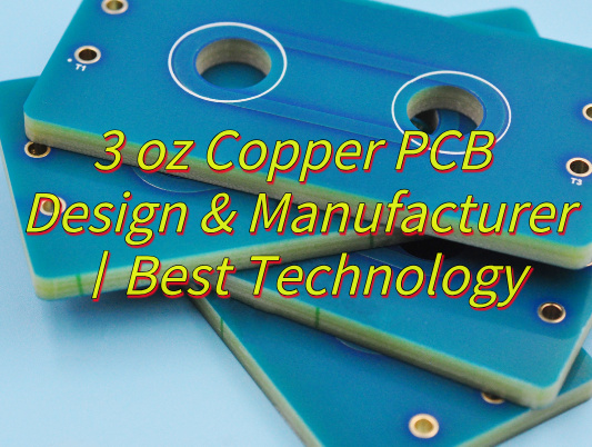
What is 3 oz copper PCB? Let’s explore thickness, current capability, advantages, applications, design guide and how to get a quote for 3 oz copper PCB.
Are you troubled with these issues?
- PCB temperature rises uncontrollably under high current conditions. How can I overcome the heat dissipation bottleneck?
- What should I do if impedance fluctuations increase bit error rates during high-frequency signal transmission?
- The copper thickness compliance rate for multilayer boards is low after lamination. How can I ensure consistent quality?
EBest Circuit (Best Technology) can provide solution:
- Micro-etching + electroplating fill process: Using proprietary surface treatment technology, we achieve a 3oz copper thickness tolerance of ±8μm, improving heat dissipation efficiency by 40%.
- Impedance simulation and compensation design: Provide pre-DFM analysis services to proactively compensate for the impact of copper thickness on impedance, ensuring signal loss <3dB
- Vacuum lamination intelligent temperature control system: Using a segmented pressurization process to eliminate delamination issues in heavy copper clad plates, maintaining a stable yield rate above 98.5%.
Welcome to contact us if you have any request for 3 oz copper PCB: sales@bestpcbs.com.
What Is 3 oz Copper PCB?
A 3 oz copper PCB is a type of heavy copper PCB that features a copper thickness of 3 ounces per square foot, significantly thicker than standard 1 oz (35 µm) PCBs. This design is ideal for high-power applications, such as power supplies, automotive electronics, and industrial equipment, where it can handle higher current loads, dissipate heat more effectively, and enhance mechanical durability. The increased copper thickness also reduces resistance and improves thermal management, making it a reliable choice for demanding environments.
How Thick is 3 oz of Copper on a PCB?
3 oz of copper on a PCB measures approximately 105 micrometers (µm) in thickness, equivalent to 4.13 mils, which is three times thicker than standard 1 oz (35µm) copper foil. This thickness is calculated based on the weight of copper per square foot, where 1 oz equals 28.35 grams spread over 1 square foot (0.0929 m²), with 3 oz representing three times that mass density.
What Is the Current of 3 oz Copper PCB?
A 3 oz (105µm) copper PCB can typically handle 22–30A per 1mm width at a 20°C temperature rise, depending on whether the trace is on the inner or outer layer (inner layer: ~22A/mm; outer layer: ~30A/mm). This capacity is derived from IPC-2221 standards, which consider copper thickness, trace width, and allowable temperature rise. For example, a 10mm-wide trace on an outer layer could theoretically carry 300A with proper thermal management.
Why Choose 3 oz Copper PCB?
- Higher Current Capacity – Supports up to 30A/mm on outer layers, enabling stable operation for high-power applications without excessive heating.
- Improved Thermal Management – Thicker copper dissipates heat more efficiently, reducing thermal stress and prolonging component lifespan.
- Enhanced Durability – Resists mechanical stress and thermal cycling better than thinner copper, ideal for demanding environments.
- Space Efficiency – Allows for wider traces or fewer layers in high-current designs, simplifying PCB layouts and reducing costs.
- Reliable Performance – Minimizes voltage drop and signal loss, ensuring consistent power delivery in industrial and automotive applications.
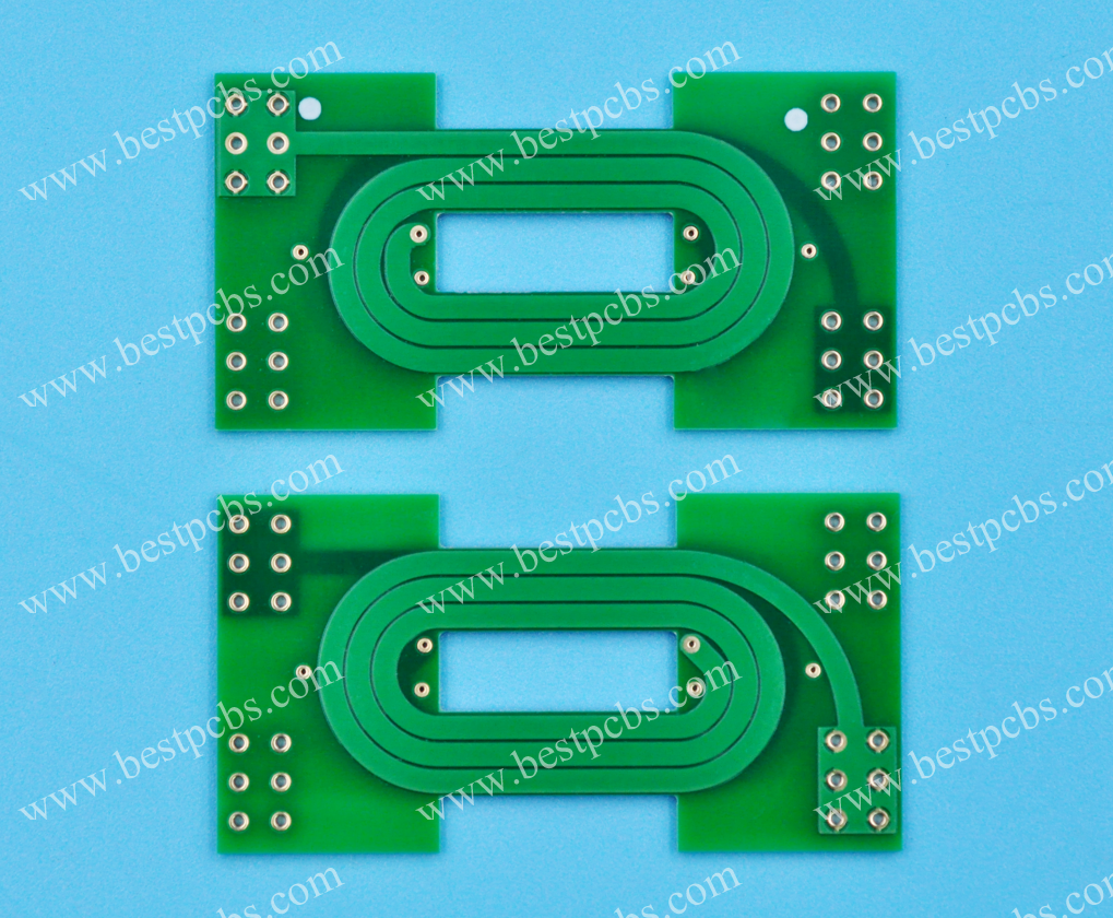
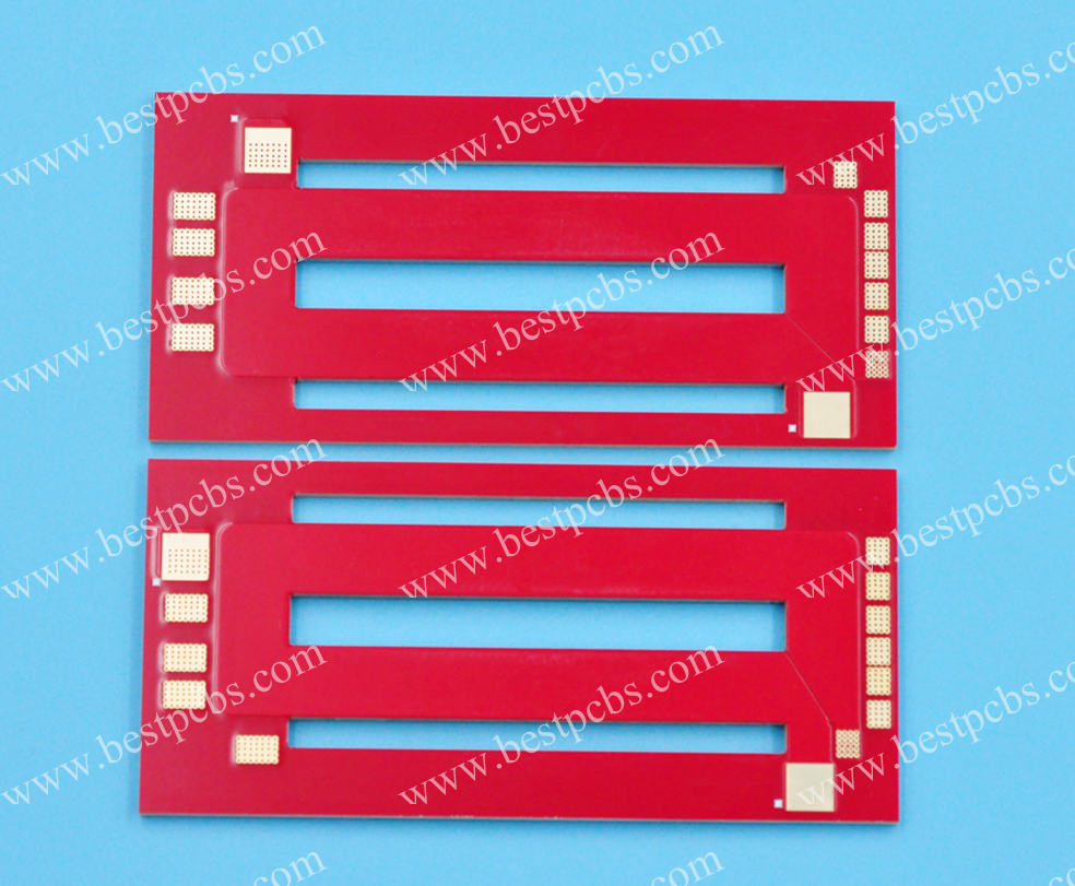
When to Use 3oz Copper PCB?
- High-Current Power Applications: Power supplies, motor controllers, battery management systems (BMS), and solar inverters require thick copper (3oz) to minimize resistive losses and heat generation under heavy loads.
- Thermal Management-Critical Systems: Automotive engine control units (ECUs), industrial power converters, and LED drivers use 3oz copper to enhance heat dissipation, reducing reliance on external heatsinks.
- RF/Microwave Power Amplifiers: Thick copper layers improve current handling in high-frequency power circuits, minimizing signal loss and thermal stress in wireless communication/radar systems.
- Mechanically Demanding Environments: Aerospace, military, and automotive PCBs subject to vibration, shock, or thermal cycling use 3oz copper for structural durability and reduced risk of trace fatigue.
- Corrosion-Resistant/Outdoor Electronics: Marine, industrial automation, and outdoor IoT devices benefit from thicker copper’s resistance to humidity, salt, and chemical exposure, ensuring long-term reliability.
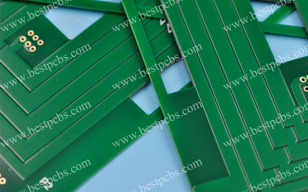
3 oz Copper PCB Design Guide
Below are 3 oz copper PCB design guide:
1. Requirement Analysis
- Define current capacity, thermal limits, and mechanical stress tolerance.
- Confirm PCB layer stackup (e.g., 4-layer: signal-GND-power-signal).
2. Layer Stackup Design
- Assign 3 oz copper to power/ground planes and high-current signal layers.
- Use 0.2mm FR4 dielectric between layers for thermal and electrical performance.
3. Layout Planning
- Place power components (e.g., MOSFETs, inductors) close to power planes.
- Isolate high-current traces from sensitive signals to avoid EMI.
4. Trace Width Calculation
- Use IPC-2221 or online calculators to determine trace width based on max current and 3 oz copper thickness.
- Example: 10°C temp rise → 10mil trace = 6A (vs. 2A for 1 oz).
5. Thermal Management
- Add thermal vias under high-power components to connect top/bottom layers.
- Use solid copper pours for power/ground planes to minimize resistance.
6. Impedance Control (If Needed)
- For high-speed signals, adjust trace geometry (width/spacing) to account for 3 oz copper’s thicker profile.
7. Manufacturability Check
- Confirm PCB fab capabilities for 3 oz copper (minimum trace/space, plating uniformity).
- Avoid sharp angles in high-current traces to prevent etching issues.
Reliable 3 oz Copper PCB Manufacturer – EBest Circuit (Best Technology)
Reasons why choose us as 3 oz copper PCB manufacturer:
- Global Certifications – Compliant with IPC, UL, and RoHS standards for reliable global shipments.
- Ultra-Fast Delivery – Emergency orders processed in 24 hours to meet urgent project timelines.
- Strict Quality Control – Full inspection for bulk orders, ensuring defect rates below 0.1%.
- 19 Years of heavy copper PCB Manufacturing Expertise – Proven ability to troubleshoot complex production issues efficiently.
- Cost-Effective Pricing – Transparent pricing with no hidden fees, offering 15-20% cost savings vs. competitors.
- Free DFM Analysis – Pre-production checks reduce rework costs by up to 30%.
- First-Pass Prototype Success – 98% first-time sample approval rate, minimizing iteration expenses.
- 24/7 Engineer Support – Real-time technical assistance to resolve design or production concerns.
- Flexible MOQ – Supports low-volume prototypes (1-10pcs) to mass production (10,000+ pcs).
Our Heavy Copper PCB Capabilities
| Base material | FR4/Aluminum |
| Copper thickness | 4 OZ~10 OZ |
| Extreme Heavy Copper | 20~200 OZ |
| Outline | Routing, punching, V-Cut |
| Soldermask | White/Black/Blue/Green/Red Oil |
| Surface finishing | Immersion Gold, HASL, OSP |
| Max Panel size | 580*480mm(22.8″*18.9″) |
How to Get a Quote for Your Heavy Copper PCB Project?
Required Information for an Accurate Quote
- PCB Specifications – Layer count, dimensions, thickness (e.g., 2.0mm), and copper weight (e.g., 3 oz).
- Material Requirements – Base material (FR-4, Rogers, etc.), Tg value, and surface finish (ENIG, HASL, etc.).
- Gerber Files & Drill Data – Provide updated Gerber files (RS-274X format) and drill files (Excellon).
- Technical Drawings – Include impedance control, stackup design, and tolerance requirements.
- Special Processes – Specify if blind/buried vias, edge plating, or heavy copper balancing are needed.
- Testing Standards – Define electrical testing (e.g., flying probe) and reliability tests (thermal cycling).
- Quantity & Lead Time – Prototype/batch quantity and desired delivery timeline (e.g., 24-hour rush service).
- Certifications – Required certifications (UL, IPC Class 2/3, RoHS, etc.).
Why Choose EBest Circuit (Best Technology)?
- 19+ Years Expertise – Specialized in heavy copper PCBs (up to 20 oz) with high-current and thermal management solutions.
- One-Stop Service – From DFM analysis to assembly, ensuring design-to-delivery consistency.
- Transparent Pricing – No hidden fees; competitive rates with bulk-order discounts.
- Fast Turnkey – 24-hour prototyping and 15-day mass production.
Contact us for a quote now: sales@bestpcbs.com. Looking forward to hearing from you soon!